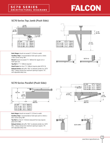
Transcription
19-1862; Rev 4; 1/07SC70, 1.6V, Nanopower, Beyond-the-RailsComparators With/Without ReferenceThe MAX9117–MAX9120 nanopower comparators inspace-saving SC70 packages feature Beyond-theRails inputs and are guaranteed to operate down to 1.6V. The MAX9117/MAX9118 feature an on-board1.252V 1.75% reference and draw an ultra-low supplycurrent of only 600nA, while the MAX9119/MAX9120(without reference) require just 350nA of supply current.These features make the MAX9117–MAX9120 family ofcomparators ideal for all 2-cell battery-monitoring/management applications.The unique design of the output stage limits supply-current surges while switching, virtually eliminating the supply glitches typical of many other comparators. Thisdesign also minimizes overall power consumption underdynamic conditions. The MAX9117/MAX9119 have apush-pull output stage that sinks and sources current.Large internal-output drivers allow rail-to-rail outputswing with loads up to 5mA. The MAX9118/MAX9120have an open-drain output stage that makes them suitable for mixed-voltage system design. All devices areavailable in the ultra-small 5-pin SC70 package.Features Space-Saving SC70 Package (Half the Size ofSOT23) Ultra-Low Supply Current350nA Per Comparator (MAX9119/MAX9120)600nA Per Comparator with Reference(MAX9117/MAX9118) Guaranteed to Operate Down to 1.6V Internal 1.252V 1.75% Reference(MAX9117/MAX9118) Input Voltage Range Extends 200mVBeyond-the-Rails CMOS Push-Pull Output with 5mA DriveCapability (MAX9117/MAX9119) Open-Drain Output Versions Available(MAX9118/MAX9120) Crowbar-Current-Free Switching Internal Hysteresis for Clean Switching No Phase Reversal for Overdriven InputsOrdering InformationApplicationsPINPACKAGEPART2-Cell Battery Monitoring/ManagementUltra-Low-Power SystemsMAX9117EXK-T5 SC70-5TOPMARKPKGCODEABWX5-1—S8-2Mobile CommunicationsMAX9117ESA 8 SONotebooks and PDAsMAX9118EXK-T5 SC70-5ABXX5-1MAX9119EXK-T5 SC70-5ABYX5-1MAX9120EXK-T5 SC70-5ABZX5-1MAX9120ESA 8 SO—S8-2Threshold Detectors/DiscriminatorsSensing at Ground or Supply LineTelemetry and Remote SystemsNote: All devices specified for over -40 C to 85 C operatingtemperature range. Denotes lead-free package.Medical InstrumentsSelector GuidePin YCURRENT(nA)TOP VIEWMAX9117YesPush-Pull600OUT 20NoOpen-Drain350VEE 25VCC8N.C.7VCCIN 36OUTVEE 45N.C.IN- (REF) 2MAX9117MAX9118MAX9119MAX9120IN 3N.C. 14IN- (REF)MAX9117MAX9120Typical Application Circuit appears at end of data sheet.Beyond-the-Rails is a trademark of Maxim Integrated Products, Inc.SC70SO( ) ARE FOR MAX9117/MAX9118.Maxim Integrated ProductsFor pricing, delivery, and ordering information, please contact Maxim/Dallas Direct! at1-888-629-4642, or visit Maxim’s website at www.maxim-ic.com.1MAX9117–MAX9120General Description
MAX9117–MAX9120SC70, 1.6V, Nanopower, Beyond-the-RailsComparators With/Without ReferenceABSOLUTE MAXIMUM RATINGSSupply Voltage (VCC to VEE). 6VVoltage Inputs (IN , IN-, REF) .(VEE - 0.3V) to (VCC 0.3V)Output VoltageMAX9117/MAX9119 .(VEE - 0.3V) to (VCC 0.3V)MAX9118/MAX9120 .(VEE - 0.3V) to 6VCurrent Into Input Pins. 20mAOutput Current. 50mAOutput Short-Circuit Duration .10sContinuous Power Dissipation (TA 70 C)5-Pin SC70 (derate 2.5mW/ C above 70 C) .200mW8-Pin SO (derate 5.88mW/ C above 70 C).471mWOperating Temperature Range .-40 C to 85 CJunction Temperature . 150 CStorage Temperature Range .-65 C to 150 CLead Temperature (soldering, 10s) . 300 CStresses beyond those listed under “Absolute Maximum Ratings” may cause permanent damage to the device. These are stress ratings only, and functionaloperation of the device at these or any other conditions beyond those indicated in the operational sections of the specifications is not implied. Exposure toabsolute maximum rating conditions for extended periods may affect device reliability.ELECTRICAL CHARACTERISTICS—MAX9117/MAX9118 (with REF)(VCC 5V, VEE 0V, VIN VREF, TA -40 C to 85 C, unless otherwise noted. Typical values are at TA 25 C.) (Note 1)PARAMETERSupply Voltage RangeSYMBOLVCCCONDITIONSInferred from the PSRR TA 25 CtestTA TMIN to TMAXVCC 1.6VSupply CurrentICCVCC 5V1.65.51.85.510.681.3TA TMIN to TMAXInput Offset VoltageVOS(Note 2)Input-Referred HysteresisVHB(Note 3)TA 25 CVEE 0.2VCC 0.214TA TMIN to TMAX0.1VCC - VOHVCC 5V, ISINK 5mAISINK 1mAISCSinking, VO VCCHigh-to-Low Propagation Delay(Note 4)2tPD-1190TA TMIN to TMAXVCC 1.6V, TA 25 CTA 25 C100190VCC 5VVCC 1.6VmV400500100VCC 1.8V,TA TMIN to TMAXVCC 1.6V200300TA TMIN to TMAXVCC 5V400500VCC 1.8V,TA TMIN to TMAXMAX9118 only, VO 5.5VSourcing, VO VEEOutput Short-Circuit CurrentTA 25 CVCC 1.6V, TA 25 CVOLILEAKnAmV/VMAX9117,ISOURCE 1mAOutput Leakage CurrentmV1PSRRMAX9117, VCC 5V,ISOURCE 5mAOutput Voltage Swing LowVmV12VCC 1.8V to 5.5V, TA TMIN to TMAXOutput Voltage Swing High5100.15VCC 1.6V to 5.5V, TA 25 CµA1.6TA TMIN to TMAXTA 25 CUNITSV0.60Inferred from output swing testPower-Supply Rejection RatioMAXTA 25 CVIN IBTYPTA 25 CIN Voltage RangeInput Bias CurrentMIN200mV3000.0021µA35335mA3VCC 1.6V16VCC 5V14µs
SC70, 1.6V, Nanopower, Beyond-the-RailsComparators With/Without Reference(VCC 5V, VEE 0V, VIN VREF, TA -40 C to 85 C, unless otherwise noted. Typical values are at TA 25 C.) (Note 1)PARAMETERSYMBOLCONDITIONSMAX9117 onlyLow-to-High Propagation Delay(Note 4)tPD MINTYPVCC 1.6V15VCC 5V40VCC 1.6V, RPULLUP 100kΩ16VCC 5V,RPULLUP 100kΩ45MAXUNITSµsMAX9118 onlyRise TimetRISEMAX9117 only, CL 15pF1.6µsFall TimetFALLCL 15pF0.2µsPower-Up TimetONReference VoltageVREFReference Voltage TemperatureCoefficientTCREFReference Output Voltage NoiseEN1.2TA 25 C1.230TA TMIN to TMAX1.1961.252ms1.2741.308Vppm/ C100BW 10Hz to 100kHz1.1BW 10Hz to 100kHz, CREF 1nF0.20.25mV/V 1mV/nAReference Line Regulation VREF/ VCCVCC 1.6V to 5.5VReference Load Regulation VREF/ IOUT IOUT 10nAmVRMSELECTRICAL CHARACTERISTICS—MAX9119/MAX9120 (without REF)(VCC 5V, VEE 0V, VCM 0V, TA -40 C to 85 C, unless otherwise noted. Typical values are at TA 25 C.) (Note 1)PARAMETERSupply Voltage RangeSYMBOLVCCCONDITIONSInferred from thePSRR testMINICCVCC 5V1.65.5TA TMIN to TMAX1.85.5Inferred from the CMRR testInput Offset VoltageVOS-0.2V VCM (VCC 0.2V)(Note 2)Input Bias CurrentVHBIBInput Offset CurrentTA 25 C0.800.80VCC 0.215-0.2V VCM (VCC 0.2V) (Note 3)TA 25 C1040.15TA TMIN to TMAXmV12750.1nApA1PSRRmV/VVCC 1.8V to 5.5V, TA TMIN to TMAXCMRRVmVVCC 1.6V to 5.5V, TA 25 CCommon-Mode Rejection RatioµA1.2VEE 0.2TA TMIN to TMAXIOSPower-Supply Rejection Ratio0.350.45TA TMIN to TMAXVCMUNITSVTA 25 CInput Common-ModeVoltage RangeInput-Referred HysteresisMAXTA 25 CVCC 1.6V, TA 25 CSupply CurrentTYP(VEE - 0.2V) VCM (VCC 0.2V)10.53mV/V3MAX9117–MAX9120ELECTRICAL CHARACTERISTICS—MAX9117/MAX9118 (with REF) (continued)
MAX9117–MAX9120SC70, 1.6V, Nanopower, Beyond-the-RailsComparators With/Without ReferenceELECTRICAL CHARACTERISTICS—MAX9119/MAX9120 (without REF) (continued)(VCC 5V, VEE 0V, VCM 0V, TA -40 C to 85 C, unless otherwise noted. Typical values are at TA 25 C.) (Note 1)PARAMETERSYMBOLCONDITIONSMAX9119 only, VCC 5V, ISOURCE 5mAOutput Voltage Swing HighVCC VOHMAX9119 only,ISOURCE 1mAVCC 5V,ISINK 5mAOutput Voltage Swing LowVOLISINK 1mAOutput Leakage CurrentILEAKISCSourcing, VO VCCHigh-to-Low Propagation Delay(Note 4)tPDMAX9119 onlyLow-to-High Propagation Delay(Note 4)tPD MAX9120 onlyVCC 1.6V,TA 25 CMAX190400TA 25 CVCC 1.6V,TA 25 C1001901000.0013VCC 1.6V3VCC 1.6V16VCC 5V14VCC 1.6V15VCC 5V40VCC 1.6V,RPULLUP 100kΩ16VCC 5V,RPULLUP 100kΩ45CL 15pF200mV1µA3535tFALL400300VCC 5VFall TimemV500VCC 1.6VMAX9119 only, CL 15pF200300VCC 1.8V,TA TMIN to TMAXVCC 5VUNITS500TA TMIN to TMAXtRISEtONTYPVCC 1.8V,TA TMIN to TMAXRise TimePower-Up TimeMINTA TMIN to TMAXMAX9120 only, VO 5.5VSourcing, VO VEEOutput Short-Circuit CurrentTA 25 C1.6mAµsµsµs0.2µs1.2msNote 1: All specifications are 100% tested at TA 25 C. Specification limits over temperature (TA TMIN to TMAX) are guaranteedby design, not production tested.Note 2: VOS is defined as the center of the hysteresis band at the input.Note 3: The hysteresis-related trip points are defined as the edges of the hysteresis band, measured with respect to the center ofthe band (i.e., VOS) (Figure 2).Note 4: Specified with an input overdrive (VOVERDRIVE) of 100mV, and load capacitance of CL 15pF. VOVERDRIVE is definedabove and beyond the offset voltage and hysteresis of the comparator input. For the MAX9117/MAX9118, reference voltageerror should also be added.4
SC70, 1.6V, Nanopower, Beyond-the-RailsComparators With/Without ReferenceMAX9119/MAX9120 SUPPLY CURRENTvs. SUPPLY VOLTAGE AND TEMPERATURE800750TA 25 C700650500TA 85 C450TA 25 C400350850TA -40 CTA -40 C600MAX9117-20 toc02TA 85 C850900SUPPLY CURRENT 40-1510356085SUPPLY VOLTAGE (V)TEMPERATURE ( C)MAX9119/MAX9120SUPPLY CURRENT vs. TEMPERATUREMAX9117/MAX9118 SUPPLY CURRENTvs. OUTPUT TRANSITION FREQUENCYMAX9119/MAX9120 SUPPLY CURRENTvs. OUTPUT TRANSITION FREQUENCY400350300VCC 1.8V2520VCC 5V1510VCC 3V305VCC 1.8V250103560VCC 3VVOL (mV)30010VCC 3V10k100k1101001k10k100kOUTPUT TRANSITION FREQUENCY (Hz)OUTPUT VOLTAGE LOW vs. SINK CURRENTAND TEMPERATUREMAX9117/MAX9119 OUTPUT VOLTAGEHIGH vs. SOURCE CURRENT0.70.60.5TA 25 C400VCC 1.8V1k500500400100MAX9117-20 toc0860010600MAX9117-20 toc07700VCC 5V15OUTPUT TRANSITION FREQUENCY (Hz)TEMPERATURE ( C)OUTPUT VOLTAGE LOWvs. SINK CURRENT200185VCC - VOH (V)-15VCC 1.8V2550-40MAX9117-20 toc06MAX9117-20 toc053035SUPPLY CURRENT (µA)VCC 5V450VCC 3V35SUPPLY CURRENT (µA)MAX9117-20 toc04500SUPPLY CURRENT (nA)2.0SUPPLY VOLTAGE (V)550VOL (mV)6505501.55.5VCC 3V7006005501.5750VCC 1.8V300500VCC 5V800TA 85 C300MAX9117-20 toc09SUPPLY CURRENT (nA)900550SUPPLY CURRENT ( 16014VCC 5VTEMPERATURE ( C)18000.01VCC 3V40VCC 1.8V085MAX9117-20 toc22-4010060VCC 5V8120802012tPD (µs)140VCC 3V14VCC 1.8V160tPD- (µs)18180VCC 5V40VCC 1.8VtPD (µs)tPD- (µs)2220200MAX9117-20 toc2060MAX9117-20 toc1928PROPAGATION DELAY (tPD-)vs. CAPACITIVE LOADMAX9117-20 toc21PROPAGATION DELAY (tPD-)vs. TEMPERATUREOV60VCC 5V40VCC 3V11OUT(2V/div)2010OVVCC 1.8VVCC 5V90101001000RPULLUP (kΩ)10,00010100100010,00020µs/divRPULLUP (kΩ)7MAX9117–MAX9120Typical Operating Characteristics (continued)(VCC 5V, VEE 0V, CL 15pF, VOVERDRIVE 100mV, TA 25 C, unless otherwise noted.)
MAX9117–MAX9120SC70, 1.6V, Nanopower, Beyond-the-RailsComparators With/Without ReferenceTypical Operating Characteristics (continued)(VCC 5V, VEE 0V, CL 15pF, VOVERDRIVE 100mV, TA 25 C, unless otherwise noted.)MAX9117/MAX9119PROPAGATION DELAY (tPD )(VCC 5V)MAX9117/MAX9119PROPAGATION DELAY (tPD )(VCC 3V)PROPAGATION DELAY (tPD-)(VCC 3V)MAX9117-20 toc29MAX9117-20 toc28MAX9117-20 toc30IN (50mV/div)IN (50mV/div)IN )OVOV20µs/div20µs/div20µs/divPROPAGATION DELAY (tPD-)(VCC 1.8V)MAX9117/MAX9119PROPAGATION DELAY (tPD )(VCC 1.8V)MAX9117/MAX911910kHz RESPONSE (VCC 1.8V)MAX9117-20 toc31MAX9117-20 toc32MAX9117-20 toc33IN (50mV/div)IN (50mV/div)IN z RESPONSE (VCC 5V)POWER-UP/DOWN RESPONSEMAX9117-20 toc34MAX9117-20 toc35IN V200µs/div840µs/div
SC70, 1.6V, Nanopower, Beyond-the-RailsComparators With/Without ReferenceVCCVCCIN IN EEVEEPin NCTIONSC70SOSC70SO1616OUT2424VEE3333IN ComparatorNoninverting Input42—REF1.252V Reference5757VCCPositive Supply——42IN-—1, 5,8—1, 5,8N.C.Comparator OutputNegative SupplyComparator InvertingInputNo Connection.Not internallyconnected.Detailed DescriptionThe MAX9117/MAX9118 feature an on-board 1.252V 1.75% reference, yet draw an ultra-low supply currentof 600nA. The MAX9119/MAX9120 (without reference)consume just 350nA of supply current. All four devicesare guaranteed to operate down to 1.6V. Their common-mode input voltage range extends 200mVbeyond-the-rails. Internal hysteresis ensures clean output switching, even with slow-moving input signals.Large internal output drivers allow rail-to-rail outputswing with up to 5mA loads.The output stage employs a unique design that minimizes supply-current surges while switching, virtuallyeliminating the supply glitches typical of many othercomparators. The MAX9117/MAX9119 have a push-pulloutput stage that sinks as well as sources current. TheMAX9118/MAX9120 have an open-drain output stagethat can be pulled beyond VCC to an absolute maximum of 6V above VEE. These open-drain versions areideal for implementing wire-OR output logic functions.Input Stage CircuitryThe input common-mode voltage range extends fromVEE - 0.2V to VCC 0.2V. These comparators operateat any differential input voltage within these limits. Inputbias current is typically 0.15nA if the input voltage isbetween the supply rails. Comparator inputs are protected from overvoltage by internal ESD protectiondiodes connected to the supply rails. As the input voltage exceeds the supply rails, these ESD protectiondiodes become forward biased and begin to conduct.Output Stage CircuitryThe MAX9117–MAX9120 contain a unique breakbefore-make output stage capable of rail-to-rail operation with up to 5mA loads. Many comparatorsconsume orders of magnitude more current duringswitching than during steady-state operation. However,with this family of comparators, the supply-currentchange during an output transition is extremely small.In the Typical Operating Characteristics, the SupplyCurrent vs. Output Transition Frequency graphs showthe minimal supply-current increase as the outputswitching frequency approaches 1kHz. This characteristic reduces the need for power-supply filter capacitors to reduce glitches created by comparatorswitching currents. In battery-powered applications,this characteristic results in a substantial increase inbattery life.9MAX9117–MAX9120Functional Diagrams
MAX9117–MAX9120SC70, 1.6V, Nanopower, Beyond-the-RailsComparators With/Without ReferenceReference (MAX9117/MAX9118)The internal reference in the MAX9117/MAX9118 has anoutput voltage of 1.252V with respect to VEE. Its typicaltemperature coefficient is 100ppm/ C over the full-40 C to 85 C temperature range. The reference is aPNP emitter-follower driven by a 120nA current source(Figure 1). The output impedance of the voltage reference is typically 200kΩ, preventing the reference fromdriving large loads. The reference can be bypassed witha low-leakage capacitor. The reference is stable for anycapacitive load. For applications requiring a lower outputimpedance, buffer the reference with a low-input-leakage op amp, such as the MAX4162.Applications InformationLow-Voltage, Low-Power OperationThe MAX9117–MAX9120 are ideally suited for use withmost battery-powered systems. Table 1 lists a variety ofbattery types, capacities, and approximate operatingtimes for the MAX9117–MAX9120, assuming nominalconditions.Internal HysteresisMany comparators oscillate in the linear region of operation because of noise or undesired parasitic feedback. This tends to occur when the voltage on oneinput is equal or very close to the voltage on the otherinput. The MAX9117–MAX9120 have internal hysteresisto counter parasitic effects and noise.The hysteresis in a comparator creates two trip points:one for the rising input voltage (VTHR) and one for thefalling input voltage (VTHF) (Figure 2). The differencebetween the trip points is the hysteresis (VHB). Whenthe comparator’s input voltages are equal, the hysteresis effectively causes one comparator input to movequickly past the other, thus taking the input out of theVCC120nAREFVBIASVEEFigure 1. MAX9117/MAX9118 Voltage Reference OutputEquivalent Circuitregion where oscillation occurs. Figure 2 illustrates thecase in which IN- has a fixed voltage applied, and IN is varied. If the inputs were reversed, the figure wouldbe the same, except with an inverted output.Additional Hysteresis (MAX9117/MAX9119)The MAX9117/MAX9119 have a 4mV internal hysteresisband (VHB). Additional hysteresis can be generatedwith three resistors using positive feedback (Figure 3).Unfortunately, this method also slows hysteresis response time. Use the following procedure to calculateresistor values.1) Select R3. Leakage current at IN is under 2nA, so thecurrent through R3 should be at least 0.2µA to minimize errors caused by leakage current. The currentthrough R3 at the trip point is (VREF - VOUT) / R3.Considering the two possible output states in solvingfor R3 yields two formulas: R3 VREF / IR3 or R3 (VCC - VREF) / IR3. Use the smaller of the two resulting resistor values. For example, when using theTable 1. Battery Applications Using END-OF-LIFE(V)CAPACITY,AA SIZE(mA-h)MAX9117/MAX9118OPERATING TIME(hr)MAX9119/MAX9120OPERATING TIME(hr)Alkaline(2 Cells)No3.01.820002.5 x 1065 x 106Nickel-Cadmium(2 Cells)Yes2.41.8750937,5001.875 x 106Lithium-Ion(1 Cell)Yes3.52.710001.25 x 1062.5 x 106Nickel-MetalHydride(2 Cells)Yes2.41.810001.25 x 1062.5 x 10610
SC70, 1.6V, Nanopower, Beyond-the-RailsComparators With/Without TVEEVREFMAX9117MAX9119OUTFigure 2. Threshold Hysteresis BandMAX9117 (VREF 1.252V) and VCC 5V, and ifwe choose IR3 1µA, then the two resistor valuesare 1.2MΩ and 3.8MΩ. Choose a 1.2MΩ standardvalue for R3.2) Choose the hysteresis band required (VHB). For thisexample, choose 50mV.3) Calculate R1 according to the following equation:R1 R3 (VHB / VCC)For this example, insert the values:R1 1.2MΩ (50mV / 5V) 12kΩ4) Choose the trip point for VIN rising (VTHR) such thatVTHR VREF (R1 R3) / R3, (VTHR is the trip pointfor VIN rising). This is the threshold voltage at whichthe comparator switches its output from low to highas VIN rises above the trip point. For this example,choose 3V.5) Calculate R2 as follows:R2 1 / [VTHR / (VREF R1) - (1 / R1) - (1 / R3)]R2 1 / [3.0V / (1.252V 12kΩ) - (1 / 12kΩ) (1 / 1.2MΩ)] 8.655kΩFor this example, choose an 8.66kΩ standard 1% value.6) Verify the trip voltages and hysteresis as follows:VIN rising: VTHR VREF R1 [(1 / R1) (1 / R2) (1 / R3)] 3VVIN falling: VTHF VTHR - (R1 VCC / R3) 2.95VHysteresis VTHR - VTHF 50mVFigure 3. MAX9117/MAX9119 Additional HysteresisAdditional Hysteresis (MAX9118/MAX9120)The MAX9118/MAX9120 have a 4mV internal hysteresisband. They have open-drain outputs and require anexternal pullup resistor (Figure 4). Additional hysteresiscan be generated using positive feedback, but the formulas differ slightly from those of the MAX9117/MAX9119. Use the following procedure to calculateresistor values.1) Select R3 according to the formulas R3 VREF / 1µAor R3 (VCC - VREF) / 1µA - R4. Use the smaller ofthe two resulting resistor values.2) Choose the hysteresis band required (VHB).3) Calculate R1 according to the following equation:R1 (R3 R4) (VHB / VCC)4) Choose the trip point for VIN rising (VTHR) (VTHR isthe trip point for VIN rising). This is the threshold voltage at which the comparator switches its outputfrom low to high as VIN rises above the trip point.5) Calculate R2 as follows: VTHR 11 R2 1 / VREF R1 R1 R 3 6) Verify the trip voltages and hysteresis as follows:11 1VIN ri sin g : VTHR VREF R1 R1 R2 R3 VIN falling :R111 1 VTHF VREF R1 VCC R1 R2 R 3 R4 R 3 R4Hysteresis VTHR - VTHF11MAX9117–MAX9120VCCTHRESHOLDSIN
MAX9117–MAX9120SC70, 1.6V, Nanopower, Beyond-the-RailsComparators With/Without ReferenceTypical Application CircuitBoard Layout and BypassingPower-supply bypass capacitors are not typicallyneeded, but use 100nF bypass capacitors close to thedevice’s supply pins when supply impedance is high,supply leads are long, or excessive noise is expectedon the supply lines. Minimize signal trace lengths toreduce stray capacitance. A ground plane and surface-mount components are recommended. If the REFpin is decoupled, use a new low-leakage capacitor. 5V ( 3V) 3V ( 5V)2MΩZero-Crossing DetectorFigure 5 shows a zero-crossing detector application.The MAX9119’s inverting input is connected to ground,and its noninverting input is connected to a 100mVP-Psignal source. As the signal at the noninverting inputcrosses 0V, the comparator’s output changes state.VCC3V (5V)LOGIC OUTOUT2MΩIN MAX9120Logic-Level TranslatorThe Typical Application Circuit shows an applicationthat converts 5V logic to 3V logic levels. The MAX9120is powered by the 5V supply voltage, and the pullupresistor for the MAX9120’s open-drain output is connected to the 3V supply voltage. This configurationallows the full 5V logic swing without creating overvoltage on the 3V logic inputs. For 3V to 5V logic-leveltranslations, simply connect the 3V supply voltage toVCC and the 5V supply voltage to the pullup resistor.RPULLUPIN-VEE5V (3V) LOGIC CCR2OUTOUTIN-VEEVREFIN MAX9118MAX9120MAX9119VEEFigure 4. MAX9118/MAX9120 Additional HysteresisFigure 5. Zero-Crossing DetectorChip InformationTRANSISTOR COUNT: 9812
SC70, 1.6V, Nanopower, Beyond-the-RailsComparators With/Without ReferenceSC70, 5L.EPSPACKAGE OUTLINE, 5L SC7021-0076E1113MAX9117–MAX9120Package Information(The package drawing(s) in this data sheet may not reflect the most current specifications. For the latest package outline informationgo to www.maxim-ic.com/packages.)
Package Information (continued)(The package drawing(s) in this data sheet may not reflect the most current specifications. For the latest package outline informationgo to 0.0100.050 00.250.350.490.190.251.27 BSC3.804.005.806.200.40SOICN .EPSMAX9117–MAX9120SC70, 1.6V, Nanopower, Beyond-the-RailsComparators With/Without Reference1.27VARIATIONS:1INCHESTOP IMETERSMIN4.808.559.80MAX5.008.7510.00N MS0128AA14AB16ACDABeC0 -8 A1LFRONT VIEWSIDE VIEWPROPRIETARY INFORMATIONTITLE:PACKAGE OUTLINE, .150" SOICAPPROVALDOCUMENT CONTROL NO.21-0041REV.B11Revision HistoryPages changed at Rev 4: 1, 2, 9, 13Maxim cannot assume responsibility for use of any circuitry other than circuitry entirely embodied in a Maxim product. No circuit patent licenses areimplied. Maxim reserves the right to change the circuitry and specifications without notice at any time.14 Maxim Integrated Products, 120 San Gabriel Drive, Sunnyvale, CA 94086 408-737-7600 2007 Maxim Integrated Productsis a registered trademark of Maxim Integrated Products, Inc.
MAX9117EXK-T 5 SC70-5 ABW X5-1 MAX9117ESA 8 SO — S8-2 MAX9118EXK-T 5 SC70-5 ABX X5-1 MAX9119EXK-T 5 SC70-5 ABY X5-1 MAX9120EXK-T 5 SC70-5 ABZ X5-1 MAX9120ESA 8 SO — S8-2 For pricing, delivery, and ordering information, please contact Maxim/Dallas Direct! at 1-888-629-4642, or visit Maxim's website at www.maxim-ic.com.