Transcription
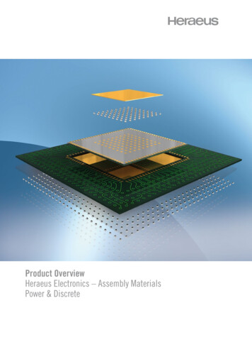
Product OverviewHeraeus Electronics – Assembly MaterialsPower & Discrete
IntroductionContentIntroduction02mAgic Sinter Materials03Solder Wires for Die Attach04Solder Pastes for Die and Clip Attach05Solder Pastes for Bumping06Fluxes and SmartFluxes for Ball and Flip Chip Attach07Water Soluble Solder Pastes for System in Package (SiP)08Adhesives for Die Attach09Solder Pastes for Direct Copper Bonding (DCB)10Welco – Ultra Fine Solder Powder11 The Global Business Unit, Heraeus Electronics – Assembly Materials is thepremier manufacturer of materials for semiconductor assembly / packaging andprinted circuit boards. The business focus is on 3 distinct but related productsegments:n A utomotive and Industrial – Materials for PCB assembly of high reliabilityelectronic circuitsn Power and Discrete – Materials for assembly / packaging of Semiconductors and related technologiesn Powder – Vertically integrated manufacture of Solder Powdersfor every application (Low Alpha, Lead Free, Wafer Bumping, etc.).Our state of the art laboratories feature not only the latest in analytical anddevelopment tools but also utilize the latest manufacturing assembly equipmentso our research and customer application teams can duplicate the customer‘sprocess.This laboratories are linked to our production sites and support customers in their region.47ic107.86Microbond Silver Interconnect2The focus of this brochure is the Power and Discrete segment of Heraeus Electronics – Assembly Materials. This segment specializes in materials designed forthe assembly / packaging of power and discrete semiconductors as well as related technologies such as Die Attach, DCB (Direct Copper Bonded), SiP (Systemin Package), Bumping and Flip Chip Attach to name a few.Key products in this segment include: Solder Wires, Solder Pastes, Conductiveand Non Conductive Adhesives and Fluxes. Additionally, the revolutionary SmartFluxes and mAgic Sinterpaste and Adhesive are featured.
mAgic Sinter MaterialsHeraeus Lead Free Die Attach TechnologyAs a leading supplier of Die Attach materials to the powerelectronics market Heraeus recognized the need for highperformance materials. Our research and developmentteam created a new class of Die Attach materials to meetthis requirement. This novel material technology, utilizingsilver sintering technology, is branded as mAgic (Microbond Ag Interconnect). The product platform consists ofsilver sintering pastes and silver sintering adhesives thatcontain micro-scaled silver particles, which allow a wideprocess and application window. Due to their exceptionalelectrical and thermal performance sinter pastes are suitable for high power density modules. The newly developedsinter adhesives, which are processed as easily as conventional adhesives, can replace solders in low to mediumSeriespower density modules. Compared to lead free solderjoints, sinter adhesives joints exhibit similar electrical andthermal properties and, at the same time, provide increased reliability performance at high operation temperatures.mAgic materials are currently in high volume productionand demonstrate their outstanding performance in highpower modules and converters daily.Thanks to their excellent thermal performance and abilityto withstand elevated operating temperatures, mAgicmaterials allow for increased power densities and higheroperating temperature in packages. mAgic has allowed fora breakthrough in the design of cheaper, lightweight andmore robust devices.ConventionalConductive AdhesivemAgic AdhesivemAgic PasteSolder120 – 175 C180 – 200 C200 – 280 C200 – 350 CMax. Operation Temperature150200 250150Electrical Resistivity (mΩ cm) 0.1 0.05 0.0080.01 – 0.03Thermal Conductivity (W/mK)2–7 30 10020 – 5040/10050/110 2325 – 301–44 35 30Process TemperatureCTE (ppm/K)E-Modulus @ 25 C (GPa)mAgic AdhesiveNo PressureASA47ic107.86Microbond Silver InterconnectmAgic PastePressure AssistedASP043Pressure AssistedASP131No PressureASP295ApplicationDie Attach Component Attach n/an/a Dispensing n/an/a Printing ProcessmAgicPropertiesHalogen Free Lead Free 0 MPa20 MPa10 MPa0 MPaSinting in Air Sintering in N2 n/an/a not needednot needednot needednot needed89%100%100%100%Recom. Sinter PressureCleaningMetal Content afterProcessing (by weight)Compat. Surface FinishesAg Au Pd 3
Solder Wires for Die AttachThe Die Attach process remains a key step in the manufacture of power packages toensure product reliability. With the automotive and aerospace industries setting everhigher reliability requirements, the demands on Die Attach materials are becomingmore and more stringent.Thermal and mechanical fatigue defects in electronic components are caused primarilyfrom successive on/off cycling. To maximize reliability, engineers must identify theoptimum combination of material performance and properties. This is where Microbondmaterial technology makes the difference.To illustrate this advantage we will examine the Die Attach process. The Die Attachjoint has three main functions. In the first place it ensures the mechanical connectionof the die onto the lead frame. Secondly, it enables heat dissipation from the die tothe heat sink and lastly permits electrical contact and transmission.High melting point solder alloys are required for high operating temperature of devices.The Microbond advantage is in a complete portfolio of alloys and materials that are suitedto a wide range of temperature requirements.Specifically doped solder material involves the addition of a minimal amount (ppm range)of wetting enhancing elements. The controlled addition of these substances significantlyimproves the wetting and flowing properties of the alloy. It provides a higher productionyield and reliable results.Standard 5PbSn10Ag2PbIn5Ag5SnAg25Sb10 ApplicationDie AttachProcessWire Dispensing (WD) Patterning with Motorized Pre-Press Module (MPPM) Wire Dispensing with Soft Solder Dispenser (SSD) n/a n/an/an/aPb Freen/an/an/an/an/an/an/a Flux Free PropertiesNo Cleaning Void rate 5 % Excellent Wettingn/a n/an/aSuperior Reliability n/an/a n/a n/aStandard wire diameters are in the range of 10 to 40 mil(0.254 – 1.01 mm). The Microbond advantage is the abilityto control extremely tight wire diameter tolerances thrua sophisticated wire extrusion process. This state of theart process ensures a wire surface that is free of organic4contamination and oxides in order to provide perfect wetting and the lowest void rate possible. Microbond SolderWires guarantee a consistent bondline thickness (BLT) anda very low tilt rate.
Solder Pastes for Die and Clip AttachAs with the Microbond Solder Wire, Microbond SolderPastes come in a wide variety of solder alloys. In addition,vertical integration of the solder powder manufacturingprocess provides the Microbond advantage. The ability toprecisely control alloy purity and achieve the tightest PSD(particle size distribution) ensures the outstandingperformance and high yields that customers demand.The table below illustrates standard Die AttachSolder Paste available. In addition, Microbondproducts are available for special applications andyour Microbond contact can assist in choosing theright product for your process. Die Attach Solder Pastesare packaged in easy to use syringes for a variety ofdispensing systems and provide the following benefits:Excellent dispensing behaviorGood Tackiness & superior soldering propertiesLow VoidingNo CleanSeriesF367RM210RM212Water SolubleRM218DA444DA447CL30-7386ApplicationDie Attach Clip/Bridge Attach Passive Component Attach n/aProcessDispensing Printing n/an/a n/an/an/aPin Transfern/a n/an/an/an/an/aPropertiesHalogen Free (IEC) n/a ActivationL0L0M1L0LOL1H1Superior Wettingn/an/a n/an/a Reflow in Airn/a n/an/an/aReflow in Nitrogen / Forming Gas No CleanOwing to good surface-insulation resistance properties,No Clean solder pastes do not require cleaning, however cleaning with compatible solvents is also possibleif desired.Water SolubleThese pastes feature optimized flux systems that ensureaggressive wetting while maintaining ease of cleanability.Optimum cleaning performance is achieved using hot DIwater promptly after reflow.5
Solder Pastes for BumpingBumping is an advanced packaging technique wheresubstrates or wafers are bumped with Solder Pastes.Spezialized Fluxes are utilized to produce very uniformbumps with the highest accuracy and reliability afterreflow.A critical factor in obtaining the best performance is thesolder powder as it composes 85 – 90 % by weight ofthe bumping paste. Heraeus solder powders for bumpingpastes have exceptional particle size distribution.Achieved by a patented in house technology whichproduces ultrafine powders at a very high yield, Heraeusis the leading producer of sophisticated powders.The solder paste bumping process is a more flexible,faster and cost effective production process comparedto conventional plating or sputtering methods.Bumping PastesVoid rate performanceWater SolubleSeriesF510F590ApplicationSeriesF510 T6OSPCuWafer Bumping Substrate Bumping Stencil Printing Halogen Free (IEC)n/a Superior Wetting SnAg3Cu0.5 SnCn0.7 Type 5 (10 – 25 µm) Type 6 (5 – 15 µm) PropertiesCleanabilityTypical AlloysPowder Types*Low Alpha and Ultra Low Alpha grades are available on request.* Powder types smaller than type 6 are available on request.6Comparable void rate achieved using the same Heraeus lead free reflow profileF590 T6
Fluxes and SmartFluxes for Ball and Flip Chip AttachTacky fluxes are widely used in electronic assembly. Oneof the main applications is the Ball Attach process whichuses mainly water soluble Fluxes. The primary function ofthe material is to hold the ball in place during the reflowand provide improved wetting performance. After this theywill be removed completely from the circuit with a watercleaning process.The SmartFlux, created by the Heraeus developmentteam, improve sicnificantly the missing ball yield.Missing ball appears due to warpage of the substrateduring the reflow process.This new material is a combination of high tackyfluxes and special solder powders. The addition of thepowder prevents the movement of the ball and improvesthe wetting to the substrate surface at the same time.Another application is Flip Chip Attach. For this applicationwater soluble or no clean fluxes are used. Both materialproviding the same basic functionality but the no cleanfluxes will remain on the circuit. Key to no clean fluxperformance is outstanding SIR performance and excellentcompatibility with the underfill process.SmartFlux allows for significantly improved yieldsespecially for high value packages and devices inutilizing copper or tin metallizations.Tacky FluxesSmartFluxNo CleanSeriesWater SolubleNo CleanWater SolubleBD 72FLX 89131NC 5070TF 38Ball Attach n/a Flip Chip Attach WSD 3892WSD 3810-CFFApplicationProcessPrinting Pin Transfer Ball Dip Dispensing n/aPropertiesHalogen Free (IEC) n/aFlux Activity (J-STD)L0L0H1H0L0H1Clear Color of Flux Residues n/an/a n/aCleanability with DI Watern/an/a n/a Superior WettingTackiness n/a n/an/an/an/a Typical AlloysSnAg3Cu0.5Powder TypesType 5* (15 – 28 µm)n/an/an/an/an/a Type 5 (15 – 25 µm)n/an/an/an/a Type 6 (5 – 15 µm)n/an/an/an/a * Type 5 with upper powder size of 28 µm7
Water Soluble Solder Pastes for System in Package (SiP)System in Package (SiP) is an established technologyto provide reasonable costs for the semiconductorminiaturization. This system integrates active and passivecomponents with standard Surface Mount Technology toachieve complex circuits. Continued miniaturization andthe incorporation of 3D integrated modules increase thecomplexity of these packages as well as the functionality.As capabilities and sophistication increases materialselection will play a key role not only in packageperformance but manufacturing yield as well.Heraeus is a major supplier to the SiP Industryand provides a full range of Solder Paste, TackyFluxes and Adhesives. Due to their industry leadingperformance, Heraeus products enable high yieldsand wide process windows which offer potentialcost savings to manufacturers.Water SolubleSeriesF541 HBFF590WL449F510Die Attach Component Attach n/aApplicationProcessPrintingPropertiesHalogen Free (IEC)n/a Flux Activity (J-STD)H1M1M0H1Superior Wetting Reflow in Nitrogen SnAg3Cu0.5 SnSb5 n/an/aSnCu0.7 n/a Type 3 (25 – 45 µm) n/aType 4 (20 – 38 µm) n/aType 5 (15 – 75 µm) n/a Type 6 (5 – 15 µm) n/a Typical AlloysPowder Types8
Adhesives for Die AttachDie Attach Adhesives have a long tradition in thesemiconductor industry. The flexibility of this materialmakes them ideal for attaching different sized die ona variety of substrate materials. The Heraeus portfolioof Die Attach Adhesives provides a wide range of readyto use, single component systems.Heraeus Die Attach Adhesives can improve the productionyield due to their long pot life, wide process window, fastcure, high thermal conductivity and outstanding temperature stability. One special characteristic is less bleedout which enables our customers to decrease the spacebetween bond pads and work with maximum die sizes.Excellent dispensing properties lead to maximum throughput and the lowest cost of ownership.Conductive AdhesivesSeriesPC 3000PC 3070PC 3230Non Conductive AdhesivesPC 3430PC 3600NCA 2NCA 5NCA 6NCA 11ApplicationDie Attach * Flip Chip Attachn/an/an/an/an/an/an/a n/aComponent Attach n/an/an/an/a Dispensing Printing n/an/an/a n/an/a10 min @ 80 CProcessCuring, Conditions and PropertiesRecommended Curing10 min @ 150 C10 min @ 150 C5 min @ 120 C10 min @ 150 C5 min @ 80 C10 min @ 150 C5 min @ 150 C10 sec @ 170 CFast Curingn/an/a n/an/an/a Flexible n/a Pot Life Low Warpage n/a High Thermal Conductivity n/an/an/an/a* max. 5 x 5 mm9
Solder Pastes for Direct Copper Bonding (DCB)so called base plate which supports the heat spreadingand heat transfer to a passive or active cooling system.The majority of DCB modules are used in DC-DC or AC-DCconverters. Those converters are typically used in the fieldof e-mobility and renewable energy. Heat is generated dueto the high power handled by the modules. This heathas to be dissipated efficiently or reduced product lifecycles will be the result. Voids, which hinder good heatdissipation, will be minimized by using a vacuumsoldering process. To further minimize voiding and also– 0,475to guarantee a low level of die tilt, the solder paste– 0,45– 0,425needs to be capable of being printed on large areas– 0,4– 0,375of 100 mm² uniformly and without holes.DCB is the traditional technology used for high powerapplications were currents of 30 A up to several thousandamperes are commonly experienced.DCBs consist of a ceramic core, typically Al2O3, that actsas an insulation layer and thick copper tracks to providean electric path on the top side of the device. In addition,a copper layer is found on the back side of the device.The copper layers usually have a minimum thickness of300μm to ensure a high current carrying capacity.To ensure a good bondability of the circuit in latermanufacturing steps the flux residues have to be easilyto removed. As one of the market leaders of solder pastefor DCB application Heraeus has many years of developinghigh performance materials for DCB applications.Our materials are compatible with the vacuum solderingprocess, provide a outstanding print to print consistencyand are easy to clean.MOSFETs, IGBT and diodes are typically soldered to thetop side of the DCB. The back side may be soldered to aWater SolubleNo CleanSeriesF360F360 C20F825F645WL449Die Attach Component Attach Halogen Free (IEC)n/an/a n/a Flux Activity (J-STD)L0L0L0L0M0Min. Die Tilt Control of Bond Line Thickness Reflow in Nitrogen SnAg3.5 n/a n/a SnAg3.5Cu2.0n/a n/an/an/aSnAg3Cu0.5n/an/an/a n/aApplicationProcessPrintingPropertiesTypical AlloysPowder Types10– 0,35– 0,325– 0,3– 0,275– 0,25– 0,225– 0,2– 0,175– 0,15– 0,125– 0,1– 0,075– 0,05– 0,025–0Type 2.5 (25 – 75 µm) n/an/a Type 3 (25 – 45 µm)n/an/a
Welco – Ultra Fine Solder PowderHeraeus has developed Welco-powders for ultra-finepitch solder paste in various printing applications.The capabilities are ranging from dry film (patented byFCI) to stencil printing. The results of these processes arehigh quality flip chip or pre-soldered flip chip substrates.These solder powders enable pitches down to 60 µm,whereas the printing process represents a more costeffective and flexible bumping method compared toPowdersconventional sputter or plate methods. Advantagesof the Welco technology include a very narrow andadjustable particle-size-distribution, controlled byspeed, process time and geometry of the dispersingtools, as well as very low oxygen contents in eachpowder types.Welco – only registered in USALead freeLead containingSn96.5 Ag3.0 Cu0.5Sn95.5 Ag4.0 Cu0.5Sn99.3 Cu0.7Sn63 Pb37217 – 219 C217 – 225 C227 C183 CType 5 [10 – 25 µm]xxxxType 6 [5 – 15 µm]xxxxType 7 [2 – 11 µm]xxxxType 8 [2 – 8 µm]x**–Low Alpha [ 0.02 cph/cm²]x–xxx Alloys available * under RnDOther alloys and low alpha qualities on request. Purity of all material 99.9 %1200Comparison – Powder Particle Sizes and Specific SurfacesSpecific surface [cm/g]1000Welco The specific surface of the Welco powder is 3 to 6 timeshigher versus classic powders.8006004002000ClassicType 3Type 4Type 5Type 6Powder TypeType 7Type 811
02.2016/VN Layout: data-graphis HET-MarComThe data given here is valid. We reserve the right to make technical alterations.Heraeus ElectronicsHeraeus Deutschland GmbH & Co. KGHeraeusstraße 12-1463450 Hanau, Germanywww.heraeus-electronics.comAmericasPhone 1 610 825 6050electronics.americas@heraeus.comChinaPhone 86 21 3357 5194electronics.china@heraeus.comAsia PacificPhone 65 6571 7677electronics.apac@heraeus.comEurope, Middle East and AfricaPhone 49 6181 35 3069 49 6181 35 3627electronics.emea@heraeus.comThe descriptions and engineering data shown here have been compiled by Heraeus using commonly-accepted procedures, in conjunction with modern testing equipment, and have been compiled as according to the latest factual knowledge in ourpossession. The information was up-to date on the date this document was printed (latest versions can always be supplied upon request). Although the data is considered accurate, we cannot guarantee accuracy, the results obtained from its use, orany patent infringement resulting from its use (unless this is contractually and explicitly agreed in writing, in advance). The data is supplied on the condition that the user shall conduct tests to determine materials suitability for particular application.
Another application is Flip Chip Attach. For this application water soluble or no clean fluxes are used. Both material providing the same basic functionality but the no clean fluxes will remain on the circuit. Key to no clean flux performance is outstanding SIR performance and excellent compatibility with the underfill process.
