Transcription
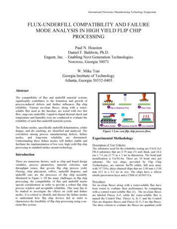
International Electronics Manufacturing Technology SymposiumFLUX-UNDERFILL COMPATIBILITY AND FAILUREMODE ANALYSIS IN HIGH YIELD FLIP CHIPPROCESSINGPaul N. HoustonDaniel F. Baldwin, Ph.D.Engent, Inc. – Enabling Next Generation TechnologiesNorcross, Georgia 30071W. Mike TsaiGeorgia Institute of TechnologyAtlanta, Georgia 30332-0405AbstractThe compatibility of flux and underfill material systemssignificantly contributes to the formation and growth ofprocess-induced defects and further influences flip chipreliability. Various no-clean fluxes, along with a watersoluble flux used as the baseline, are tested with two fastflow, snap cure underfills. Liquid-to-liquid thermal shock andtemperature and humidity tests are conducted to evaluate thereliability of each flux-underfill material system.The failure modes, specifically underfill delamination, solderfatigue, and die cracking, are identified and analyzed. Thecorrelation among process manufacturing defects, failuremodes, and long-term reliability are determined.Understanding these failure modes will further enable andfacilitate the implementation of low cost, high yield flip chipprocessing in standard surface mount technology.IntroductionThere are numerous factors, such as chip and board designvariables, process parameters, material selection, andthroughput issues, that govern flip chip process yield.Fluxing, chip placement, reflow, underfill dispense, andunderfill cure are the processes of flip chip assemblyillustrated in Figure 1. Of the many challenges in flip chipprocessing, the compatibility of flux and underfill meritsspecial consideration in order to provide a robust flip chipprocess window and acceptable reliability. This issue has tobe studied to investigate the effects on yield and failuremodes. It is critical to identify and discuss the failure modesto understand how flip chip devices fail in order tocharacterize the feasibility of flip chip processing using a noclean flux system.Figure 1 Low cost flip chip process flow.Experimental MethodologyDescription of Test VehiclesThe substrates used for the reliability testing are FA10 2x2FR-4 substrates that are 0.79 mm (31 mil) thick, and 14.6cm x 7.6 cm (5.75 in x 3 in) in dimension. The bond padmetallization is Cu/Ni/Au. There are 10 bond sites persubstrate. The test chips, provided by Flip ChipTechnologies, are eutectic Sn/Pb solder, full area arraywith 317 I/Os, daisy-chained chips that are 5.08 mm x 5.08mm (0.2 in x 0.2 in) in size. The chips have a siliconnitride passivation layer and a UBM of Al/NiV/Cu.ProceduresSix no-clean fluxes along with a water-soluble flux havebeen tested to evaluate their performance by comparingwith a control water-soluble flux [1]. The no-clean fluxesare labeled Fluxes A-F, while the water-soluble flux isnamed the Control Flux. Fluxes A, B, C and the ControlFlux are dispense fluxes; and Fluxes D, E, F are dip fluxes.The three criteria to evaluate the fluxes are quadrant yield
International Electronics Manufacturing Technology SymposiumSan Jose, July 2002percentage via electrical continuity testing, interconnectvoiding percentage, and interconnect shear strength via dieshearing. Electrical continuity testing is based on chip,column, and interconnect yields. The solder voids aredetected under X-ray microscopy to observe the number andsize of voids before chip placement and after reflow. Theshear test distinguishes the fluxes by the shear strength suchthat a higher shear force tends to indicate better adhesion andmore robust interconnects [1].The flux evaluation, based on an Archimedean rankingtechnique, determines that Fluxes A, D, F, and the ControlFlux perform better and are utilized for assembliesimplementing two different fast flow, snap cure underfills(labeled Underfills A and B). These assemblies are placed inliquid-to-liquid thermal shock (LLTS) testing andtemperature and humidity (T/H) testing to assess theirreliability with respect to eight different flux-underfillmaterial system combinations [1].Table 1 Underfill material properties.PropertyCTE (ppm/ C)Filler Content (%)Viscosity (cP)Tg (C)Underfill AUnderfill B35408,000130286210,000144The underfills, described in Table 1, are selected because oftheir distinctive difference in material properties and flowcharacteristics. Underfill A has a higher CTE and a lowerfiller content whereas Underfill B has a lower CTE and ahigher filler content.The experimental matrix is presented in Table 2. Thirtyassemblies are built for each material system. An L-shapedispense pattern is employed for Underfill A samples; and aone pass, I-shape dispense pattern for Underfill B samples.For LLTS testing, the samples are subjected to twotemperature baths of extreme temperatures (-55 and 125 C),whereas for T/H testing, the samples are tested under theconditions of 85 C and 85% relative humidity.Electrical continuity of each daisy-chained loop is a means ofdetermining failure. A chip whose resistance exceeds thethreshold of 10% of the original resistance at time zerobefore cycling is considered a failure. In addition, if a sampleis detected with a die crack based on C-SAM analysis, it isalso regarded as a failure, despite that the sample may stillmaintain electrical continuity.Table 2 Experimental matrix.Material Combinations ample SizeSample 30FA30-FB30-Total No. Of Samples240180Testing Conditions55C/125C85C/85%RHContinuity CheckEvery 100 Cycles Every 100 HoursC-SAMEvery 200 Cycles Every 200 HoursLast TestUntil Failure1000 HoursLLTS Results and AnalysisUnderfill AFigure 2 presents the Weibull distribution plot of the LLTSfailure rate of each flux sample with Underfill A. Theresults are summarized in Table 3. In general, the firstfailures of the Underfill A samples occur after only 200cycles. Most of the early life failures are caused by diecracking, discussed below. Flux D demonstrates the bestcompatibility with Underfill A, with a mean time to failureof 1490 cycles, 264 cycles more than the Control samples.Flux F and Flux A excel in terms of solder wetting andyield [1], but they do not perform well in terms ofreliability testing with Underfill A.While most of the other samples fail due to electricalcontinuity loss, numerous test vehicles with Flux F exhibita propensity for die cracking, with several samplescracking after 200 cycles. An additional Weibulldistribution analysis is performed for Flux F samplesexcluding die cracking as a failure mode. It shows that ifdie cracking is neglected, Flux F samples generate a muchhigher reliability life of 1687 cycles. It also has a muchlarger Weibull shape parameter of 10.63, which describesthe slope of the Weibull distribution and is related to thefailure rate.
International Electronics Manufacturing Technology SymposiumSan Jose, July 200299Flux AP e rc e n t F a ile d (% )90Flux D50Flux F10Flux F*Control110100100010000Time to Failure (Cycles)Figure 2 Weibull distribution for Underfill A.Table 3 LLTS testing results for Underfill AFluxUnderfillFirstLast WeibullShapeFailure 02300168710.63* denotes results excluding die cracking as a failure mode.Underfill BThe results for each flux sample with Underfill B aresummarized in Figure 3 and Table 4. Figure 3 presents theWeibull distribution plot that depicts the LLTS failure rate ofeach material system.99Flux AP e r c e n t F a ile d ( % )90Flux D50Flux F10ControlFor Underfill B-Flux A samples, the mean time to failure is824 cycles. It is apparent that this material combination isnot particularly compatible in terms of reliability. On theother hand, Flux D, which is not compatible with UnderfillA, performs well with Underfill B, having a Weibull life of2983 cycles. The Control samples perform very well, witha Weibull life of 4006 cycles.Flux-Underfill CompatibilityComparing the results of these eight material systems,Underfill A works the best with Flux D, with a life of 1490cycles. Underfill B is not particularly compatible withFluxes A and D, but it is compatible with Flux F. UnderfillB-Flux F samples provide the largest number of cycles forthe no-clean process with a mean time to failure of 2983cycles. Underfill B performs well with the water-solubleControl Flux, having a life of 4006 cycles; and with FluxF. This is an indication that Underfill B is capable ofeffectively reducing the CTE mismatch between the chipand the substrate. In fact, the Control Flux-Underfill Bsamples last 2780 cycles longer than the Control FluxUnderfill A samples.Effects of Underfill VoidingIt is found from C-SAM images that there are somesamples that contain underfill voids after cure. Theformation of underfill voids is attributed predominantly tothe dispense pattern, dispense parameters, insufficientunderfill volume, and the flux residue remaining afterreflow. The L-shape dispense pattern might instigate voidsin the center of the chip where the two flow fronts meetand generate shadow voids or capture voids due to flowfront instability (Figure 4).Voids formed with the I-shape dispense pattern aregenerally seen near the edge opposite of the dispensededge, shown in Figure 4. This type of void is generatedbecause the underfill flows along the left and the rightedges faster than through the solder joints in the center.The flow fronts converge near the lower center of the chip,entrapping air and creating capture voids. The justificationof underfill void formation is confirmed by underfill flowcharacterization studies [2].110100100001000Time to Failure (Cycles)Figure 3 Weibull distribution for Underfill B.Table 4 LLTS testing results for Underfill BFluxUnderfillControlADFBBBBFirstLastFailure 82410512983ShapeParameter2.652.922.021.85Another cause is flux residues. Because no cleaningprocedure is employed with the no-clean flux samples,some flux residue can remain around the solder joints oralong the edges of the chip. Such residue can block theunderfill from flowing through the gaps between solderjoints; thus voids can be generated randomly near solderjoints. An example is shown in Figure 5 for Flux A inwhich residues are observed along the chip edges. Thisoccurrence is flux specific and random regardless of thedispense pattern.
International Electronics Manufacturing Technology SymposiumSan Jose, July 2002Shadow VoidsFlux D-Underfill A0 cycle200 cycles2300 cycles3500 cycles4300 CyclesCapture VoidControl Flux-Underfill BColumns 1, 16, 17 FailFigure 4 Underfill voids caused by dispense pattern.Figure 6 C-SAM images of a Control sample with a largeunderfill void.L-shapeI-shapeFigure 5 Underfill voids caused by flux residues.In terms of the impact of underfill voiding on reliability, theeffect is not strictly detrimental to the reliability data, sinceall Underfill A material systems and all but one of theUnderfill B material system survive more than 1000 cycles.In general, samples with underfill voids do not exhibit asignificant impact on reliability. In order to determine itseffect, the Control samples are studied because they do nothave flux residues that can reduce device reliability life.Figure 6 presents the sequential C-SAM images of a ControlFlux sample with Underfill B undergoing LLTS testing. Thissample is selected because of its large underfill void, which isthe worst case process defect caused by the I-shape dispensepattern. Small areas of underfill delamination start after 200cycles, and they are scattered around the chip as the testingcontinues. The solder joints inside the void start toexperience some weakening after 2000 cycles. Delaminationis detected at the bottom right corner after 3500 cycles. Itfinally fails electrically after 4300 cycles at columns 1, 16,and 17, due to delamination and solder fatigue. Note that theregion where the void is present retains electrical continuitydespite the severe solder fatigue as illustrated by appearanceof the white C-SAM signature of the joints in the voidedlocation.Finite element analysis of flip chip assemblies duringthermal cycling performed by Schubert, et al. [3] showsthat the magnitude of the maximum accumulated creepstrain on samples with a small underfill void near thecenter is equivalent to that of samples with no voids.Samples with a big void actually have lower creep strainsbecause the overall stiffness of the assembly is decreased.However, voids can still generate stresses and strainsbecause of the CTE mismatch. As such they can causenearby solder joints to fail sooner because of rapid fatigue[3].LLTS Failure Mode AnalysisThe primary failure modes identified in the LLTS testingare underfill delamination, solder fatigue, and die cracking.The most prevalent failure is delamination at the chippassivation-underfill interface that eventually leads tosolder fatigue failure. Figure 7 shows typical delaminationdetected in reliability testing: column or row delaminationin the spacing between solder joints, bulk (massive)delamination, and delamination around corners or edges ofthe chip. There is also halo delamination, forming a ringlike shape around individual solder joints. Halo defects aretypically caused due to the existence of flux residuesaround the solder, promoting local delamination.Column/Row DelaminationBulk DelaminationHalosFigure 7 Examples of underfill delamination.
International Electronics Manufacturing Technology SymposiumSan Jose, July 2002Solder fatigue cracks, shown in Figure 8, account for most ofthe electrical failures observed in LLTS testing. Underfilldelamination generally leads to local solder fatigue failure inhigh stress regions as the testing progresses. When there is acrack in the solder, an elevated resistance reading or an openloop is found.Solder CrackFigure 8 Solder fatigue cracking.Die cracking is observed in some of the samples. It isdetected via C-SAM images. It appears as a dark line runningthrough or along the edges of a chip. Figure 9 presents threeexamples of die cracks located near the edge of the chip. Diecracks generally originate from the chip edge. They growinside toward the solder joints due to the large stresses andstress risers along the edges of the chip caused by the globalCTE mismatch between the chip and the substrate, bendingeffects at the chip edges, silicon die defect, and assemblywarpage.Table 5 presents the breakdown of failure modes of all theLLTS samples. Notice that delamination that leads to solderfatigue is the most prevalent failure mode in LLTS testing.For Underfill B samples, more than 60% of all samples faildue to delamination/solder fatigue.Sample 1Sample 2XTotal Delamination/DieFailure Solder Fatigue CrackingUnderfill 9%23%55%56%34%21%77%45%44%Underfill 95%72%63%83%0%5%28%37%17%Figure 10 shows an example of delamination that startsfrom the chip-underfill interface, and penetrates towardsthe bulk underfill along the edge of the solder joint. Thisdebonding of underfill is so severe that it actuallypropagates through the underfill layer and into the soldermask and substrate, causing substrate cracking.UnderfillDelaminationSubstrate Crack1100 CyclesFigure 10 Underfill delamination and substrate crackingfound in a Flux D-Underfill B sample.Sample 3XTable 5 LLTS failure modes.FluxUnderfillXXFigure 9 Examples of die cracking failures.For Underfill A samples, die cracking is a commonlydetected failure mode that occurs as early as 200 cycles.For the Flux F samples, 77% of the samples fail due to diecracking. C-SAM and cross-section images of die crackingare shown in Figure 11. In this case, the crack originatesfrom the corner of the chip where the crack is moredefined. It propagates downward and into the bulk of thesilicon until it encounters a uniformly distributed stresslevel and it starts to propagate parallel along that plane.This is an example of an in-plane crack that occurs overtime that is believed to be static fatigue [4]. As the testingcontinues, the crack moves down to the chip passivationand eventually affects the device operation and solderjoints. It is believed that such a crack is generally causedby silicon chip defects from wafer dicing in combinationwith large underfill stresses.
International Electronics Manufacturing Technology SymposiumSan Jose, July 2002AUnderfill CrackChip EdgeChip EdgeFillet CrackFillet Crack(b)AFigure 11 Die cracking found in a Flux D-Underfill Asample.Occasionally, a die crack would occur abruptly afterextensive thermomechanical stress exposure. Figure 12illustrates the C-SAM images of a Flux F-Underfill A samplein which no die cracking is observed after 1400 cycles. But100 cycles later, large cracks across the chip occur. A rowcross-section (plane B-B) image of the cracks is alsopresented to depict the severity of this failure mode.BB1400 CyclesT/H Results and AnalysisThe T/H testing results are summarized in Table 5. Ingeneral, Underfill A samples are more resistant totemperature and humidity exposure. Both Flux A and FluxD samples perform better than the Control samples forboth underfills. The results for Underfill B indicate lowerreliability performance than expected. Moreover, there is aclear indication of the incompatibility of Underfill B withthe Flux D. This outcome demonstrates that evaluatingadditional no-clean fluxes is essential to effectivelydetermine the compatibility of flux and underfill materialsystems.Table 5 T/H results for Underfills A and B.1500 CyclesFigure 12 Die cracking found in a Flux F-Underfill Asample.Underfill cracking is another failure mode observed. Theunderfill cracks are found after samples are cross-sectioned.This failure mode has not been documented in the past forfast flow, snap cure underfills. It is detected in both the bulkunderfill material between solder joints (Figure 13) and in theunderfill fillets (Figure 14). This failure mode is underfillspecific because only Underfill A exhibits such phenomenon,but not Underfill B. A larger amount of filler concentration inunderfill increases its strength and stiffness. Since UnderfillA has a lower filler content with 40%, it tends to crack afterundergoing thermal shock testing.UnderfillVoidsFigure 13 Bulk underfill ed ed90%93%94%57%89%66%The T/H test accelerates moisture absorption andpenetration to flip chip packages through the underfillmaterial. The moisture can deteriorate the adhesion of theunderfill material to the passivation, solder, and soldermask; and thus delamination can be observed especiallyaround the edges and corners of the chip, shown in rFigure 12 Bulk underfill cracking.DelaminationUnderfill VoidFigure 14 Underfill delamination seen in a Flux AUnderfill B T/H sample.
International Electronics Manufacturing Technology SymposiumSan Jose, July 2002In some cases, it also penetrates into the UBM layer andcompromises the adhesion of the UBM to the chip, causingthe UBM pad to lift (Figure 15). Failure in T/H testing istypically a high resistance measurement driven from underfilldelamination, UBM pad lift, and/or micro-cracks in thesolder joints. It has been shown that the delamination aroundthe edges can lead to large stress concentration near thesolder interconnect that eventually fail due tothermomechanical stress.UBM Pad LiftUBM Pad LiftFigure 15 Examples of UBM pad lift failure.ConclusionsRobust and repeatable process windows for no-clean fluxeshave been established to assemble high yield flip chippackages. It is demonstrated that satisfactory reliability isattained with several material systems, with all but oneLLTS material system passing a mean time to failure of1000 thermal shock cycles. The thermal, mechanical, andelectrical phenomena of flux-underfill compatibilitygreatly influence flip chip reliability. The demonstration ofcompatible flux-underfill material systems promotes theapplication of flip chip in surface mount assembly. Thefeasibility of implementing flip chip processing relies onsuch information and reliability data to characterize aspecific process for microelectronic applications. Based onthe results presented, robust flip chip process yield andsatisfactory reliability can be achieved with a no-cleanprocess for commercial applications.References[1] Tsai, W., Houston, P., and Baldwin, D., “Compatibilityof Flux and Underfill Material Systems,” Proceedingsof 2000 International Conference on High-DensityInterconnect and Systems Packaging, April 2000,pp.598-604.[2] Fine, P., Cobb, B., Nguyen, L., “Flip Chip UnderfillFlow Characteristics and Prediction,” Proceedings ofthe 49th Electronic Components and TechnologyConference, 1999.[3] Schubert, A., et al., “Flip Chip Solder JointReliability,” APACK ’99 Symposium on Advances inPackaging, 1999, pp. 234-242.[4] Sylvester, M., et al., “Thermal Cycling Effects onEutectic Flip-Chip Die on Organic Packages,”Proceedings of 2000 International Conference onHigh-Density Interconnect and Systems Packaging,April 2000, pp.438-443.
Fluxing, chip placement, reflow, underfill dispense, and underfill cure are the processes of flip chip assembly illustrated in Figure 1. Of the many challenges in flip chip processing, the compatibility of flux and underfill merits special consideration in order to provide a robust flip chip