Transcription
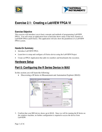
Exercise 2.1: Creating a LabVIEW FPGA VIExercise ObjectiveThis exercise will introduce you to basic concepts and methods of programming LabVIEWFPGA. You will create an application from scratch that shows many of the basic features ofLabVIEW FPGA and R Series. This application will also show the parallelism of a LabVIEWFPGA system.Hands-On Summary Introduce LabVIEW FPGA Learn how to setup and configure a R Series device using the LabVIEW Project Create an FPGA Application that adds two numbers and benchmarks the execution.Hardware SetupPart 0: Configuring the R Series Device in MAXIn this section you will learn the following: Discovering a R Series in Measurement and Automation Explorer (MAX)1. Confirm that your RIO device shows up in MAX. Since we will be running the R Series onthe windows machine, no further configuration is required to access the device fromLabVIEW.Page 1 of 16
Part 1: Developing the FPGA ApplicationIn this section you will learn: Develop, target, download, and run an application on an FPGA.1. Launch LabVIEW 8 and open an Empty Project.2. Click the Save All buttonand save your project as Custom Trigger to the “Intro Demo”folder located on the desktop. Your project should look like this:3. Right-click on My Computer and select New Targets and Devices. This will allow us toadd an FPGA target to our project. Expand the FPGA Target folder, highlight the PCI-7831Rdevice and select OK.Page 2 of 16
4. The LabVIEW Project should look like this:Page 3 of 16
Replace this with new figure5. Developing the LabVIEW FPGA ApplicationIn this section you will: Explore the function palettes while targeted for FPGA.Design an application that adds two numbers and benchmarks the codeThe completed application should look like this:Block DiagramFront Panel6. In the LabVIEW Project Window, right-click on the FPGA target (PCI-7831R) and selectNew VI to start a new LabVIEW FPGA VI (LabVIEW programs are called VirtualInstruments or VI’s). Save this VI as AddFPGA.vi by (File Save As) to signify that thisprogram will be run on the FPGA.Page 4 of 16
New VI7. When the LabVIEW front panel appears, go to the block diagram by selectingWindow Show block diagram.8. Right-click in the white area on the block diagram to display the Functions palette. Click onthe thumb tack icon in the top left corner of the Functions palette to tack it down.FunctionsPallete here9. Navigate to the Help menu and select Show context help. Then browse through theFunctions palette to familiarize yourself with the many math, digital logic, comparison,input/output, math and analysis functions and IP libraries that are available.Browsing the LabVIEW FPGA functions palettePage 5 of 16
10. Go back to the LabVIEW front panel (gray screen), go to View Controls Palette. This willturn the controls Palette ONPage 6 of 16
11. From Controls Palette press “Numeric” button which will envoke Numeric Palette. Nowplace two numeric controls and two numeric indicator in the front panel. You can always goback a level by clicking the upper level in the top left corner (Modern).12. In “Front Panel” rename the controls A and B, and the indicators as C and Execution Time(ticks). It is easier to name the component while placing. To rename right click in the middleof the controls and then click “Properties” and change the name in properties (it is faster toDelete and place them again and name while placing). The Front Panel and Block Diagramsshould look like this now.Page 7 of 16
Page 8 of 16
13. Change their data type to be an Unsigned Byte integer, by right-clicking on each of them andselecting Representation » Unsigned Byte from the shortcut menu. Notice U8 in at thebottom of each icon in Block Diagram (it was I16 initially).14. In the block diagram, add a while loop around the four controls. Tis is done by right clickingand then in Functions Structures While Loop (as shown in screen shot below), makesure the terminals for the controls and indicator are inside the While loop.Page 9 of 16
15. Place the Add function (Functions Numeric) inside the while loop.16. If you do not have the Tools Palette visible, turn ON Tools Palette from View ToolsPalette. In Tools click on “Wire Reel” button and wire A and B to the inputs of the addfunction and wire C to the add function output. Wiring may feel tricky and may require somepractice.Page 10 of 16
A common use of parallelism in LabVIEW FPGA is for benchmarking purposes. Since LabVIEWFPGA implements independent tasks in parallel, we can easily add benchmarking code inparallel to our main application without effecting the performance.17. Right click on the left edge of the While Loop and select Add Shift Register.18. Initialize the shift register by dropping down a numeric constant of zero from the NumericPalette (which is accessible from the Functions Palette Functions Numeric NumericConstant).Page 11 of 16
19. Now, drop down a Tick Count function (Functions Timing), select the counter units to beTicks and keep the size of the internal counter as 32 Bit. Click OK.Configure Tick Count DialogPage 12 of 16
20. Wire the output of the Tick Count function to the shift register on the right side of the WhileLoop21. Drop down a Subtract function on to the block diagram.22. Wire the output of the shift register on the left side of the While Loop and the value of theTick Count function to one inputs of the Subtract function. Wire the output of the Subtractfunction to the indicator labeled Execution Time (ticks).23. Save the VI and project. Click the Run button to start the compile process. The followingwindow will appear:Figure 20. FPGA Build WarningThis is just telling you that compiling the FPGA code can take a long time. Click OK and thecompiling process will begin. After the build process completes, you may run the VI in FPGAinteractive mode. In this mode, the embedded VISA server passes data from the FPGA over thePCI bus to your PC. The update rate in interactive mode is typically limited to about 10 S/s.While the application is compiling, ask one of the instructors if you have any questions orcomments. You’ve worked hard—sit back and enjoy 5-10 minutes of well deserved rest andrelaxation while your LabVIEW FPGA application compiles! If desired, you may read thecomments below that explain the compilation process and other topics that may be of interest.Figure 21. Snapshot during FPGA compilationPage 13 of 16
Understand the LabVIEW FPGA Compilation ProcessThe LabVIEW FPGA Module uses an industry-standard Xilinx ISE compiler. First, yourgraphical LabVIEW FPGA code is translated to text-based VHDL code. At this time, theGenerating Intermediate Files dialogue is displayed. Then the Xilinx ISE compiler tools areinvoked and the VHDL code is optimized, reduced, and synthesized into a hardware circuitrealization of your LabVIEW design. This process also applies timing constraints on the circuitdesign that ensure an efficient use of FPGA resources (sometimes called “fabric”).A great deal of optimization is performed during the compilation process to reduce digital logicand create an optimal implementation of the LabVIEW application. The end result is a highlyoptimized silicon implementation that provides true parallel processing with the performance andreliability benefits of dedicated hardware circuitry. Since there is no operating system on theFPGA chip, the code is implemented in a way that ensures maximum performance and reliability.The end result is a bit stream file that is loaded into your LabVIEW FPGA .VI file. When you runthe application, the bitstream is loaded into the FPGA chip to configure the gate array logic.While the application is running on the FPGA, data for the front panel controls and indicators ispassed over the network several times per second to enable Interactive Mode testing of theapplication. Later we will build a real-time host interface to the application that enables highspeed data transfer and interrupt synchronization between the floating-point host processor andinteger-based FPGA chipset.NOTE: If you disconnect during the compilation, you will need to run the application once whiletargeted to the FPGA in order to load the bitstream into the FPGA VI file from the compileserver.FPGA Clock SpeedBy default, the FPGA clock runs at 40 MHz. This means that one Tick of the FPGA clock is equalto 25 nanoseconds. By changing the compile options, you can increase the FPGA clock speed upto 200 MHz (5 nanoseconds). There are some drawbacks to using higher clock speeds that youshould be aware of before changing the compile option. For more information, refer to theCompactRIO Technical Developers Library by visiting (http://www.ni.com/compactrio) or clickthe Help button on the Target Build Options menu.Understanding the Compilation ReportA SLICE is a collection of logic components on the FPGA. The percentage shown is thepercentage of the FPGA used. As the FPGA reaches greater than 90% usage, the compilerperforms more optimization to make the most efficient use of resources. For simple applications,the compiler does not “try” very hard to optimize, as it does not need to make efficient use ofFPGA resources. For this reason, you may be able to fit more onto the FPGA than this reportwould lead you to believe.Page 14 of 16
Debugging your FPGA Algorithms before CompilationBecause LabVIEW FPGA uses the same high level LabVIEW source code that is used on allLabVIEW targets, you can execute the same code on any processor in a functionally equivalentmanner. This makes LabVIEW a powerful universal programming language for rapiddevelopment of embedded systems. Although the execution timing will be different whenimplemented on the FPGA, the control logic and integer math functionality is the sameregardless of how the code is targeted. When running LabVIEW FPGA code in Windows, you canuse breakpoints, probes, highlight execution mode and other standard debugging tools to validatethe FPGA code. While working in Windows, you can enable the LabVIEW FPGA palette view byclicking the options button at the top-right corner of your functions palette and selecting FPGAHardware in the Palette View menu.When the compiler is complete, the compile report will be generated. This report shows the startand end compilation time, the number of SLICEs used, a compiled clock rate (40 MHz), and anestimated maximum clock rate.Figure 22. Build ReportA SLICE is a collection of logic components on the FPGA. The percentage shown is thepercentage of the FPGA used. In most cases, you can actually fit more onto the FPGA than thisreport would lead you to believe. For simple applications, the compiler does not “try” very hardto optimize, as it does not need to make efficient use of FPGA resources. The compiler will beginto optimize the compiled code when 95% of the FPGA resources are used.24. Click OK to close the build report. The FPGA VI will begin to run automatically. Adjust theanalog output (AO 0) voltage and observe the reaction of the system.25. Click Stop Server to close the compile server.26. Run the VI and watch how it adds the two numbers. You should also notice that the codetakes 6 ticks (or 150 nanoseconds) to execute. Remember we selected an Unsigned Byterepresentation for the controls and indicators. Therefore each control has a range 0-255.Since the indicator also has the same 8 bit range notice what occurs when 2 large numbers arePage 15 of 16
added together. For example, 240 120 returns 104 as a result. This is due to overflow andoccurs when the result does not have enough bits to store the result. There are special nodesfound in the Functions Numeric Saturation Arithmetic palette that can be used to handlethese types of situations. We will discuss these a little later in the lesson.27. After you have run and tested the code close the application and the Project Manager.ALL STAR (OPTIONAL)28. Now open the precompiled example found in the project named Exercise 21.pjt in theSolutions folder. The VI you should open is named Ex 2 1 optional.vi.29. Looking at the block diagram you will notice that we added a subtraction task to the VI. Runthis VI and you will notice that the execution time is still 6 ticks. The execution time remainsthe same because the addition and subtraction tasks are performed in parallel.Page 16 of 16
Because LabVIEW FPGA uses the same high level LabVIEW source code that is used on all LabVIEW targets, you can execute the same code on any processor in a functionally equivalent manner. This makes LabVIEW a powerful universal programming language for rapid development of embedded systems. Although the execution timing will be different when