Transcription
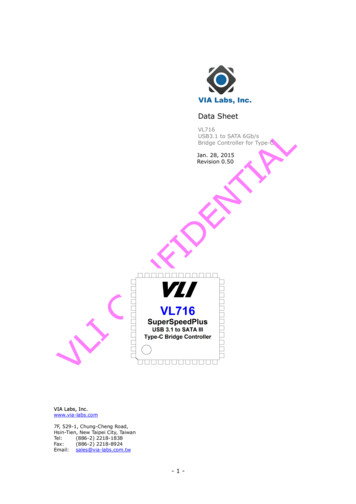
Data SheetVL716USB3.1 to SATA 6Gb/sBridge Controller for Type-CJan. 28, 2015Revision 0.50VIA Labs, Inc.www.via-labs.com7F, 529-1, Chung-Cheng Road,Hsin-Tien, New Taipei City, TaiwanTel:(886-2) 2218-1838Fax:(886-2) 2218-8924Email: sales@via-labs.com.tw-1-
VL716 USB3.1 to SATA 6Gb/s Bridge Controller for Type-CRevision y release-2-
VL716 USB3.1 to SATA 6Gb/s Bridge Controller for Type-CTable of ContentsRevision History . 2Table of Contents . 3List of Figures . 3List of Tables . 3Product Features . 4VL716 System Overview . 5Pinout. 6Pin List . 7Pin Descriptions . 8Signal Type Definition . 8Serial ATA Interface . 8USB 3.0 Interface . 8USB 2.0 Interface . 8Type-C Interface . 9Serial EEPROM Interface. 9Analog Command Block . 9General Purpose I/O and Miscellaneous . 10Test Pin . 10Power and Ground . 10Electrical Specification . 11Package Mechanical Specifications. 19Package Top Side Marking . 20Ordering Information . 20List of �––VL716 Block Diagram . 5VL716 QFN-48 Pin Diagram . 625MHz Crystal equivalent circuit and spec requirement . 12QFN 48L 6x6x0.85 mm Mechanical Specification . 19VL716 Package Top Side Marking . 20List of TablesTable 1 – VL716 QFN-48 Pin List . 7-3-
VL716 USB3.1 to SATA 6Gb/s Bridge Controller for Type-CProduct FeaturesVL716USB3.1 to SATA 6Gb/s Bridge Controller for Type-C ConnectorSuperSpeedPlus USB (10Gb/s) and High-Speed USB (480Mb/s)– Compliant to Universal Serial Bus 3.1 Specification Revision 1.0– Compliant to Universal Serial Bus Specification Revision 2.0– Mass Storage Class Bulk-Only Transport (BOT)– USB Attached SCSI Protocol (UASP) for streaming– Integrated in-house SuperSpeedPlus PHY and USB2.0 PHYSerial ATA 6Gb/s, 3Gb/s and 1.5Gb/s– Compliant to Serial ATA Specification Revision 3.1– Integrated in-house SATA 6Gb/s PHY– RBC command conversion for ATA device– MMC-2 command pass-through to ATAPI– Support 48-bit LBA– Support multiple LUNFast 8051 Macro cell 80C32-Compatible Microcontroller– Standard 1T 8051 instruction setUSB Type-C connector support– CC1/CC2 cable orientation detection logic– Two sets of SuperSpeed USB signal pins to enable plug flipping featureBuilt-in Voltage Regulators– 5.0V to 3.3V LDO– 5.0V to 1.2V switching DC-DCGPIOs for Special Function Usage– 6 GPIOs for customer special usage– 2 dedicated BUSY/POWER LED indicatorsMisc– Support device power down function– Support external SPI flash for firmware upgradeSoftware– Support Microsoft Windows 8, Windows 7, Vista, XP– Support Mac OS 10.X– Support various Linux kernelsPhysical– QFN 48L green package (6x6x0.85 mm)Certification–USB-IF SuperSpeedPlus Certified: TBD-4-
VL716 USB3.1 to SATA 6Gb/s Bridge Controller for Type-CVL716 System OverviewVIA Lab’s VL716 is a high performance, low power single chip USB 3.1 to SATA 6Gb/s bridge controllerwith USB type-C connector support designed for new generation external storage devices that connectingHard Disk Drive (HDD), Solid-State Drive (SSD), and Optical Disc Drive (ODD). Its integrated in-houseUSB 3.1 PHY enables VL716 to run in USB SuperSpeedPlus, Super-Speed, High-Speed, and Full-Speedmodes. Supporting USB mass storage class Bulk-Only Transport (BOT), VL716 based devices can work onWindows 8, Windows 7, Vista, XP, Mac OS X and various Linux kernels without additional driver. BesidesBulk-Only Transport, VL716 also support USB Attached SCSI Protocol (UASP) that allowing mass storagecommand queuing and out of order data transfers to further enhance read/write performance. Itsintegrated in-house SATA 6Gb/s host controller can work with all SATA based storage devices and canconnect at SATA 6Gb/s, SATA 3Gb/s, or SATA 1.5Gb/s automatically. Built-in CC1/CC2 cable orientationdetection circuits and two sets of SuperSpeed USB signal pins can support USB type-C receptacle nativelyto enable plug flipping feature without any extra cost.Built-in all required linear and switching voltage regulators, highly integrated VL716 work perfectly withsingle power input from USB 5V bus power to save customer BOM cost. 6 GPIO pins are available for pushbutton, operation LEDs, device power down control, and other special usage. The SPI interface cansupport external flash for firmware upgrades or additional software enhancements. VL716 is available inQFN 48L (6x6x0.85 mm) green packages to fit small form-factor design supporting USB type-Creceptacle.Figure 1 – VL716 Block Diagram-5-
VL716 USB3.1 to SATA 6Gb/s Bridge Controller for Type-CPinoutFigure 2 – VL716 QFN-48 Pin Diagram-6-
VL716 USB3.1 to SATA 6Gb/s Bridge Controller for Type-CPin ListTable 1 – VL716 QFN-48 Pin ListPinPin NamePinPin B3TXP142BUSYIND19U3TXVDD1243PWRIND20USB3RXP44SPI CS21USB3RXN45SPI Q22USB3RXN146SPI CLK23USB3RXP147SPI D24U3RXVDD1248TESTEN-7-
VL716 USB3.1 to SATA 6Gb/s Bridge Controller for Type-CPin DescriptionsSignal Type DefinitionNameTypeSignal DescriptionInputIA standard input-only signalOutputOA standard active driverInput/OutputI/OA bi-directional signalAnalog biasABIASAnalog bias or reference signal. Must be tied to external resistorand/or capacitor bias networkPowerPWRA power pinGroundGNDA ground pinSerial ATA InterfacePin NameSARXPQFN48I/O3ISignal DescriptionSATA Port Differential Receive Data SARXN4ISATA Port Differential Receive Data -SATXP7OSATA Port Differential Transmit Data SATXN6OSATA Port Differential Transmit Data -SATXVDD128PWRAnalog 1.2VSARXVDD125PWRAnalog 1.2VQFN48I/OUSB 3.0 InterfacePin NameUSB3RXP20ISignal DescriptionUSB 3.0 Port0 Differential Receive Data USB3RXN21IUSB 3.0 Port0 Differential Receive Data -USB3TXP15OUSB 3.0 Port0 Differential Transmit Data USB3TXN16OUSB 3.0 Port0 Differential Transmit Data -USB3RXP123IUSB 3.0 Port1 Differential Receive Data USB3RXN122IUSB 3.0 Port1 Differential Receive Data -USB3TXP118OUSB 3.0 Port1 Differential Transmit Data USB3TXN117OUSB 3.0 Port1 Differential Transmit Data -U3RXVDD1224PWRAnalog 1.2VU3TXVDD1219PWRAnalog 1.2VQFN48I/OSignal Description26I/OUSB 2.0 Bus Data Plus (D )USB 2.0 InterfacePin NameDPDM27I/OUSB 2.0 Bus Data Minus (D–)VCCU25PWRAnalog 3.3V-8-
VL716 USB3.1 to SATA 6Gb/s Bridge Controller for Type-CType-C InterfacePin NameQFN48I/OSignal DescriptionCC129I/OConfiguration Channel 1CC228I/OConfiguration Channel 2QFN48I/OSignal Description44OSerial Flash Chip EnableSPI D47OSerial Flash Data InputSPI Q45ISerial Flash Data OutputSPI CLK46OSerial Flash ClockSerial EEPROM InterfacePin NameSPI CSAnalog Command BlockPin NameQFN48I/OOSCXI12I25M crystal inputOSCXO13O25M crystal outputREXTLDOVDD5Signal Description9ABIASConnect to external resistor10PWR5.0V voltage input for 5V to 3.3V LDOLDOVDD33O11O3.3V voltage output for 5V to 3.3V LDODCVDD536PWR5.0V voltage input for DC2DC regulatorLX37ODCGND38GNDGround for DC2DC regulatorDCVCC1239PWR1.2V voltage input for core powerOSCVDD1214PWROscillator analog 1.2V1.2V voltage output for DC2DC regulator-9-
VL716 USB3.1 to SATA 6Gb/s Bridge Controller for Type-CGeneral Purpose I/O and MiscellaneousPin NameQFN48I/OSignal DescriptionBUSYIND42OBusy LED Indicator, including PWMTypical driving current 15.8mA @ 0.4V & 26.5mA@ 2.4VPWRIND43OPower LED Indicator, including PWMTypical driving current 15.8mA @ 0.4V & 26.5mA@ 2.4VRESET41IExternal Chip ResetGPIO 12I/OGeneral Purpose I/O (15.8mA @ 0.4V & 26.5mA @2.4V in output mode)Default: Device power down controlGPIO 21I/OGeneral Purpose I/O, including PWM (15.8mA @0.4V & 26.5mA @ 2.4V in output mode)Default: USB3.1/USB2.0 mode indicatorGPIO 532I/OGeneral Purpose I/O (15.8mA @ 0.4V & 26.5mA @2.4V in output mode)Default: Push button trigger pinGPIO 634I/OGeneral Purpose I/O (15.8mA @ 0.4V & 26.5mA @2.4V in output mode)Default: USB cable power detectGPIO 733I/OGeneral Purpose I/O (15.8mA @ 0.4V & 26.5mA @2.4V in output mode)Default: Device write protect controlGPIO 831I/OGeneral Purpose I/O (15.8mA @ 0.4V & 26.5mA @2.4V in output mode)Default: Push button status indicatorQFN48I/O48ISignal DescriptionTest Mode EnableDo not connect for normal operation.Internal pull downPin NameQFN48I/OVCC3335, 40PWRDigital IO power 3.3VVDD12I30PWRDigital Core power 1.2VTest PinPin NameTESTENPower and GroundSignal Description- 10 -
VL716 USB3.1 to SATA 6Gb/s Bridge Controller for Type-CElectrical SpecificationAbsolute Maximum RatingSymbolParameterMinMaxUnitTSTGStorage Temperature-55125 CNote—TAAmbient Temperature070 C—VDD33Power Supply Voltage-0.53.69V—VDD50Input Voltage-0.55.5V—VOOutput Voltage at anyoutput-0.5VCC 0.5V—VESDElectrostatic Discharge—2kVHuman Body ModelNote: Stress above conditions may cause permanent damage to the device.Functional operation of this device should be restricted to the conditions described.Operating ConditionsSymbolParameterMinTypMaxVCC33Digital IO power 3.3V3.03.33.6UnitVLDOVDD55V to 3.3V LDO 5V PowerInput4.555.5VDCVDD55V to 1.2V DC2DC 5VPower Input4.555.5VVDD12IDigital Core power 1.2V1.081.21.36VDGNDGround—0—VMaxUnitGeneral IO DC CharacteristicsSymbolParameterMinNoteVILInput Low Voltage-0.300.8V—VIHInput High Voltage2.03.6V—VOLOutput Low Voltage—0.4VIOL 15.8mAVOHOutput High Voltage2.4—VIOH 26.5mAIILInput Leakage Current— /-10µA0 VIN VCCIOZTristate Leakage Current— /-10µA0 VOUT VCCInternal 5V to 1.2V DC/DC ConverterParameterMinTyp.MaxUnitInput Voltage4.55.05.5VOutput Voltage1.141.21.26VMax. Output CurrentTBDTBDmAOutput Voltage Tolerance /- 5%NoteInternal 5V to 3.3V LDO RegulatorParameterMinTyp.MaxUnitInput Voltage4.55.05.5V- 11 -Note
VL716 USB3.1 to SATA 6Gb/s Bridge Controller for Type-COutput Voltage3.1353.33.465VMax. Output CurrentTBDTBDmAOutput Voltage Tolerance /- 5%External Crystal Electrical CharacteristicsPlease refer to the Figure 4.SymbolParameterFLNormal FrequencyMinTypOscillation Mode-30Aging-5Loading CapacitanceC0Shunt CapacitanceRrEffective ResistanceUnitMHzFundamentalFrequency ToleranceCLMax2530ppm5ppm201pf37pf50ohmsFigure 3 – 25MHz Crystal equivalent circuit and spec requirementUSB Full Speed DC/AC CharacteristicsSymbolParameterMinVFSIHFull-speed Input High2.0VFSILFull-speed Input LowVFSCMDifferential CommonMode VoltageVFSOLVNote—0.8V—0.82.5V—Full-speed Output Low0.00.3V—VFSOHFull-speed Output High2.83.6V—TFSRFull-speed Rise Time420ns—TFSFFull-speed Fall Time420ns—VFSCRSFull-speed Output SignalCrossover VoltageMaxUnit1.32.0V—USB High Speed DC/AC speed squelchdetection threshold100150mVNote—VHSCMHigh-speed data signalingcommon mode voltage-50500mV—VHSOIHigh-speed idle level-1010mV—VHSOHHigh-speed data high360440mV—- 12 -
VL716 USB3.1 to SATA 6Gb/s Bridge Controller for Type-CVHSOLHigh-speed data low-1010mV—VCHIRPJChirp J level7001100mV—VCHIRPKChirp K level-900-500mV—ZHSDRVDrive output resistance40.549.5Ω—THSRHigh-speed Rise Time500THSFHigh-speed Fall Time500ps—ps—USB SuperSpeedPlus TX RX CharacteristicsTBDUSB Super Speed TX PDifferential p-p Tx swing0.81.2VNote—VTX-DE-RATIOTx de-emphasis3.04.0dB—RTX-DIFF-DCDC differential impedance72120Ω—VTX-RCV-DETECTThe Voltage Changeallowed during ReceiverDetection0.6V—TTX-EYETransmitter EyeUI—TTX-DJ-DDTx Deterministic Jitter0.205UI—RTX-DCTransmitter DC CommonMode Impedance1830Ω—VTX-DC-CMTransmitter DC CommonMode Voltage02.2V—VTX-CM-AC-PP-ACTx AC Common ModeVoltage -DC0.625Electrical Idle DifferentialP-P Output Voltage010mV—DC Electrical IdleDifferential OutputVoltage010mV—NoteUI does not accountfor SSC causedvariationsDC impedancelimits are needed toguarantee ReceiverdetectMeasured withrespect to groundover a voltage of500mV maximumUSB Super Speed RX Characteristics (5.0 GT/s)SymbolParameterMinMaxUnitUIUnit Interval199.94200.06psR RX - DCReceiver DC commonmode impedance1830ΩR RX - DIFF - DCDC differential impedance72120ΩZRX - HIGH - IMP - DC - POS DC Input CM InputΩ25kImpedance for V 0during Reset or powerdown- 13 -Rx DC CMimpedance with theRx terminations notpowered, measuredover the range 0 –500mv with respectto ground
VL716 USB3.1 to SATA 6Gb/s Bridge Controller for Type-CVRX - LFPS - DET - DIFFp-pLFPS Detect Threshold100VRX -DIFF-PP -POST -EQDifferential Rxpeak-to-peak voltage30t RX - TJMax Rx inherent timingerror0.45UIt RX - DJ - DDMax Rx inherentdeterministic timingerror0.3UIC RX-PARASITICRx input capacitance forreturn loss1.1pfVRX - CM - AC - PRx AC common modevoltage150mVPeakVRX-CM-DC-ACTIVE- Rx AC common mode200mVPeakIDLE- DELTA- P300mVmVvoltage during the U1 toU0 transitionBelow the minimumis noiseMust wake upabove themaximumMeasured after theRx EQ function(Section 6.8.2)Measured after theRx EQ function(Section 6.8.2)Maximum Rxinherentdeterministictiming errorMeasured at Rxpins into a pair of50 Ω terminationsinto groundIncludes Tx andchannelconversion, ACrange up to 5 GHzMeasured at Rxpins into a pair of50 Ω terminationsinto groundIncludes Tx andchannelconversion, ACrange up to 5 GHzSATA TX CharacteristicsSymbolParameterMinMaxUnitZdiffTXTX Pair DifferentialImpedance85115OhmZs-eTXTX Single-EndedImpedance40RL DD11,TXTX Differential ModeReturn Loss(150MHz-300MHz)14dBTX Differential ModeReturn Loss(300MHz-600MHz)8dBTX Differential ModeReturn Loss(600MHz-1.2GHz)6dBTX Differential ModeReturn Loss(1.2GHz-2.4GHz)6dBTX Differential ModeReturn Loss(2.4GHz-3.0GHz)3dBTX Differential ModeReturn Loss(3.0GHz-5.0GHz)1dBTX Differential ModeReturn Loss Start forslope for Gen3Min at300MHz is 14dBRL DD11,TX- 14 -NoteOnly for Gen2i
VL716 USB3.1 to SATA 6Gb/s Bridge Controller for Type-CSlope of TX DifferentialMode Return Loss forGen3-13dB/decTX Differential ModeReturn Loss MaxFrequency for Gen3RL CC11,TXRL DC11,TXVdiffTXMax is 3GHzTX Common Mode ReturnLoss (150MHz-300MHz)8dBTX Common Mode ReturnLoss (300MHz-600MHz)5dBTX Common Mode ReturnLoss (600MHz-1.2GHz)2dBTX Common Mode ReturnLoss (1.2GHz-2.4GHz)1dBTX Common Mode ReturnLoss (2.4GHz-3.0GHz)1dBTX Common Mode ReturnLoss (3.0GHz-5.0GHz)1dBTX Impedance Balance(150MHz-300MHz)30dBTX Impedance Balance(300MHz-600MHz)20dBTX Impedance Balance(600MHz-1.2GHz)10dBTX Impedance Balance(1.2GHz-2.4GHz)10dBTX Impedance Balance(2.4GHz-3.0GHz)4/10dBTX Impedance Balance(3.0GHz-5.0GHz)4dBTX Impedance Balance(5.0GHz-6.5GHz)4TX Differential OutputVoltage400600mVppdFor Gen1TX Differential OutputVoltage400700mVppdFor Gen2TX Differential OutputVoltage200900mVppdFor Gen3Only for Gen2iFor Gen3i is 10dBOnly for Gen3iUIVminTXTXMinimumVoltageMeasurement Interval0.450.55UIt 20-80TXTX Rise/Fall Time100273psTX Rise/Fall Time67136psFor Gen2TX Rise/Fall Time3380psFor Gen3For Gen1t skewTXTX Differential Skew20psVcm,acTXTX AC Common ModeVoltage50mVp-pTX AC Common ModeVoltage 3 GHz Max26dBmV(rms)For Gen3TX AC Common ModeVoltage 6 GHz Max30dBmV(rms)For Gen3D vdiffOOBOOB Differential Delta25mVD vcmOOBOOB Common Mode Delta50mVR/FbalTX Rise/Fall Imbalance20%Only for Gen2AmpbalTX Amplitude Imbalance30%Only for Gen2- 15 -
VL716 USB3.1 to SATA 6Gb/s Bridge Controller for Type-CTJ at Connector Clk-DatafBAUD/500 JTF Defined0.37UIFor Gen1/Gen2DJ at Connector Clk-DatafBAUD/500 JTF Defined0.19UIFor Gen1/Gen23.1MHzFor Gen1/Gen23.5dBFor Gen1/Gen2Jitter Transfer FunctionBandwidth (D24.3,highpass -3dB)1.1Jitter Transfer FunctionPeakingJitter Transfer FunctionLow FrequencyAttenuation6975dbFor Gen1/Gen2Jitter Transfer FunctionBandwidth (D24.3,highpass -3dB)2.26.2MHzFor Gen33.5dBFor Gen341.2dbFor Gen3TJ(10-12)before and afterCIC,Clk-Data JTF Defined0.52UIFor Gen3TJ(10-6)before and afterCIC,Clk-Data JTF Defined0.46UIFor Gen3UnitmVppdNoteJitter Transfer FunctionPeakingJitter Transfer FunctionLow FrequencyAttenuation35.2SATA RX CharacteristicsSymbolVdiffRXt 20-80RXt skewRXVcm, acRXf cm, acRXParameterGen1 RX DifferentialInput VoltageGen2 RX DifferentialInput VoltageGen3 RX DifferentialInput VoltageMin240Max6002407502401000Gen1 RX Rise/Fall time100273psGen2 RX Rise/Fall timeGen2 RX Rise/Fall timeGne2 RX DifferentialSkewGen3 RX DifferentialSkewRX AC Common ModeVoltageRX AC Common ModeFrequencyGen1 TJ at Connector,Data-Data, 5UIGen1 DJ at Connector,Data-Data, 5UIGen1 TJ at Connector,Data-Data, 250UIGen1 TJ at Connector,Data-Data, 250UIGen2 TJ at UI0.6UI0.35UI0.46UI0.35UI0.60UIf BAUDClk-Data,/10Gen2 DJ at Connector,f BAUDClk-Data,/10Gen2 TJ at Connector,Clk-Data,f BAUD/500- 16 -
VL716 USB3.1 to SATA 6Gb/s Bridge Controller for Type-CGen2 DJ at Connector,0.42UI0.60UIf BAUD /500Gen3TJ after CICGen3RJ beforeCICZ diffRXZs-eRXRLDD11,RXClk-Data,Clk-Data JTF DefinedMFTP Clk-Data JTFDefinedRX Pair DifferentialImpedanceRX single-endedImpedanceGen2i/m RX DifferentialMode Return Loss(150MHz-300MHz)Gen2i/m RX DifferentialMode Return Loss(300MHz-600MHz)Gen2i/m RX DifferentialMode Return Loss(600MHz-1.2GHz)Gen2i/m RX DifferentialMode Return Loss(1.2GHz-2.4GHz)Gen2i/m RX DifferentialMode Return Loss(2.4GHz-3.0GHz)Gen2i/m RX DifferentialMode Return B1dBGen3i RX Differential ModeReturn Loss(min @ 300MHz)Gen3i Slop of RX DifferentialMode Return Loss18VthreshUI OOBdB-13Gen3i RX Differential ModeReturn Loss max frequencyRL CC11OhmdB/dec6.0GHzGen2i/m RX Common ModeReturn Loss (150MHz-300MHz)5dBGen2i/m RX Common ModeReturn Loss (300MHz-600MHz)5dBGen2i/m RX Common ModeReturn Loss (600MHz-1.2GHz)2dBGen2i/m RX Common ModeReturn Loss (1.2GHz-2.4GHz)1dBGen2i/m RX Common ModeReturn Loss (2.4GHz-3.0GHz)1dBGen2i/m RX Common ModeReturn Loss (3.0GHz-5.0GHz)1dBGen1 OOB Signal DetectionThreshold50200mVppdGen2/3 OOB Signal DetectionThreshold75200mVppdUI During OOB Signaling646.67686.67psCOMINIT/COMRESET/COMWAKE Transmit Burst Length160160UI OOBCOMINIT/COMRESET TransmitGap Length480480UI OOBCOMWAKE Transmit GapLength160160UI OOBCOMWAKE Gap DetectionWindow55175ns- 17 -
VL716 USB3.1 to SATA 6Gb/s Bridge Controller for Type-CCOMINIT/COMRESET GapDetection Window175- 18 -525ns
VL716 USB3.1 to SATA 6Gb/s Bridge Controller for Type-CPackage Mechanical SpecificationsQFN-48 Pb-free Maximum Temperature for IR ReflowParameterMaximum Temperature TpMax Time within 5 C of TpValue25030Unit CsecondsFigure 4 – QFN 48L 6x6x0.85 mm Mechanical Specification- 19 -
VL716 USB3.1 to SATA 6Gb/s Bridge Controller for Type-CPackage Top Side MarkingQ4: QFN48 PackageVLIVL716-Q4YYWW: Date code(YY Year; WW Week)YYWWTE0XXXXXXXXPackage substanceT True greenIdentification CodeE0 XXXXXXXXRevision CodeInternal codeFigure 5 – VL716 Package Top Side MarkingOrdering InformationPart NumberDescriptionPackageVL716-Q4USB3.1 to SATA 6Gb/s bridge for Type-C48-pin QFN (6x6mm)- 20 -
VL716 USB3.1 to SATA 6Gb/s Bridge Controller for Type-CVIA Labs, Inc.www.via-labs.com7F, 529-1, Chung-Cheng Road,Hsin-Tien, New Taipei City, TaiwanTel:(886-2) 2218-1838Fax:(886-2) 2218-8924Email: sales@via-labs.com.twCopyright 2010 VIA Labs, Inc. All Rights Reserved.No part of this document may be reproduced, transmitted, transcribed, stored in a retrieval system,or translated into any language, in any form or by any means, electronic, mechanical, magnetic,optical, chemical, manual or otherwise without the prior written permission of VIA Labs, Inc. Thematerial in this document is for information only and is subject to change without notice. VIA Labs,Inc. reserves the right to make changes in the product design without reservation and without noticeto its users.All trademarks are the properties of their respective owners.No license is granted, implied or otherwise, under any patent or patent rights of VIA Labs, Inc. VIALabs, Inc. makes no warranties, implied or otherwise, in regard to this document and to the productsdescribed in this document. The information provided by this document is believed to be accurateand reliable as of the publication date of this document. However, VIA Labs, Inc. assumes noresponsibility for any errors in this document. Furthermore, VIA Labs, Inc. assumes no responsibilityfor the use or misuse of the information in this document and for any patent infringements that mayarise from the use of this document. The information and product specifications within this documentare subject to change at any time, without notice and without obligation to notify any person of suchchange.- 21 -
- Compliant to Universal Serial Bus 3.1 Specification Revision 1.0 - Compliant to Universal Serial Bus Specification Revision 2.0 - Mass Storage Class Bulk-Only Transport (BOT) - USB Attached SCSI Protocol (UASP) for streaming - Integrated in-house SuperSpeedPlus PHY and USB2.0 PHY Serial ATA 6Gb/s, 3Gb/s and 1.5Gb/s


