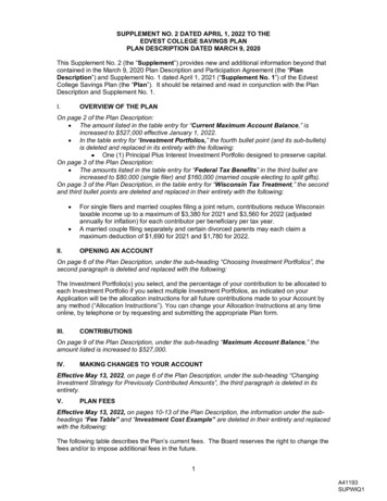
Transcription
This is a preview of "IPC HDBK-001H-2021". Click here to purchase the full version from the ANSI store.IPC-HDBK-001HHandbook and Guide toSupplement J-STD-001Developed by the IPC-HDBK-001 Task Group (5-22F) of the Assemblyand Joining Committee (5-20) of IPCSupersedes:IPC-HDBK-001F - February 2016IPC-HDBK-001E - February 2012IPC-HDBK-001 w/Amendments1 & 2 - October 2005IPC-HDBK-001 w/Amendment 1 December 2000IPC-HDBK-001 - March 1998Users of this publication are encouraged to participate in thedevelopment of future revisions.Contact:IPC
This is a preview of "IPC HDBK-001H-2021". Click here to purchase the full version from the ANSI store.January 2021IPC-HDBK-001HTable of ContentsGENERAL . 10.10.1.10.1.2Scope . 1Purpose . 10.2FORMAT (Using This Handbook) . 11.0GENERAL . 31.11.21.3Scope . 3Purpose . 3Classification . 31.41.4.11.51.5.11.5.21.5.3Measurement Units and Applications .Verification of Dimensions .Definition of Requirements .Hardware Defects and Process Indicators .Material and Process Nonconformance .Procedures for Specialized Technologies .1.61.6.1Process Control Requirements . 5Opportunities Determination . 61.6.21.71.7.11.81.8.166661.8.21.8.3Statistical Process Control .Order of Precedence .Appendices .Terms and Definitions .Circumferential Solder Separation(Area Void of Solder) .Diameter .Disposition .1.8.41.8.51.8.61.8.7Electrical Clearance .Engineering Documentation .FOD (Foreign Object Debris) .High Voltage .77771.8.81.8.91.8.101.8.111.8.12Manufacturer (Assembler) .Objective Evidence .Process Control .Proficiency .Solder Destination Side .777881.8.131.8.143445556771.11Acceptance Requirements . uct Assurance . 10Inspection Methodology . 10Process Verification Inspection . 10Visual Inspection . 10Facilities . 11Environmental Controls . 11Field Assembly Operations . 12Health and Safety . 121.14Electrostatic Discharge (ESD) . 122.0APPLICABLE DOCUMENTS . 132.1EIA . 132.22.32.4IPC . 13Electrostatic Discharge Association . 14SAE . 143.0MATERIAL, COMPONENTS, AND EQUIPMENTREQUIREMENTS . 153.13.23.2.13.2.2Materials .Solder .Solder – Pb-free .Solder Purity Maintenance .151620263.33.3.13.43.5Flux .Flux Application .Adhesives .Chemical Strippers .293232333.63.6.13.6.23.73.7.1Components .Component and Seal Damage .Coating Meniscus .Tools and Equipment .Solder Transfer .33333333354.0GENERAL SOLDERING AND ASSEMBLYREQUIREMENTS . 374.1Solderability . 37Solder Source Side . 8Solder Void . 84.24.3Solderability Maintenance . 37Removal of Component Surface Finishes . 371.8.151.8.161.8.171.8.181.8.191.9Supplier .Tempered Leads .User .Wire Overwrap .Wire Overlap .Requirements Flowdown .4.3.14.3.24.44. 54.6Gold Removal .Other Metallic Surface Finishes Removal .Thermal Protection .Rework of Nonsolderable Parts .Preprocessing Cleanliness Requirements .1.10Personnel Proficiency . 94.74.7.1General Part Mounting Requirements . 39General Requirements . 391.10.1X-ray Specific Personnel Proficiency . 94.7.2Lead Deformation Limits . 408888893738383939v
This is a preview of "IPC HDBK-001H-2021". Click here to purchase the full version from the ANSI store.IPC-HDBK-001H4.84.94.104.11January 20214.124.134.13.14.13.2Hole Obstruction .Metal-Cased Component Isolation .Adhesive Coverage Limits .Mounting of Parts on Parts (Stacking ofComponents) .Connectors and Contact Areas .Handling of Parts .Preheating .Controlled Cooling g/Degassing .Holding Devices and Materials .Machine Soldering .Nonreflow Soldering .Reflow Soldering .42424242444.14.34.15Selective Soldering . 53Solder Connection . 544.15.1Exposed Surfaces . 544.15.2Solder Connection Anomalies . 554.15.3Partially Visible or Hidden SolderConnections . 564.165.4.8Series Connected . 645.5Soldering to Terminals . 645.5.1Bifurcated Terminals . 645.5.2Slotted Terminal . 645.5.3Cup and Hollow Cylindrical Terminals –Soldering . 645.6Jumper Wires . 665.6.1Insulation . 675.6.2Wire Routing . 675.6.3Wire Staking . 675.6.4Unpopulated Land or Via – Lap Soldered . 685.6.5Supported Holes . 685.6.6SMT . 686.0THROUGH-HOLE MOUNTING ANDTERMINATIONS . 716.1Through-Hole Terminations – General . 716.1.1Lead Forming . 746.1.2Termination Requirements . 756.1.3Lead Trimming . 76Heat Shrinkable Soldering Devices . 566.1.4Interfacial Connections . 774.17Threaded Fasteners . 566.2Supported Holes . 774.18Torque . 566.2.1Solder Application . 776.2.2Through-Hole Component Lead Soldering . 786.2.3Coating Meniscus in Solder . 786.3Unsupported Holes . 786.3.1Lead Termination Requirements forUnsupported Holes . 785.0WIRES AND TERMINAL CONNECTIONS . 575.1Wire and Cable Preparation . 575.1.1Insulation Damage . 585.1.2Strand Damage . 585.1.3Tinning of Stranded Wire – Forming . 585.2Solder Terminals . 595.3Bifurcated, Turret and Slotted TerminalInstallation . 595.3.17.0SURFACE MOUNTING OF COMPONENTS . 797.1Surface Mount Device Lead . 797.1.1Plastic Components . 79Shank Damage . 597.1.2Forming . 795.3.2Flange Damage . 607.1.3Unintentional Bending . 805.3.3Flared Flange Angles . 607.1.4Flat Pack Parallelism . 805.3.4Terminal Mounting – Mechanical . 607.1.5Surface Mount Device Lead Bends . 805.3.5Terminal Mounting – Electrical . 607.1.6Flattened Leads . 805.3.6Terminal Mounting – Soldering . 617.1.7Parts Not Configured for Surface Mounting . 805.4Mounting to Terminals . 617.2Leaded Component Body Clearance . 815.4.1General Requirements . 617.2.1Axial-Leaded Components . 815.4.2Turret and Straight Pin Terminals . 627.3Parts Configured for Butt/I Lead Mounting . 815.4.3Bifurcated Terminals . 627.4Installation of Surface Mount Components . 815.4.4Slotted Terminals . 637.5Soldering Requirements . 815.4.5Hook Terminals . 637.5.1Misaligned Components . 815.4.6Pierced or Perforated Terminals . 637.5.2Unspecified and Special Requirements . 825.4.7Cup and Hollow Cylindrical Terminals –Placement . 637.5.3Bottom Only Chip ComponentTerminations . 82vi
This is a preview of "IPC HDBK-001H-2021". Click here to purchase the full version from the ANSI store.January gular or Square End Chip Components –1, 2, 3 or 5 Side Termination(s) . 82Cylindrical End Cap Terminations . 82Castellated Terminations . 83Flat Gull Wing Leads . 83Round or Flattened (Coined) GullWing Leads . 83J Lead Terminations . 83Butt/I Terminations . 84Flat Lug Leads . 84Tall Profile Components Having BottomOnly Terminations . 84Inward Formed L-Shaped Ribbon Leads . 84Surface Mount Area Array Packages . 85Bottom Termination Components (BTC) . 85Components with Bottom Thermal PlaneTerminations (D-Pak) . 85Flattened Post Terminations . 85IPC-HDBK-001H8.98.9.1Frequently Asked Questions on Cleanliness . 93Question: Why would an assembler chooseto clean a ‘‘no-clean’’ flux? . 938.9.2Question: How do I know that the areaunder a low standoff component, e.g.,BGA, is clean? .Question: Can flux residues flow orrelocate? .Question: How does hand cleaning ortopical cleaning impact overall cleanliness? .Question: Can you explain what electrochemical failures are? .Question: Will wearing gloves make iteasier to meet the ionic requirements ofJ-STD-001? .Question: I know ionic residues are relatedto electrochemical failures, but do they haveother negative impacts? .8.9.38.9.48.9.58.9.68.9.78.9.8P-Style Terminations . 85Vertical Cylindrical Cans with OutwardL-Shaped Lead Terminations . 867.5.20Wrapped Terminals . 867.5.21Flexible and Rigid-Flex Printed Circuitrywith Flat Unformed Leads . 867.6Specialized SMT Terminations . 868.0CLEANING AND RESIDUE REQUIREMENTS . 878.0.1Process Residues and Their Impact onProduct Reliability . 878.0.2Historical Perspective on Cleaning andCleaning Processes . 888.0.3Magnification and Visual Inspection forCleanliness . 889.0969696969797Question: What IPC resources are available to assist in understanding this complexissue? . 98PRINTED BOARD REQUIREMENTS . 999.19.1.19.1.29.1.3Printed Board Damage .Blistering/Delamination .Weave Exposure/Cut Fibers .Haloing .999999999.1.49.1.59.1.69.1.7Edge Delamination .Land/Conductor Separation .Land/Conductor Reduction in Size .Flexible Circuitry Delamination .999999999.1.89.1.9Flexible Circuitry Damage . 99Burns . 100Non-Soldered Edge Contacts .Measles .Crazing .Marking .Bow and Twist (Warpage) .Depanelization .8.1Qualified Manufacturing Process . 908.1.1Cleaning Designator . 908.2Ionic Process Monitoring . 908.2.1Sampling Plan . 928.2.2Control Limits . 929.1.109.1.119.1.129.29.39.48.2.3Exceeding the Control Limits . 9210.08.3Re-qualification Requirements . 928.3.1Level 1 – Major Changes RequiringValidation . 928.3.2Level 2 – Minor Changes with SupportingObjective Evidence . 928.4Foreign Object Debris (FOD) . 938.5Visible Residues . 938.6Non-ionic Residues . 938.7Ultrasonic Cleaning Processes . 938.8Guidance Documents . 93100100100100100100COATING, ENCAPSULATION ANDSTAKING (ADHESIVE) . 10110.0.110.0.210.0.310.1Conformal Coating General .Conformal Coating Adhesion .Substrate Preparation .Conformal Coatings ls . 105Masking . 108Application . 109Thickness . 110Uniformity . 110vii
This is a preview of "IPC HDBK-001H-2021". Click here to purchase the full version from the ANSI store.IPC-HDBK-001HJanuary 202110.1.610.1.710.1.810.1.910.1.10Bubbles and Voids . 110Delamination . 110Foreign Objects Debris . 111Other Visual Conditions . 111Inspection . 111Figure 3-9Component Degradation Due to Pb-FreeSoldering Process Incompatibility . 25Figure 3-10Pb-Free Solder Alloy Attack of Wave SolderEquipment . 25Figure 3-11Copper Erosion Due to Pb-Free SolderingProcesses . 2510.1.1110.210.2.110.2.210.2.310.2.410.3Rework or Touchup . 111Encapsulation . 112Application . 113Performance Requirements . 113Rework of Encapsulant Material . 113Encapsulant Inspection . 113Staking . 113Figure 3-12Coating Meniscus on a Lead . 33Figure 4-1Thermal Shunt . 39Figure 4-2Component Bridging . 40Figure 5-1Compound Wire Stripper . 57Figure 5-2Stripped Wire . 57Figure 5-3Insulation Thickness . 58Figure 5-4Antiwicking Tool . 59Figure 5-5Flange Damage . 6010.3.110.3.210.3.3Staking – Application . 113Staking – Adhesive . 114Staking (Inspection) . 114Figure 5-6Flare Angles . 60Figure 5-7Terminal Mounting – Mechanical . 60Figure 5-8Terminal Mounting . 60Figure 5-9Stress Relief . 61Figure 5-10Wire Wrap . 61Figure 5-11Wire Wrap Around Terminal Post . 61Figure 5-12Continuous Runs . 62Figure 5-13Wire and Lead Wrap Around . 62Figure 5-14Side Route Connections and Wrap onBifurcated Terminal . 63Figure 5-15Bifurcated Terminal Top and BottomRoute Connection . 63Guidelines for Soldering Toolsand Equipment . 121Figure 5-16Slotted Terminal . 63Figure 5-17Hook Terminal Connections . 63APPENDIX BMinimum Electrical Clearance –Electrical Conductor Spacing . 122Figure 5-18Pierced or Perforated Terminal WirePlacement . 64Figure 5-19Solder Depression . 64APPENDIX CJ-STD-001 Guidance onObjective Evidence ofMaterial Compatibility . 123Figure 5-20Cup and Hollow Cylindrical Terminals –Vertical Fill of Solder . 65Figure 5-21Jumper Wires . 69APPENDIX DX-Ray Guidelines . 125Figure 6-1Component Lead Stress Relief Examples . 71APPENDIX ECross Reference Listing byRevision . 127Figure 6-2Side Mounting . 71Figure 6-3Vertical Mounting of FreestandingComponents . 72. 137Figure 6-4Mounting of Components with DualNon-Axial Leads . 72Figure 6-5Typical Configuration of Componentswith Dual Non-Axial Leads . 7211.0WITNESS (TORQUE/ANTI-TAMPERING)STRIPE . 11512.0REWORK AND REPAIR . 11712.112.212.3Rework . 117Repair . 117Post Rework/Repair Cleaning . 117APPENDIX GUIDEAPPENDIX AACRONYM INDEX. 119FiguresFigure 3-1Phase Diagram for Eutectic Solder . 17Figure 3-2Eutectic Solder Microstructure . 17Figure 6-6End Mounting . 73Figure 3-3Eutectic Solder Microstructure . 17Figure 6-7Mounting with Feet on Standoffs . 73Figure 3-4Solder Wire Core Flux Comparison . 22Figure 6-8Non-Resilient Footed Standoffs . 73Figure 3-5Solder Alloy Fracture ToughnessTesting Results . 22Figure 6-9Lead Forming Forces . 74Figure 6-10Lead Bends . 75Figure 3-6Solder Alloy Drop Shock Testing Results . 23Figure 6-11Through-Hole Mounting Methods . 76Figure 3-7Pb-Free Solder Alloy/Component SurfaceFinish Incompatibility Example . 24Figure 6-12Via Fill . 77Figure 7-1Surface Mount Device Lead Forming . 79Figure 7-2DIP Lead Forming . 80Figure 7-3Surface Mounted and Butt/I Mounted DIPS . 80Figure 3-8viiileft: Non-Uniform Solder Joint Microstructure,right: Incomplete Solder Joint Reflow(Head-on-Pillow) . 24
This is a preview of "IPC HDBK-001H-2021". Click here to purchase the full version from the ANSI store.January 2021IPC-HDBK-001HFigure 8-1Burned Printed Board . 87Table 3-8Pb-Free Solder Alloys . 31Figure 8-2Dendrites . 87Table 3-9Figure 8-3Solder Mask Surface Appearance . 89Flux Identification System (from J-STD-004Bw/Amendment 1) . 32Figure 8-4White Residue . 89Table 4-1Figure 8-5Frosted Solder Appearance . 89Baking Times and Temperatures (Bare/Unpopulated Printed Board) . 42Figure 8-6Average Tin Whisker Density(D. Hillman, IPC/SMTA Cleaning andConformal Coating Conference, 2010) . 97Table 4-2Common Screen Parameters . 46Table 4-3Common Screening Problems and Solutions . 46Figure 8-7Average Tin Whisker Density(P. Snugovsky IPC//SMTA Cleaning andConformal Coating Conference, 2010) . 98Table 4-4Physical Properties of Vapor PhaseReflow Fluids . 48Table 4-5Figure 10-1Cure Windows of Primer Cure . 103Advantages and Disadvantages of VaporPhase Soldering . 48Figure 10-2Conditions that Influence the Extentof Primer Cure . 104Figure 10-3Influence of Temperature and Humidity . 104Figure 10-4Conformal Coating Family Trees . 106TablesTable 4-6Thermal Data for Electronic Materials . 49Table 4-7Problems and Solutions in VaporPhase Soldering . 50Table 4-8IR Radiation . 51Table 4-9Advantage and Disadvantages of IRSoldering . 51Table 1-1Metric Prefixes . 4Table 1-2Conversion Formulae . 4Table 4-10 Characteristics of Infrared Sources forSMT Soldering . 51Table 3-1Common Physical Property Values forEutectic or Near Eutectic Tin/Lead Solder . 18Table 5-1Allowable Strand Damage . 58Table 3-2Mesh Size vs. Particle Size forSolder Powders Used in Solder Paste . 19Table 6-1Component to Land Clearance . 71Table 6-2Components with Spacers . 74Table 3-3Recommended Viscosities of Solder Pastes . 20Table 6-3Lead Bend Radius . 75Table 3-4Effects of Parameters on Viscosity (Shearrate is 1.5/sec unless otherwise noted) . 20Table 6-4Protrusion of Leads in Supported Holes . 76Table 6-5Protrusion of Leads in Unsupported Holes . 76Table 3-5Test Requirements for Flux Classifications(from J-STD-004B w/Amendment 1) . 21Table 8-1IPC Rhino Team . 90Table 3-6Pb-Free Solder Alloys and Their MeltingTemperatures . 21Table 8-2Flux Identification . 94Maximum Limits of Solder BathContaminant . 27Table 10-1 Preferred Conformal Coating RemovalMethods . 112Table 3-7ix
This is a preview of "IPC HDBK-001H-2021". Click here to purchase the full version from the ANSI store.January 2021IPC-HDBK-001HHandbook and Guide to Supplement J-STD-001Δ 0.1 GENERALΔ 0.1.1 ScopeThis Handbook is a companion reference to the J-STD-001 (standard) and is intended to provide supportinginformation.Additional detailed information can be found in documents referenced within the standard (and this Handbook). Users areencouraged to reference those documents to better understand the applicable subject areas.Although this Handbook uses mandatory terminology, e.g., shall, must, etc., nothing within this Handbook is consideredmandatory unless this document is specified as a mandatory requirement in the contract documentation.The intent of this Handbook is to capture ‘‘how and why’’ information and give more background for the specification limits and how they were derived. In addition, other supporting information is provided to give a broader understanding of theprocess considerations needed to produce acceptable hardware.NOTE: The revision of this Handbook was revised in an attempt to align with the base document/standard at the same revision. Please check for the latest revision or for any amendment(s) that may include changes that could alter explanations forhow and why, or more detailed discussions on criteria.Δ 0.1.2 PurposeThe Handbook describes materials, methods, and verification criteria that, when applied as recommendedor required, will produce quality soldered electrical and electronic assemblies. The intent of the Handbook is to explain the‘‘how-to,’’ the ‘‘why,’’ and fundamentals for these processes, in addition to implementing control over processes rather thandepending on end-item inspection to determine product quality.The J-STD-001 and the IPC-HDBK-001 do not exclude an
Supplement J-STD-001 Developed by the IPC-HDBK-001 Task Group (5-22F) of the Assembly and Joining Committee (5-20) of IPC Usersof this publicationare encouragedto participatein the developmentof futurerevisions. Contact: IPC Supersedes: IPC-HDBK-001F - February 2016 IPC-HDBK-001E - February 2012 IPC-HDBK-001 w/Amendments 1&2-October 2005

