Transcription
MSP430 FamilyUSART Peripheral InterfaceUniversal Synchronous AsynchronousReceive/Transmit USARTThis section describes the serial communication interface USART. It has two functionsimplemented, to allow serial communication working in different ways. The first functionis the well-known asynchronous communication protocol UART; the second function isthe serial peripheral interface function SPI, which is also widely used. Even if all thehardware is used in common for both functions, it is described specifically for thefunction finally chosen, in the application environment which is normally defined to beUART or SPI. Nevertheless, with proper software and hardware design, both functionscan be used, one after the other. One bit in the control register defines if the moduleoperates as UART or SPI.TopicPage12USART Peripheral Interface, UART Mode12-112.1Asynchronous Operation12-212.2Interrupt and Control Function12-1012.3Control and Status Register12-1412.4UART Mode, Utilizing Features of low power Modes12-2112.5Baud Rate Considerations12-2413USART Peripheral Interface, SPI Mode13-113.1USART’s Synchronous Operation13-213.2Interrupt and Control Function13-613.3Control and Status Register13-1212-I1213
USART Peripheral Interface121312-IIMSP430 Family
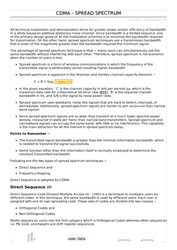
MSP430 FamilyUSART Peripheral InterfaceUSART Peripheral InterfaceThe universal synchronous/asynchronous interface is a serial channel which allows aserial bit stream of 7 or 8 bits to be shifted into and out of the MSP430, at a programmedrate, or at a rate defined by an external clock. The USART peripheral interface is built tosupport, with one hardware configuration, two different serial protocols: the universalasynchronous protocol - often simply called RS232 - and the synchronous serial protocol- usually known as the SPI protocol.The control bit SYNC in control register UCTL is used to select the required mode:SYNC 0:asynchronous - UART - mode selectedSYNC 1:synchronous - SPI - mode selected.The USART is connected to the CPU as a byte peripheral module. It connects thecontroller to the external system environment by three or four external pins.Receive StatusReceive Buffer URXBUFSYNCRXEMMListen0110SYNCSOMIReceive Shift RegisterSSEL1SSEL0UCLKI0ACLK12MCLKMCLKSYNCSYNCBaud Rate Generator0Baud Rate Register UBRURXDSTE312SYNCBaud Rate Generator13UCLKSUTXDWUT1Transmit ShiftRegisterSIMO0CKPHTXWakeTransmit Buffer UTXBUFSYNCCKPLUCLKIUCLKClock Phase & PolarityUCLKSFigure 12.1: Block diagram of USART12-III
USART Peripheral Interface121312-IVMSP430 Family
MSP430 Family12USART Peripheral Interface, UART ModeUSART Peripheral Interface, UART ModeThe universal synchronous/asynchronous interface is a serial channel which allows aserial bit stream of 7 or 8 bits to be shifted into and out of the MSP430 at a programmedrate. The asynchronous mode is selected when the control bit SYNC in the USARTcontrol register UCTL is reset. The USART is connected to the CPU as a byteperipheral. It connects the controller to the external system environment by threeexternal pins.USART’s serial asynchronous communication feature: Asynchronous modes, including Idle line/Address bit communication protocolsTwo shift registers shift serial data stream into URXD, and out on UTXDData transmitted/received with LSB firstProgrammable transmit and receive bit rateStatus flagsSYNC 0Receive StatusReceive Buffer URXBUFRXEListen0Receive Shift Register1SSEL1SSEL0UCLKI0ACLK12MCLKMCLKBaud Rate GeneratorURXDUCLKS12Baud Rate Register UBR3Baud Rate GeneratorWUTTransmit ShiftRegisterLSB firstUTXDCKPLTXWakeTransmit Buffer UTXBUFUCLKIUCLKClock PolarityUCLKSFigure 12.1: Block diagram of USART - UART mode12-1
USART Peripheral Interface, UART ModeMSP430 Family12.1 Asynchronous OperationIn the asynchronous mode, the receiver synchronizes itself to frames, but the externaltransmitting and receiving devices do not use the same clock source; the baud rate isgenerated locally.12.1.1 Asynchronous Frame FormatThe asynchronous frame format consists of a start bit, seven or eight data bits,even/odd/no parity bit, an address bit in Address bit mode, and one or two stop bits. Thebit period is defined by the selected clock source and the data in the baud rate registers.ST D0.MarkD6 D7 AD PA SP SPSpace[2nd stop bit, SP 1][Parity bit, PENA 1][Address bit, MM 1][8th data bit, CHAR 1][optional bit, condition]Figure 12.2: Asynchronous frame format12The receive (RX) operation is initiated by the receipt of a valid start bit. It consists of anegative edge at URXD, followed by the taking of a majority vote from three samples,where 2 of the samples must be zero. These samples occur at n/2-x, n/2 and n/2 x ofBRCLK periods after the negative edge. This sequence provides false start bit rejection,and also locates the center of bits in the frame, where the bits will be read on a majoritybasis. The timing of x is 1/32 to 1/63 times of BRCLK, but at least BRCLK, depending onthe division rate of the baud rate generator.Falling edgeon URXDindicates startbitBRCLKHLUTXDHLURXDHL1Majority votetaken fromURXD data line23n/2-xn/2n/2 xn-1n1n-1nn 1Data bit period n or n 1 BRCLK periodsData bit period n or n 1 BRCLK periodsFigure 12.3: Asynchronous bit format. Example for n or n 1 clock periods12-22312
MSP430 FamilyUSART Peripheral Interface, UART Mode12.1.2 Baud rate generation in asynchronous communication formatThe baud rate generation in the MSP430 differs from other standard serialcommunication interface implementations.Standard Baud Rate GenerationThe standard implementation uses a prescaler from any clock source and a fixedsecond clock divider which is usually a divide by 16.07 07UBR0Select Clock source8Clock1::ClocknStartBRCLKStartUBR115816bit Prescaler / Divider: 31415161Take majority vote of receive bitFigure 12.4: Standard baudrate generation - other than MSP430Baudrate Error!Using this common scheme to generate the baud rate can not generate baud rates thatare chosen close to the frequency of the prescaler’s input frequency BRCLK. Divisionfactors of e.g. 18 are not possible, as well as non-integer factors - for example 13.67.Example 1Assuming a clock frequency of 32,768Hz for the BRCLK signal, and a required baudrateof 4800 Baud, the division factor is 6.83. In a standard baud rate generator the minimumfactor is 16 - the crystal’s frequency and the baud rate generation can not meet therequirements.Example 2Assuming a clock frequency of 1.04MHz (32 x 32,768Hz) for BRCLK signal and arequired baudrate of 19 200 Baud, the division factor is 54.61. In a standard baud rategenerator the next factors are 48 (3x16) or 64 (4x16) - the crystal’s frequency and thebaud rate generation can not meet the requirements. The crystal frequency needs to beselected to meet the communication requirements. Other criteria like currentconsumption, simple real-time clock function or system cost constraints can not beconsidered to be favorable.12-312
USART Peripheral Interface, UART ModeMSP430 FamilyMSP430 Baud Rate GenerationThe baud rate generator of the MSP430 uses one prescaler/divider and a modulator.This combination is used to work properly with crystals whose frequency is not a multipleof the standard baud rates, but allows the protocol to run at maximum baud rate. Usingthis technique, even with a watch crystal (32,768Hz) baudrates up to 4800 (9600) baudare possible. This gives power advantages, since the selection of sophisticated MSP430operation in low power mode is K7 0UBR0BRCLK381515bit Prescaler / DividerQ1 . Q15ToggleFFCompare 0 or 1mBITCLKShift Modulation Register Datashift outshift in07Modulation Register UMOD12StartHLBRCLKHLCounterBITCLKn/2 n/2-1 n/2-21110n/2 n/2-1n/2n/2n/2-1 n/2-2n/2-1 n/2-2211100n/2n/2 n/2-1n/2 n/2-1 n/2-2HLDivide byINT(n/2), m 0INT(n/2) m( 1)n(even), m 0n (odd) or n(even) m( 1)n(odd) m( 1)Figure 12.5: MSP430 Baud Rate Generation. Example for n or n 1 clock periodsThe LSB of the modulation register is used first for modulation - it starts with the start bit.A set modulation bit increases the division factor by one.Example 1Assuming a clock frequency of 32,768Hz for BRCLK signal and a required baudrate of4800 Baud, the division factor is 6.83. The baud rate generation in the MSP430’sUSART uses a factor of 6 plus the modulation register loaded with 6Fh (0110 1111).This means the divider runs the following sequence: 7 - 7 - 7 - 7 - 6 - 7 - 7 -6 - .The sequence repeats after all eight bits of the modulator are used.12-4
MSP430 FamilyUSART Peripheral Interface, UART ModeExample 2Assuming a clock frequency of 1.04MHz (32 x 32,768Hz) for BRCLK signal, and arequired baudrate of 19 200 Baud, the division factor is 54.61 The baud rate generationin the MSP430’s USART uses a factor of 54 (36h) plus the modulation register loadedwith 0D5h. This means the divider runs the following sequence: 55 - 54 - 55 - 54 - 55 54 - 55 -55 - . The sequence repeats after all eight bits of the modulator are used.The standard baud rate data needed for the baud rate registers and the modulationregister are listed for the watch crystal 32,768Hz (ACLK) and MCLK, assumed to be32 times the ACLK frequency. The error listed is calculated for the receive path. Inaddition to this error, the synchronization error should also be considered.ACLKDivide byBaud ratemax.errorMCLK ( 32 x ACLK) max.errorUBR1 UBR0 .230034A-21/1206D03-.4/1UBR1UBR0 UMOD%19 20054.610366B-.2/238 40027.3101B03-4/376 80013.6500D6B-6/3115 2009.1000908-5/7Table 12.1: Commonly used Baud Rates, Baudrate data and errorsCommonlyThe maximum error is calculated for the receive mode and the transmit mode. The errorin the receive mode is the accumulating timing error versus the ideal scanning time inthe middle of each bit. The transmit error is the accumulating timing error versus theideal time of the bit period.The maximum frequency of MCLK is noted in the device data sheet and can exceed theexample frequency.12-512
USART Peripheral Interface, UART ModeMSP430 Family12.1.3 Asynchronous Communication FormatsThe USART module supports two multiprocessor communication modes when theasynchronous mode is used. These formats can be used to transfer informationbetween many microcomputers on the same serial link. Information is transferred as ablock of frames from a particular source to one or more destinations. The USART hasfeatures to identify the start of blocks, and to suppress interrupts and status informationfrom the receiver, until a block start is identified. In both multiprocessor modes, thesequence of data exchange with the USART module could be based on polling of data,or using the receive interrupt features.Both asynchronous multiprocessor protocols, the idle line and the address bitmultiprocessor mode allow efficient data transfer between multiple communicationsystems. They also can be used to minimize activity of the system, whether to savecurrent consumption or processing resources. The MM bit in the control register definesthe address bit or idle line multiprocessor protocol mode. Both formats use the wake upon transmitting, using the address feature function (TXWake bit), and on activating theRXWake bit. The URXWIE and URXIE bits control the transmit and receive features ofthese modes.12.1.4 Idle line multiprocessor modeIn this mode, blocks of data are separated by an idle time between them. An idle receiveline is detected when 10 or more 1s in a row are received after the first stop bit of acharacter.Blocks of frames12UTXD/ HURXD LIdle periods of 10 bits or moreUTXD/URXD EXPANDEDUTXD/ HURXD LSTADDRESSSP STFirst frame within block isaddress. It follows idleperiod of 10 bits or more.Figure 12.6: Idle line multiprocessor protocol12-6DATASPSTDATASPFrame within blockFrame within blockIdle periodless than10 bits
MSP430 FamilyUSART Peripheral Interface, UART ModeWhen two stop bits are used, the second one is counted as the first 'Mark' bit of the idleperiod. The first character received after an idle period is an address character. TheRXWake bit can be used as an address tag for the character. In idle line multiprocessorformat, RXWake bit is set when a received character is an address character and istransferred into the receive buffer.Example:one stopbit10 bit idle periodMarkXXXXX SPST XXXXXXXSpaceExample:two stopbitMark10 bit idle periodXXXXX SP SPST XXXXXXXSpaceSP: stopbitST: startbitFigure 12.7: USART Receiver Idle DetectNormally, if the USART’s URXWIE bit in the receive control register is set, characterswill be assembled as usual by the receiver, but they will not be transferred to thereceiver buffer, URXBUF, nor will interrupts be generated. When an address characteris received, the receiver is temporarily activated to transfer the character to URXBUFand set the URXIFG interrupt flag. Appropriate error status flags will be set. Theapplication software can validate the received address. If there is a match, theapplication software will handle the further data processing and execute properoperation. If not, the processor waits for the next address character to arrive. TheURXWIE bit itself is not modified by the USART: it should be modified by the user inorder to receive non-address characters or address characters.In idle line multiprocessor mode, a precise idle period can be generated to createefficient address character identifiers. Associated with the TXWake bit is the wake-uptemporary (WUT) flag. WUT is an internal flag, double buffered with TXWake. When thetransmitter is loaded from UTXBUF, WUT is loaded from TXWake, and TXWake bit isreset.TXWakeTX Buffer UTXBUFWUTTX Shift RegisterStart bitParity bitTX signalFigure 12.8: Double-Buffered WUT and TX Shift Register12-712
USART Peripheral Interface, UART ModeMSP430 FamilySending out an idle frame to identify an address character is accomplished as follows:The TXWake bit should be set, and then any word (don't care) must be written to theUTXBUF (UTXIFG should be set). When the transmitter shift register is empty (TXEPTis set), the contents of the UTXBUF are shifted to the transmit shift register, and theTXWake value is shifted to WUT. When the WUT bit has been set, the start, data, andparity bits will be suppressed and an idle period of exactly 11 bits will be transmitted.The next data word, shifted out of the serial port after the address character identifyingidle period, will be the second word written to the UTXBUF after TXWake bit was set.The first data word written is suppressed while the address identifier is sent out, andignored after that. Writing the first don't care word to UTXBUF is necessary so that theTXWake bit value can be shifted to WUT.Example: one stopbit11 bit idle periodMarkXXXXX SPST XXXXXXXSpaceExample: two stopbitsMark11 bit idle periodXXXXX SP SPSpaceSP: stopbitST: startbitFigure 12.9: USART Transmitter Idle Generation1212-8ST XXXXXXX
MSP430 FamilyUSART Peripheral Interface, UART Mode12.1.5 Address bit FormatIn this mode, characters contain an extra bit that is used as an address indicator. Thefirst character in a block of data carries an address bit that is set to indicate that thecharacter is an address. The RXWake bit is set when a received character is an addresscharacter, and is transferred into the receive buffer (receive conditions are true).Normally, if the USART’s URXWIE bit is set, data characters will be assembled as usualby the receiver, but they will not be transferred to the receiver buffer URXBUF nor willinterrupts be generated. When a character is received that has an address bit set, thereceiver is temporarily activated to transfer the character to URXBUF and set theURXIFG. Error status flags will be set as appropriate. The application SW handles thesucceeding operation for the best benefit in processing resource handling or currentconsumption reduction. The application software can validate the received address. Ifthere is a match, the processor can read the remainder of the data block. If not, theprocessor waits for the next address character to arrive.Blocks of framesUTXD/URXDHLIdle periods of no significanceTXD/RXD EXPANDEDUTXD/URXDHLSTADDRESS1 SP STFirst frame within block is anaddress.The ADDR/DATAbit is "1".DATA0 SPSTDATA0 SPADDR/DATA bit is "0"for data within block.Idle time is ofno significanceFigure 12.10: Address bit multiprocessor protocolIn address bit multiprocessor mode, the address bit of a character can be controlled bywriting to the TXWake bit. The value of the TXWake bit is loaded into the address bit ofthat character each time a character is transferred from the transmit buffer UTXBUF tothe transmitter. The TXWake bit is then cleared by the USART.12-912
USART Peripheral Interface, UART ModeMSP430 Family12.2 Interrupt and Control FunctionThe USART peripheral serves two main interrupt sources, for transmission andreception. Two individual interrupt vectors are available, one for receive and one fortransmit interrupt events.The control bits of the USART are located in the SFR address range: Receive Interrupt FlagReceive Interrupt EnableReceive EnableTransmit Interrupt FlagTransmit Interrupt EnableTransmit EnableURXIFGURXIEURXEUTXIFGUTXIEUTXEinitial state reset (by PUC/SWRST)initial state reset (by PUC/SWRST)initial state reset (by PUC)initial state set (by PUC/SWRST)initial state reset (by PUC/SWRST)initial state reset (by PUC)The receiver and transmitter of the USART operate fully independently, but use thesame baud rate generator. Transmit and receive use the same baud rate.12.2.1 USART Receive EnableThe Receiver Enable bit URXE enables or disables the receiver from collecting the bitstream on the URXD data line. Disabling the USART receiver will stop the receiveoperation after completing a receive operation which has been started, or stopimmediately if no receive operation is active. The start bit detection is disabled.No valid start bitnot completedURXE 012ReceivedisableURXE 1URXE 0Idle State(Receiverenabled)URXE 1,valid start bitReceivercollectsCharacterHandle InterruptConditionscharacterreceivedURXE 1URXE 0Figure 12.11: State diagram on Receiver enable URXENote:URXE re-enable, UART ModeSince the receiver is completely disabled a re-enable of the receiver isasynchronous to any data stream on the communication line. Synchronizationcan be done by looking for an idle line condition before accepting any receivedcharacter.12-10
MSP430 FamilyUSART Peripheral Interface, UART Mode12.2.2 USART Transmit EnableThe transmit enable bit UTXE enables or disables a character transmission on the serialdata line. If this bit is reset, the transmitter is disabled but any active transmission is nothalted until all data previously written into the transmit buffer has been sent. If thetransmission is completed, any further write to the transmitter buffer will not result in adata transmission.UTXE 0TransmitdisableUTXE 1UTXE 0no data writtento transmit bufferIdle State(Transmitterenabled)UTXE 1,data written totransmit buffernot completedTransmissionactiveHandle InterruptConditionscharactertransmittedUTXE 1UTXE 0Figure 12.12: State diagram on Transmitter enableWhen UTXE is reset any data can be written regularly into the transmit buffer, but notransmission is started. Once the UTXE bit is set, an immediate start of transmission ofthe character presently in the buffer is initiated. This character is transmitted correctly.Note:Write to UTXBUF, UART Mode12Data should never be written into the transmit buffer UTXBUF when it is notready and the transmitter is enabled (UTXE is set). If it is, the character shiftedout can be random.12-11
USART Peripheral Interface, UART ModeMSP430 Family12.2.3 USART Receive Interrupt OperationThe receive interrupt flag URXIFG is set or is unchanged each time a character isreceived and loaded into the receive buffer: Erroneous characters (parity, frame or break error) will not set interrupt flagURXIFG when URXEIE is reset: URXIFG is unchanged. All type of characters (URXWIE 0) or only address characters (URXWIE 1) will setthe interrupt flag URXIFG pending on the bit URXWIE. When URXEIE is also set,erroneous character will set the interrupt flag URXIFG.SYNCValid start bitReceiver collects characterURXSEfrom URXDτPEFEBRKURXSClearURXIEErroneous characterwill not set flag URXIFGURXEIERequest Interrupt ServiceSYNC(S)ClearURXWIERXWakeEach character or addressaddresswill set flag URXIFG12URXIFGcharacter receivedORbreak detectedSWRSTPUCURXBUF readURXSEIRQAFigure 12.13: Receive Interrupt ConditionsURXIFG is reset at system reset PUC, or at a software reset SWRST. URXIFG is resetautomatically if the interrupt is served (URXSE 0) or the receive buffer URXBUF is read.The Receive Interrupt Flag URXIFG indicates, if set, an interrupt event waiting to beserved. The Receive Interrupt Enable bit URXIE enables, if set, serving of a waitinginterrupt request. Both the receive interrupt flag URXIFG and the receive interruptenable bit URXIE are reset with PUC and SWRST.The signal URXIFG can be accessed by software. Signal URXS can not be accessed bysoftware. When both interrupt events - receive start detection and character receiveaction - are enabled by software, the flag URXIFG indicates that a character wasreceived and not the start detect request interrupt service. This works, since the interruptsoftware handler for the receive start detection will reset the URXSE bit. This clears theURXS bit and prevents further interrupt requests from URXS. The URXIFG should bealready reset since no set condition was at this time at URXIFG latch.12-12
MSP430 FamilyUSART Peripheral Interface, UART Mode12.2.4 USART Transmit Interrupt OperationThe transmit interrupt flag UTXIFG is set by the transmitter to indicate that thetransmitter buffer UTXBUF is ready to accept another character. This bit is automaticallyreset if the interrupt request service is started or a character is written into the UTXBUF.This flag will assert a transmitter interrupt if the local (UTXIE) and general (GIE) interruptenable bit are set. The UTXIFG is set after system reset PUC or SWRST are removed.UTXIEQClearPUC or SWRSTSetVCCcharacter moved frombuffer to shift registerDQUTXIFGClearRequest Interrupt ServiceSWRSTUTXBUF written into transmit shift registerIRQAFigure 12.14: Transmit Interrupt ConditionThe transmit interrupt enable UTXIE bit controls the ability of the UTXIFG to request aninterrupt but does not prevent the flag UTXIFG from being set. The UTXIE is reset withPUC or software reset bit SWRST. The UTXIFG bit is set after system reset PUC orsoftware reset SWRST, but the UTXIE bit is reset to ensure full interrupt controlcapability.1212-13
USART Peripheral Interface, UART ModeMSP430 Family12.3 Control and Status RegisterThe USART module hardware is byte structured and should be accessed by byteprocessing instructions (suffix 'B'). Registershort form Register typeUSART Control registerTransmit Control registerReceive Control registerModulation Control reg.Baud Rate register 0Baud Rate register 1Receive BufferTransmit ss Initial stateType of read/writeType of read/writeType of read/writeType of read/writeType of read/writeType of read/writeType of read/writeType of read070h071h072h073h074h075h076h077hSee .individual .bit hangedAll bits are random after PUC, unless noted otherwise by the detailed functionaldescription.Reset of the USART is performed by PUC or SWRST bit. After power-up clear (PUC)the SWRST bit remains set and the USART remains in this condition until the reset isdisabled by resetting the SWRST bit.The USART module operates in asynchronous or in synchronous mode defined by theSYNC bit. The bits in the control registers may have different functions in the twomodes. All bits in this section are described with their functions in the asynchronousmode - SYNC 0. Their functions in the synchronous mode are described in theUSART’s serial peripheral interface section.12.3.1 USART Control register UCTL12The information stored in the control register determines the basic operation of theUSART module. The register bits select the communications protocol, communicationmode and parity bit. All bits should be programmed according to the selected modebefore reset is disabled by resetting bit nrw-0SYNCrw-0MMrw-0SWRSTrw-1Figure 12.15: USART Control Register UCTLBit 0:12-14The USART state machines and operating flags are initialized to the resetcondition if the software reset bit is set. Until the SWRST bit is reset, allaffected logic is held in the reset state. This implies that after a system resetthe USART must be re-enabled by resetting this bit. The receive andtransmit enable flags URXE and UTXE are not altered by SWRST.
MSP430 FamilyBit 1:Bit 2:Bit 3:Bit 4:Bit 5:Bit 6:Bit 7:USART Peripheral Interface, UART ModeMultiprocessor mode (address/idle line wake up).Two multiprocessor protocols, idle line and address bit, are supported by theUSART module. The choice of multiprocessor mode affects the operation ofthe automatic address decoding functions.MM "0" : Idle line multiprocessor protocolMM "1" : Address bit multiprocessor protocolThe conventional asynchronous protocol uses MM bit resetMode or function of USART module selected.The SYNC bit selects the function of the USART peripheral interfacemodule. Some of the USART control bits will have different functions inUART and SPI mode.SYNC 0 : UART function is selected.SYNC 1 : SPI function is selected.The Listen bit selects if the transmitted data is fed back internally to thereceiver.Listen 0 : No feed back.Listen 1 : Transmit signal is internally fed back to the receiver. Eachtransmission from the MSP430’s USART is received paralleland no external signal is received anymore.Character length.This register bit selects the length of the character to be transmitted as 7 or8 bits. Characters of 7 bits do not use the eighth bit in URXBUF andUTXBUF and this bit is padded with "0".CHAR 0 : 7 bit data.CHAR 1 : 8 bit data.Number of stop bits.This bit determines the number of stop bits transmitted. The receiver checksfor one stop bit only.SP 0 : one stop bit.SP 1 : two stop bits.Parity odd/even.If PENA bit is set (parity bit is enabled), the PEV bit defines odd or evenparity according to the number of odd or even "1" bits in both transmittedand received characters, address bit (address bit multiprocessor mode) andparity bit.PEV 0 : Odd parityPEV 1 : Even parity.Parity enable.If parity is disabled no parity bit is generated during transmission orexpected during reception. A received parity bit is not transferred to theURXBUF with the received data as it is not considered as one of the databits. During address bit multiprocessor mode, the address bit is included inthe parity calculation.PEN 0 : Parity disablePEN 1 : Parity enable12-1512
USART Peripheral Interface, UART ModeNote:MSP430 FamilyMARK, SPACE definitionThe MARK condition is identically to the signal level in the idle state. SPACE isthe opposite signal level: the start bit is always SPACE.12.3.2 Transmit Control Register UTCTLThe register UTCTL controls the USART hardware associated with transmit operation.70UTCTL071hunused CKPLrw-0rw-0SSEL1 SSEL0 URXSE TXWake unused TXEPTrw-0rw-0rw-0rw-0rw-0rw-1Figure 12.16: USART Transmitter Control RegisterBit 0:Bit 1:Bit 2:Bit 3:12Bit 4,5:Bit 6:Bit 7:12-16The transmitter empty TXEPT flag is set when the transmitter shift registerand UTXBUF are empty, and reset when data is written to UTXBUF. It is seton SWRST.unusedThe TXWake bit is used to control the transmit features of themultiprocessor communication modes. Each transmission - started byloading the UTXBUF - uses the state of the TXWake bit to initialize thefeature of address identification. It should not be cleared - the USARThardware clears this bit once it has been transferred to "Wake UpTemporary", WUT; SWRST also clears TXWake bit.The receive start edge control bit requests - if set - a receive interruptservice. For a successful interrupt service the corresponding enable bitsURXIE and GIE should be set. The advantage of this bit is to start thecontroller’s clock system including MCLK along with the interrupt service,and keep it running by modifying the mode control bits. The USART isworking with selected MCLK properly, even if the system is switched to alow power mode with disabled MCLK.Source Select 0 and 1.The source select bit defines which clock source is used for the baud rategeneration:SSEL1,SSEL00external clock selected, UCLKI1auxiliary clock selected, ACLK2, 3main system clock selected, MCLKClock polarity CKPL.The CKPL bit controls the polarity of the UCLKI signal.CKPL 0:the UCLKI signal has same polarity than UCLK signal.CKPL 1:the UCLKI signal has inverted polarity of UCLK signal.Unused
MSP430 FamilyUSART Peripheral Interface, UART Mode12.3.3 Receive Control Register URCTLThe register URCTL controls the USART hardware associated with the receiveroperation and holds error and wakeup conditions modified by the latest character writtento the receive buffer URXBUF. Once any of the bits FE, PE, OE, BRK, RXERR orRXWake is set, they are not reset by receiving another character. They are reset byaccessing the receive buffer URXBUF, by a USART SW reset SWRST, a system resetPUC or by XEIE URXWIERXWake RXERRrw-0rw-0rw-0rw-0Figure 12.17: USART Receiver Control R
The control bit SYNC in control register UCTL is used to select the required mode: SYNC 0: asynchronous - UART - mode selected SYNC 1: synchronous - SPI - mode selected. The USART is connected to the CPU as a byte peripheral module. It connects the controller to the external system environment by three or four external pins. Receive Buffer .