Transcription
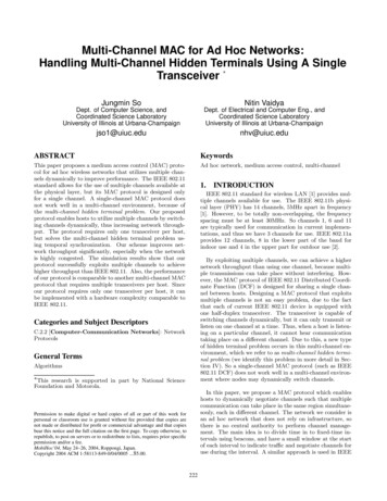
IEEE JOURNAL OF SELECTED TOPICS IN QUANTUM ELECTRONICS, VOL. 27, NO. 3, MAY/JUNE 20213400108Design of Hybrid Plasmonic Multi-Quantum-WellElectro-Reflective Modulators Towards 100 fJ/bitPhotonic LinksXiaoxin Wang, Shaoliang Yu , Haijie Zuo, Xiaochen Sun, Member, IEEE, Juejun Hu, Member, IEEE,Tian Gu , Member, IEEE, and Jifeng Liu , Senior Member, IEEEAbstract—Realization of on-board and inter-chip optical interconnects requires a photonic data link with power consumptionwell below their electrical counterparts (i.e., 1 pJ/bit). Currently, directly modulating 850 nm vertical cavity surface emittinglasers at 50 Gb/s requires 2–4 pJ/bit/channel. External reversebiased modulators could drastically reduce this power consumption. Here we design ultralow power GaAs/AlGaAs multi quantumwell electro-reflective modulators operating at 1 V for facile integration with polymer “optical bridges”, utilizing coupled quantumconfined Stark effect between adjacent quantum wells and opticalcoupling to hybrid surface plasmon-slab modes for significantlyenhanced extinction ratio and spectral bandwidth. Distinctive fromconventional electro-optical or electro-absorption modulators, thisnew design synergistically leverages ultra-large changes in bothrefractive index ( Δn 0.05) and absorption coefficient (Δα 104cm 1 ), achieving 35-50 dB extinction ratio at 1 V reverse biaswith a low insertion loss of 1–3 dB, an incident angle toleranceof 5 , and a spectral bandwidth of 7–10 nm. The modulatorpower consumption is 1.9 fJ/bit without the need of thermaltuning, and the RC-limited bandwidth well exceeds 100 GHz.This new modulator enables high bandwidth and ultralow poweroptical interconnect networks at 100 Gb/s/channel and 100fJ/bit/channel compatible with ever-scaling CMOS technologies.Index Terms—Electromagnetic propagation in plasma media,optical interconnections, optical modulation, optical surface waves,quantum confined stark effect, quantum well devices.I. INTRODUCTIONPTICAL interconnects (OI) have been playing anincreasingly important role in large-scale data centersand high-performance computing systems for rack-to-rack andboard-to-board communication to address the rapidly growingOManuscript received December 19, 2019; revised March 18, 2020; acceptedMarch 31, 2020. Date of publication April 20, 2020; date of current versionJune 22, 2020. This work was supported by the U.S. Department of Energythrough ARPA-E ENLITENED Program under the award #DE-AR0000847.(Corresponding author: Jifeng Liu.)Xiaoxin Wang and Jifeng Liu are with Dartmouth College, Thayer Schoolof Engineering, Hanover, NH 03755-4401 USA (e-mail: Xiaoxin.Wang@dartmouth.edu; Jifeng.Liu@dartmouth.edu).Shaoliang Yu, Haijie Zuo, Juejun Hu, and Tian Gu are with the MassachusettsInstitute of Technology, Department of Materials Science and Engineering,Cambridge, MA 02139-4307 USA (e-mail: yusl@mit.edu; hzuo@mit.edu;hujuejun@mit.edu; gutian@mit.edu).Xiaochen Sun is with LaXense, Inc., West Covina, CA 91790 USA (e-mail:sun@laxense.com).Color versions of one or more of the figures in this article are available onlineat https://ieeexplore.ieee.org.Digital Object Identifier 10.1109/JSTQE.2020.2987174Fig. 1. (a) Schematics of a chip-to-chip SHINE layout co-packaged withintegrated circuit chips showing the integration of VCSEL, MQW modulator andphotodetector (PD) with polymer waveguide optical bridges. (b) The modulationprinciple of the hybrid plasmonic MQW (HP-MQW) modulator is schematicallyillustrated for “ON” state (0 V) and “OFF” state with a low applied voltage 1 V. In the “ON” state the incident light from the input waveguide is mostlyreflected by a 20 nm Au thin film to the output waveguide. In the “OFF”state, the incident light is coupled to a hybrid plasmonic-MQW slab mode toachieve a high extinction ratio. (c) A more detailed schematic cross-section of theHP-MQW modulator structure. (d) FDTD simulation of the coupling betweenthe polymer waveguides (TM polarization) and the HP-MQW modulator region,demonstrating a low coupling loss of 0.5 dB. The inset on the left shows theprofile of the focal spot projected on the surface of the HP-MQW modulator.The inset on the right shows the mode profile of the output waveguide.demand for higher energy-efficiency and bandwidth. The implementation of on-board OI at chip-to-chip and chip-to-memorylevel will ultimately fulfill an all-optical interconnect withlink power consumption well below state-of-the-art electricalinterconnects ( 1 pJ/bit) [1]. However, no mature technicalpathways have yet been available for inter-chip OI. Onecandidate technology is Si photonics (SiP), which are fabricatedusing CMOS processes to interconnect electronic chips throughmulti-level integration [1], [2]. However, high density opticalI/O packaging and chip-to-chip coupling remains a significantchallenge. Recently, we proposed a Seamless Hybrid-integratedInterconnect Network (SHINE) architecture (Fig. 1(a)) [3], inwhich an “optical bridge” platform comprising flexible polymerribbon waveguide arrays integrated with III-V active devicesis employed for OIs between Si-CMOS chips co-packaged1077-260X 2020 IEEE. Personal use is permitted, but republication/redistribution requires IEEE permission.See l for more information.Authorized licensed use limited to: MIT Libraries. Downloaded on October 13,2020 at 04:13:41 UTC from IEEE Xplore. Restrictions apply.
3400108IEEE JOURNAL OF SELECTED TOPICS IN QUANTUM ELECTRONICS, VOL. 27, NO. 3, MAY/JUNE 2021with the optical components. Instead of utilizing planarwaveguide integration of photonic components in SiP, theoptical bridge integrates compact and efficient surface-incidentactive photonic components with single mode flexible polymerwaveguides via freeform optical couplers [3]. This uniquecombination enables high bandwidth density, low optical lossesand low-cost packaging compatible with standard flip-chip andhigh-throughput pick-and-place technologies.The active photonic components in the optical bridge includecontinuous-wave single-mode vertical-cavity-surface-emittinglasers (VCSELs), modulators and detectors (PDs). Nowadays,directly modulated VCSELs emitting at 850 nm dominate shortreach communications ( 300 m) in data centers. However, thebandwidth of direct modulation is approaching the limit set bythe internal carrier dynamics ( 30 GHz or 56 Gb/s) [4]–[6].The laser driver for 50 Gb/s direct modulation also consumesa large amount of power on the order of pJ/bit due to thenecessity of ultrafast, high-level carrier injection [7], leadingto an energy consumption on the order of several pJ/bit/channel[6]. Therefore, we adopt reverse biased external modulators inthe SHINE architecture to significantly reduce the power consumption. In contrast to high speed laser drivers, state-of-the-artdrivers for reserve biased modulators is 1.2 C Vpp 2 , where Cis the capacitance of the modulator and Vpp is the peak-to-peakvoltage swing [8]. With compact micro/nanophotonic modulatorstructures, the modulator driver only consumes 10–100 fJ/bit,i.e., one to two orders of magnitude more energy efficient thanthe high-speed lasers drivers. The external modulator is requiredto simultaneously meet the challenges of high bandwidth, largeextinction ratio (ER), low insertion loss (IL), low driving voltage,and reasonably broad operation spectral range to circumvent theneed for active thermal stabilization.For facile coupling with VCSELs, surface-incident modulators are preferred for the SHINE architecture. Conventionally,electro-optical modulators (EOMs) and electro-absorption modulators (EAMs) are the two types of devices used for externalmodulation. They utilize the change in the real part (Δn) andimaginary part (Δk) of the refractive index under an appliedvoltage, respectively. EOMs usually require a waveguide and/orresonator structure for a sufficiently long light-matter interactionlength to implement π phase shift since Δn is usually limited to10 4 –10 3 . They are seldom used in surface incident configuration. Recent advances in integrated photonics have demonstratedthat EAMs are very promising to achieve ultralow power modulation at high bandwidth. These devices utilize Franz-Keldysheffect (FKE) in bulk semiconductors and quantum-confinedStark effect (QCSE) in multiple quantum well (MQWs) [2], [9].Waveguide-integrated Ge/GeSi [10], [11] and hybrid III-V-on-SiEAMs [12] have presented a modulation bandwidth of 50-74GHz and an extinction ratio (ER) of 5-10 dB at 2-4 V drivingvoltage in the wavelength range of λ 1.5 1.6 μm and 1.3 μm,respectively, at a power consumption of 10-100 fJ/bit. Previousresearch has also demonstrated high-density, high-yield hybridintegration of surface incident GaAs/Alx Ga1-x As MQW EAMson Si CMOS via flip-chip solder-bonding [13]. However, thesedevices usually require a high driving voltage of 7–10 V toachieve an adequate ER due to the limited MQW thickness, evenwhen embedded in a resonant Fabry-Pérot (FP) cavity to acquiremultiple-pass absorption based on QCSE [13]–[20]. These highdriving voltages are not compatible with the current CMOStechnology nodes. By comparison, the recent demonstrationof polymer waveguide-coupled surface-normal reflective EAMswith ER 4 dB at a bias voltage of 4 V proves their capabilityof full integration within a single photonic layer for chip-levelOIs, although the driving voltage should be further reduced andER further enhanced [21].In this paper, we design ultralow power hybrid plasmonicMQW (HP-MQW) GaAs/AlGaAs electro-reflective modulatorsoperating at 1 V for facile integration with waveguide interconnects exemplified by SHINE. Distinctive from conventionalEOM and EAMs, this new design synergistically leveragesultra-large changes in both the refractive index ( Δn 0.05)and absorption coefficient (Δα 104 cm 1 ), thereby efficientlycoupling the incident light into hybrid plasmonic slab modesunder 1 V reverse bias for an ER 30 dB at a low IL of1–3 dB. The coupled QCSE (Co-QCSE) between adjacent QWsincreases the spectral bandwidth to 7–9 nm, significantly broaderthan micro-resonator-based modulators ( 0.1 nm) [22]–[23] ata similar footprint (3–5 μm in diameter) and capacitance ( 1fF) to allow even lower power consumption by avoiding activethermal tuning. This high-performance modulation and high efficiency coupling with polymer waveguides enables an ultralowtotal power consumption of 100 fJ/bit/link in the SHINE network. The same device structure and coupling scheme are alsoapplicable to surface-incident PDs in the SHINE architecture,thereby further facilitating photonic integration.II. PRINCIPLES OF HIGH-PERFORMANCE HP-MQWELECTRO-REFLECTIVE MODULATORSIt has been well known that the absorption change Δαdue to QCSE in GaAs/Alx Ga1-x As MQW can be as large as5000-10000 cm 1 under an electric field of 70 kV/cm [24].Accordingly, the refractive index change Δn reaches as much as 0.05 near 850 nm wavelength, as deduced by Kramers-Kronigrelation [25] and first experimentally verified by Glick et al[26]. Note that this huge Δn ( 0.05) is two to three orders ofmagnitude higher than those in LiNbO3 and Si EOMs. However,conventionally such a large Δn near the direct bandgap ofGaAs QWs cannot be directly applied to EOMs due to thelarge absorption near the direct gap, which leads to a hugeIL. Considering that surface plasmon resonance (SPR) is verysensitive to the refractive index of the dielectric material nearby,we adopt a new approach by coupling the incident light intoa hybrid plasmonic-MQW slab mode in the OFF-state at areverse bias, thereby drastically reducing the driving voltage andincreasing the ER (see Fig. 1(b)). Such coupling synergisticallyutilizes the large Δn and Δα from Co-QCSE. On the other hand,at ON-state (i.e., 0 V) there is almost no coupling to the hybridplasmonic mode, and the modulator structure exhibits a highreflection with minimal IL.A more detailed schematic cross-section of the proposedHP-MQW electro-reflective modulator structure is shown inFig. 1(c). The device comprises a p-i-n diode with an intrinsicGaAs (10 nm)/Al0.3 Ga0.7 As (3.5 nm) MQW region. The thin AlGaAs barrier enables quantum state coupling between adjacentAuthorized licensed use limited to: MIT Libraries. Downloaded on October 13,2020 at 04:13:41 UTC from IEEE Xplore. Restrictions apply.
WANG et al.: DESIGN OF HYBRID PLASMONIC MULTI-QUANTUM-WELL ELECTRO-REFLECTIVE MODULATORS TOWARDS 100 FJ/BITQWs to benefit from Co-QCSE for broader spectral bandwidthand higher ER. A low index dielectric layer, such as CYTOP(n 1.34) [27] or SiO2 (n 1.46), is sandwiched between athin Au layer (20 nm thick) and the p-i-n diode structure. Infact, a hybrid mode between the Au/dielectric surface plasmonand the MQW slab can be supported as long as the refractiveindex of the dielectric layer is lower than the polymer claddinglayer (n 1.51) sitting on top of the Au film. The free-formmicro-optical coupler [3], [28], [29], which can be fabricatedby the two-photon polymerization process with high accuracy,is a critical element to couple the light from the single-modeflexible polymer waveguide to surface-incident modulators andPDs with well-controlled beam properties, such as angle ofincidence, divergence angle, focal spot size, mode profile, etc. Asshown in Fig. 1(d), 3D finite-difference-time-domain (FDTD)simulation indicates that the free-form facets based on totalinternal reflection provide a high coupling efficiency of 90%(or coupling loss 0.5 dB) for TM polarization from the inputwaveguide to the modulator then to the output waveguide overhalf an octave around the targeted wavelength [29]. The incidentlight on the surface of the MQW is p-polarized (i.e., electric fieldparallel to the plane of incidence), enabling surface plasmonexcitation and facilitating optimal coupling conditions requiredby the HP-MQW modulators. This coupling loss is added tothe tot
WANG et al.: DESIGN OF HYBRID PLASMONIC MULTI-QUANTUM-WELL ELECTRO-REFLECTIVE MODULATORS TOWARDS 100 FJ/BIT 3400108 QWs to benefit from Co-QCSE for broader spectral bandwidth and higher ER. A low index dielectric layer, such as CYTOP (n 1.34) [27] or SiO