Transcription
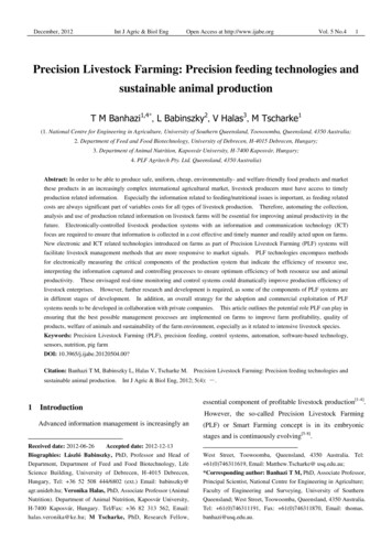
LT1021Precision ReferenceUDESCRIPTIOFEATURES Ultralow Drift: 5ppm/ C Max SlopeVery Low Noise: 1ppm P-P (0.1Hz to 10Hz)100% Noise TestedPin Compatible with Most Bandgap ReferenceApplications, Including Ref 01, Ref 02, LM368,MC1400 and MC1404 with Greatly ImprovedStability, Noise and DriftTrimmed Output VoltageOperates in Series or Shunt ModeOutput Sinks and Sources in Series Mode 100dB Ripple RejectionMinimum Input/Output Differential of 1VAvailable in 5-Lead Can, N8 and S8 PackagesUAPPLICATIO S The LT 1021 is a precision reference with ultralow driftand noise, extremely good long term stability and almosttotal immunity to input voltage variations. The referenceoutput will both source and sink up to 10mA. Threevoltages are available: 5V, 7V and 10V. The 7V and 10Vunits can be used as shunt regulators (two-terminal zeners)with the same precision characteristics as the threeterminal connection. Special care has been taken to minimize thermal regulation effects and temperatureinduced hysteresis.The LT1021 references are based on a buried zener diodestructure that eliminates noise and stability problemsassociated with surface breakdown devices. Further, asubsurface zener exhibits better temperature drift andtime stability than even the best bandgap references.Unique circuit design makes the LT1021 the first ICreference to offer ultralow drift without the use of highpower on-chip heaters.A/D and D/A ConvertersPrecision RegulatorsDigital VoltmetersInertial Navigation SystemsPrecision ScalesPortable Reference StandardThe LT1021-7 uses no resistive divider to set outputvoltage, and therefore exhibits the best long term stabilityand temperature hysteresis. The LT1021-5 and LT102110 are intended for systems requiring a precise 5V or 10Vreference with an initial tolerance as low as 0.05%., LTC and LT are registered trademarks of Linear Technology Corporation.All other trademarks are the property of their respective owners.UTYPICAL APPLICATIOTypical Distribution of Temperature Drift24Basic Positive and Negative Connections21VININOUTVOUTNCLT1021(7 AND 10 ONLY)18IN15OUTGNDGND–VOUT– (V – )VR1 OUTILOAD 1.5mA1296R1–15V(V – )UNITS (%)LT1021DISTRIBUTIONOF THREE RUNS31021 TA01–0– 5 – 4 – 3 – 2 –1 0 1 2 3OUTPUT DRIFT (ppm/ C)451021 TA011021fc1
LT1021W WWAXI UUABSOLUTERATI GS(Note 1)Input Voltage . 40VInput/Output Voltage Differential . 35VOutput-to-Ground Voltage (Shunt Mode Current Limit)LT1021-5 . 10VLT1021-7 . 10VLT1021-10 . 16VTrim Pin-to-Ground VoltagePositive . Equal to VOUTNegative . – 20VOutput Short-Circuit DurationVIN 35V . 10 secVIN 20V . IndefiniteOperating Temperature RangeCommercial . 0 C to 70 CIndustrial . – 40 C to 85 CMilitary . – 55 C to 125 CStorage Temperature Range . – 65 C to 150 CLead Temperature (Soldering, 10 sec). 300 CUWUPACKAGE/ORDER I FOR ATIOTOP VIEWTOP VIEWNC*8NC* 17 NC*6VIN 2NC* 3VOUT5 TRIM**48DNC*VIN 27DNC*DNC* 36V0UTGND 45TRIM**N8 PACKAGE8-LEAD PDIPGNDH PACKAGE8-LEAD TO-5 METAL CAN*CONNECTED INTERNALLY. DO NOT CONNECT EXTERNAL CIRCUITRY TO THESE PINS.**NO TRIM PIN ON LT1021-7. DO NOT CONNECT EXTERNAL CIRCUITRY TO PIN 5 ON LT1021-7TJMAX 150 C, θJA 150 C/W,θJC 45 C/WORDER PART LT1021BMH-10DNC* -10LT1021DMH-10OBSOLETES8 PACKAGE8-LEAD PLASTIC SO*CONNECTED INTERNALLY. DO NOT CONNECT EXTERNAL CIRCUITRY TO THESE PINS.**NO TRIM PIN ON LT1021-7. DO NOT CONNECT EXTERNAL CIRCUITRY TO PIN 5 ON LT1021-7TJMAX 130 C, θJA 130 C/W (N)TJMAX 130 C, θJA 150 C/W (S)N8 ORDER PART N8-10S8 ORDER PART NUMBERLT1021DCS8-5LT1021DCS8-7LT1021DCS8-10S8 PART MARKING210521072110Order Options Tape and Reel: Add #TRLead Free: Add #PBF Lead Free Tape and Reel: Add #TRPBFLead Free Part Marking: http://www.linear.com/leadfree/Consult LTC Marketing for parts specified with wider operating temperature ranges.1021fc2
LT1021ELECTRICAL CHARACTERISTICSThe denotes specifications that apply over the full operating temperaturerange, otherwise specifications are TA 25 C. VIN 10V, IOUT 0, unless otherwise noted.PARAMETERCONDITIONSOutput Voltage (Note 2)LT1021C-5LT1021B-5/LT1021D-5Output Voltage Temperature Coefficient (Note 3)TMIN TJ TMAXLT1021B-5LT1021C-5/LT1021D-5Line Regulation (Note 50023520ppm/ Cppm/ 00150ppm/mAppm/mA0.81.21.5mAmA3.5µVP-PµVRMS 7.2V VIN 10V10V VIN 40V 2 Load Regulation (Sourcing Current)Load Regulation (Sinking Current)0 IOUT 10mA(Note 4) 0 IOUT 10mA(Note 4) Supply Current Output Voltage Noise (Note 6)0.1Hz f 10Hz10Hz f 1kHz3.02.2UNITSVVLong Term Stability of Output Voltage (Note 7) t 1000Hrs Noncumulative15ppmTemperature Hysteresis of Output T 25 C10ppmThe denotes specifications that apply over the full operating temperature range, otherwise specifications are TA 25 C.VIN 12V, IOUT 0, unless otherwise noted.PARAMETERCONDITIONSOutput Voltage (Note 2)Output Voltage Temperature Coefficient (Note 3)Line Regulation (Note 4)TMIN TJ TMAXLT1021B-7LT1021D-7 8.5V VIN 12V12V VIN 40V Load Regulation (Sourcing Current)Load Regulation (Shunt Mode)0 IOUT 10mA(Note 4) 1.2mA ISHUNT 10mA(Notes 4, 5) Supply Current (Series Mode)MINLT1021-7TYPMAXUNITS6.957.007.05V23520ppm/ Cppm/ mA4.0µVP-PµVRMS Minimum Current (Shunt Mode)VIN is Open Output Voltage Noise (Note 6)0.1Hz f 10Hz10Hz f 1kHz4.02.5Long Term Stability of Output Voltage (Note 7) t 1000Hrs Noncumulative7ppmTemperature Hysteresis of Output T 25 C3ppm1021fc3
LT1021ELECTRICAL CHARACTERISTICSThe denotes specifications that apply over the full operating temperaturerange, otherwise specifications are TA 25 C. VIN 15V, IOUT 0, unless otherwise noted.PARAMETERCONDITIONSMINLT1021-10TYPMAXOutput Voltage (Note .0010.00510.050Output Voltage Temperature Coefficient (Note 3)TMIN TJ TMAXLT1021B-10LT1021C-10/LT1021D-1025520ppm/ Cppm/ 0150ppm/mAppm/mA1.21.72.0mAmA1.11.51.7mAmALine Regulation (Note 4) 11.5V VIN 14.5V 14.5V VIN 40V0.5 Load Regulation (Sourcing Current)Load Regulation (Shunt Mode)0 IOUT 10mA(Note 4) 1.7mA ISHUNT 10mA(Notes 4, 5) Supply Current (Series Mode) Minimum Current (Shunt Mode)VIN is Open UNITSVV0.1Hz f 10Hz10Hz f 1kHz6.03.5Long Term Stability of Output Voltage (Note 7) t 1000Hrs Noncumulative15ppmTemperature Hysteresis of Output T 25 C5ppmOutput Voltage Noise (Note 6)Note 1: Absolute Maximum Ratings are those values beyond which the lifeof a device may be impaired.Note 2: Output voltage is measured immediately after turn-on. Changesdue to chip warm-up are typically less than 0.005%.Note 3: Temperature coefficient is measured by dividing the change inoutput voltage over the temperature range by the change in temperature.Separate tests are done for hot and cold; TMIN to 25 C and 25 C to TMAX.Incremental slope is also measured at 25 C.Note 4: Line and load regulation are measured on a pulse basis. Outputchanges due to die temperature change must be taken into accountseparately. Package thermal resistance is 150 C/W for TO-5 (H), 130 C/Wfor N and 150 C/W for the SO-8.6µVP-PµVRMSNote 5: Shunt mode regulation is measured with the input open. With theinput connected, shunt mode current can be reduced to 0mA. Loadregulation will remain the same.Note 6: RMS noise is measured with a 2-pole highpass filter at 10Hz and a2-pole lowpass filter at 1kHz. The resulting output is full-wave rectified andthen integrated for a fixed period, making the final reading an average asopposed to RMS. Correction factors are used to convert from average toRMS and correct for the non-ideal bandpass of the filters.Peak-to-peak noise is measured with a single highpass filter at 0.1Hz and a2-pole lowpass filter at 10Hz. The unit is enclosed in a still-air environmentto eliminate thermocouple effects on the leads. Test time is 10 seconds.Note 7: Consult factory for units with long term stability data.1021fc4
LT1021U WTYPICAL PERFOR A CE CHARACTERISTICSVIN 15VCOUT 0LT1021-7120REJECTION 1090LT1021-580709060051015 20 25 30INPUT VOLTAGE (V)35VIN 0V TO 12V6LT1021-5VOUT 2V0V9NC871kVOUTOUTINGNDLT1021-7642468TIME (µs)1012014264TIME (µs)8150LT1021-10100LT1021-750LT1021-512Load Regulation 210–1–2–34.9962VIN 8V3OUTPUT CHANGE (mV)OUTPUT VOLTAGE (V)810kLT1021 G065.004101001kFREQUENCY (Hz)10412RMS NOISE (µV)105.006COUT 0FILTER 1 POLEfLOW 0.1Hz6200Output Voltage Temperature DriftLT1021-5Output Voltage Noise14250LT1021 G05LT1021 G041630005306 8 10 12 14 16 18 20OUTPUT CURRENT (mA)350NOISE VOLTAGE (nV/ Hz)OUTPUT VOLTAGE (V)OUTPUT VOLTAGE (V)LT1021-774Output Voltage Noise SpectrumLT1021-10924001011LT1021-1001021 G031150.4Start-Up (Shunt Mode)LT1021-7, LT1021-101380.6LT1021 G02Start-Up (Series Mode)100.810kLT1021 G0112TJ 25 C1.001001kFREQUENCY (Hz)1040TJ –55 C1.20.25085TJ 125 C1.4INPUT/OUTPUT VOLTAGE (V)f 150Hz110REJECTION (dB)1.6130115Minimum Input/Output DifferentialLT1021-7, LT1021-10Ripple RejectionRipple Rejection–40101001kBANDWIDTH (Hz)10kLT1021 G074.994– 50 –255025075TEMPERATURE ( C)100125LT1021 G08–5–10 – 8 – 6 – 4 – 2SOURCING024 6 8SINKINGOUTPUT CURRENT (mA)10LT1021 G091021fc5
LT1021U WTYPICAL PERFOR A CE CHARACTERISTICSSink Mode* Current LimitLT1021-5Quiescent Current LT1021-560IOUT 0CURRENT INTO OUTPUT (mA)1.6INPUT CURRENT (mA)1.41.2TJ – 55 C1.0TJ 25 C0.8TJ 125 C0.60.4Thermal Regulation LT1021-5VIN 8VVIN 25V POWER 200mW50OUTPUT CHANGE (mV)1.8403020LOADREGULATION0– 0.5THERMALREGULATION– 1.0ILOAD 10mA100.20051015 20 25 30INPUT VOLTAGE (V)350402468 10 12 14OUTPUT VOLTAGE (V) ISOURCE 100µAP-P012OUTPUT CHANGE (20mV/DIV)OUTPUT CHANGE (50mV/DIV)50mVISINK 0.2mAISINK 2-10mAISOURCE 2-10mA13220mV20mVISOURCE 2-10mA04ISINK 0.2mAISOURCE 0.2mAISINK 2-10mA ISOURCE 100µAP-P ISINK 100µAP-P3 4 0TIME (µs)510 15 20 0TIME (µs)57.003547.0026.9996.998100125LT1021 G16432TIME (MINUTES)165LT1021 G15Quiescent Current LT1021-71.8VIN 12VIOUT 01.61.4INPUT CURRENT (mA)7.0005µV (1ppm)03OUTPUT CHANGE (mV)OUTPUT VOLTAGE (V)10 15 20Load RegulationLT1021-7, LT1021-107.001FILTERING 1 ZERO AT 0.1Hz2 POLES AT 10HzLT1021 G14Output Voltage TemperatureDrift LT1021-75025075TEMPERATURE ( C)100 120 140 ISINK 100µAP-PLT1021 G136.997– 50 –2540 60 80TIME (ms)Output Noise 0.1Hz to 10HzLT1021-5ISINK 0ISOURCE 0ISINK 0ISOURCE 0.5mA20LT1021 G12Load Transient ResponseLT1021-5, CLOAD 1000pFLoad Transient ResponseLT1021-5, CLOAD 050mV018*NOTE THAT AN INPUT VOLTAGE IS REQUIREDFOR 5V UNITS.LT1021 G11LT1021 G10ISOURCE 016OUTPUT VOLTAGE NOISE (5µV/DIV)0210–1–21.21.0TJ – 55 C0.8TJ 25 C–30.4–40.2–5–10 – 8 – 6 – 4 – 2SOURCING024 6 8SINKINGOUTPUT CURRENT (mA)10LT1021 G17TJ 125 C0.60051015 20 25 30INPUT VOLTAGE (V)3540LT1021 G181021fc6
LT1021U WTYPICAL PERFOR A CE CHARACTERISTICSShunt Mode Current LimitLT1021-7Shunt Characteristics LT1021-7600.8TJ – 55 CTJ 25 C0.60.4TJ 125 C0.20Thermal Regulation LT1021-7VIN 27V POWER 200mWINPUT PIN OPEN50OUTPUT CHANGE (mV)INPUT PIN OPEN1.0CURRENT INTO OUTPUT (mA)CURRENT INTO OUTPUT (mA)1.2403020LOADREGULATION0– 0.5THERMALREGULATION*–1.0–1.5ILOAD 10mA100071382564OUTPUT TO GROUND VOLTAGE (V)902468 10 12 14OUTPUT VOLTAGE (V)1601840 60 80TIME (ms)100 120 140*INDEPENDENT OF TEMPERATURE COEFFICIENTLT1021 G201021 G1920LT1021 G21Load Transient ResponseLT1021-7, CLOAD 0Load Transient ResponseLT1021-7, CLOAD 1000pFISOURCE 0ISINK 0.6mAOUTPUT VOLTAGE CHANGEOUTPUT VOLTAGE CHANGEISOURCE 0ISINK 1.2mA5mV50mVISOURCE 0.5mAISINK 1.4mA012ISINK 0.8mAISINK 1mA132ISINK 2-10mAISOURCE 2-10mA ISOURCE 100µAP-P ISINK 100µAP-P3 4 0TIME (µs)20mVISOURCE 0.5mAISINK 2-10mAISOURCE 2-10mA ISOURCE 100µAP-P5mV04NOTE VERTICAL SCALE CHANGEBETWEEN SOURCING AND SINKING510 15 20 05µs/DIV5432TIME (MINUTES)1LT1021 G24Load RegulationLT1021-7, LT1021-105410.004Input Supply Current LT1021-101.8VIN 12V10.0009.9989.996100125LT1021 G25INPUT CURRENT (mA)OUTPUT CHANGE (mV)310.00265LT1021 G2310.006OUTPUT VOLTAGE (V)010 15 20NOTE VERTICAL SCALE CHANGEBETWEEN SOURCING AND SINKINGOutput Voltage TemperatureDrift LT1021-105025075TEMPERATURE ( C)5µV (0.7ppm) ISINK 100µAP-PLT1021 G229.994– 50 –25FILTERING 1 ZERO AT 0.1Hz2 POLES AT 10HzOUTPUT VOLTAGE NOISE (5µV/DIV)ISINK 0.8mAOutput Noise 0.1Hz to 10HzLT1021-7210–1–2TJ – 55 C1.4TJ 25 C1.20.80.6–3–40.2024 6 8SINKINGOUTPUT CURRENT (mA)101021 G26TJ 125 C1.00.4–5–10 – 8 – 6 – 4 – 2SOURCINGIOUT 01.60051015 20 25 30INPUT VOLTAGE (V)35401021 G271021fc7
LT1021U WTYPICAL PERFOR A CE CHARACTERISTICSShunt Mode Current LimitLT1021-10Shunt Characteristics LT1021-1060INPUT PIN OPENCURRENT INTO OUTPUT (mA)CURRENT INTO OUTPUT (mA)1.61.41.2TJ – 55 C1.00.8TJ 25 C0.60.4TJ 125 CThermal Regulation LT1021-10VIN 30V POWER 200mWINPUT PIN OPEN50OUTPUT CHANGE (mV)1.8403020LOADREGULATION0– 0.5–1.0THERMALREGULATION*–1.5ILOAD 10mA100.2000246108OUTPUT TO GROUND VOLTAGE (V)1202468 10 12 14OUTPUT VOLTAGE (V)161021 G291021 G280182040 60 80TIME (ms)100 120 140*INDEPENDENT OF TEMPERATURE COEFFICIENT1021 G30Load Transient ResponseLT1021-10, CLOAD 0Load Transient ResponseLT1021-10, CLOAD 1000pFISINK 0.8mAISOURCE 0OUTPUT VOLTAGE CHANGEOUTPUT VOLTAGE CHANGEISOURCE 050mV10mVISINK 0.8mAISOURCE 0.2mAISINK 1mA0125mVISOURCE 2-10mA ISOURCE 100µAP-P ISINK 100µAP-P3 4 0TIME (µs)132ISINK 1.2mAISOURCE 0.5mAISINK 2-10mAISOURCE 2-10mA ISOURCE 100µAP-P20mV4NOTE VERTICAL SCALE CHANGEBETWEEN SOURCING AND SINKING1021 G31012ISINK 1.4mAISINK 2-10mA ISINK 100µAP-P3 4 0TIME (µs)1324NOTE VERTICAL SCALE CHANGEBETWEEN SOURCING AND SINKINGFILTERING 1 ZERO AT 0.1Hz2 POLES AT 10HzOUTPUT VOLTAGE NOISE (10µV/DIV)ISINK 0.6mAOutput Noise 0.1Hz to 10HzLT1021-1010µV (1ppm)01432TIME (MINUTES)561021 G331021 G321021fc8
LT1021UUWUAPPLICATIONS INFORMATIONEffect of Reference Drift on System AccuracyA large portion of the temperature drift error budget inmany systems is the system reference voltage. This graphindicates the maximum temperature coefficient allowableif the reference is to contribute no more than 0.5LSB errorto the overall system performance. The example shown isa 12-bit system designed to operate over a temperaturerange from 25 C to 65 C. Assuming the system calibration is performed at 25 C, the temperature span is 40 C.It can be seen from the graph that the temperature coefficient of the reference must be no worse than 3ppm/ C ifit is to contribute less than 0.5LSB error. For this reason,the LT1021 family has been optimized for low drift.MAXIMUM TEMPERATURE COEFFICIENT FOR0.5LSB ERROR (ppm/ C)Maximum Allowable Reference Drift1008-BITThe LT1021-10 “C” version is pre-trimmed to 5mV andtherefore can utilize a restricted trim range. A 75k resistorin series with a 20kΩ potentiometer will give 10mV trimrange. Effect on the output TC will be only 1ppm/ C for the 5mV trim needed to set the “C” device to 10.000V.LT1021-5The LT1021-5 does have an output voltage trim pin, butthe TC of the nominal 4V open-circuit voltage at this pin isabout – 1.7mV/ C. For the voltage trimming not to affectreference output TC, the external trim voltage must trackthe voltage on the trim pin. Input impedance of the trim pinis about 100kΩ and attenuation to the output is 13:1. Thetechnique shown below is suggested for trimming theoutput of the LT1021-5 while maintaining minimum shiftin output temperature coefficient. The R1/R2 ratio ischosen to minimize interaction of trimming and TC shifts,so the exact values shown should be 50k14-BIT1N41481.00 10 20 30 40 50 60 70 80 90 100TEMPERATURE SPAN ( C)LT1021 AI01Trimming Output VoltageLT1021-10The LT1021-10 has a trim pin for adjusting output voltage.The impedance of the trim pin is about 12kΩ with anominal open-circuit voltage of 5V. It is designed to bedriven from a source impedance of 3kΩ or less to minimize changes in the LT1021 TC with output trimming.Attenuation between the trim pin and the output is 70:1.This allows 70mV trim range when the trim pin is tied tothe wiper of a potentiometer connected between theoutput and ground. A 10kΩ potentiometer is recommended, preferably a 20 turn cermet type with stablecharacteristics over time and temperature.1021 AI02LT1021-7The 7V version of the LT1021 has no trim pin because theinternal architecture does not have a point which could bedriven conveniently from the output. Trimming musttherefore be done externally, as is the case with ordinaryreference diodes. Unlike these diodes, however, the output of the LT1021 can be loaded with a trim potentiometer.The following trim techniques are suggested; one forvoltage output and one for current output. The voltageoutput is trimmed for 6.95V. Current output is 1mA, asshown, into a summing junction, but all resistors may bescaled for currents up to 10mA.Both of these circuits use the trimmers in a true potentiometric mode to reduce the effects of trimmer TC. Thevoltage output has a 200Ω impedance, so loading must be1021fc9
LT1021UUWUAPPLICATIONS INFORMATIONminimized. In the current output circuit, R1 determinesoutput current. It should have a TC commensurate with theLT1021 or track closely with the feedback resistor aroundthe op 950VTC TRACKING TO 50ppm/ C1021 AI03OUTGNDR350kR2**182kAlthough the LT1021 does not have true force/sensecapability at its outputs, significant improvements in groundloop and line loss problems can be achieved with properhook-up. In series mode operation, the ground pin of theLT1021 carries only 1mA and can be used as a senseline, greatly reducing ground loop and loss problems onthe low side of the reference. The high side supplies loadcurrent so line resistance must be kept low. Twelve feet of#22 gauge hook-up wire or 1 foot of 0.025 inch printedcircuit trace will create 2mV loss at 10mA output current.This is equivalent to 1LSB in a 10V, 12-bit system.The following circuits show proper hook-up to minimizeerrors due to ground loops and line losses. Losses in theoutput lead can be greatly reduced by adding a PNP boosttransistor if load currents are 5mA or higher. R2 can beadded to further reduce current in the output sense lead.LT1021-7INKelvin ConnectionsR1*7.15k1.000mAStandard Series Mode–OP AMP LT1021INPUT1021 AI04*RESISTOR TC DETERMINES IOUT TC**TC (10 R1) TC. R2 AND R3 SCALEWITH R1 FOR DIFFERENT OUTPUT CURRENTSINKEEP THIS LINE RESISTANCE LOWOUT GNDLOADGROUNDRETURN1021 AI05Capacitive Loading and Transient ResponseThe LT1021 is stable with all capacitive loads, but foroptimum settling with load transients, output capacitanceshould be under 1000pF. The output stage of the referenceis class AB with a fairly low idling current. This makestransient response worst-case at light load currents. Because of internal current drain on the output, actual worstcase occurs at I LOAD 0 on LT1021-5, I LOAD – 0.8mA (sinking) on LT1021-7 and ILOAD 1.4mA (sinking) on LT1021-10. Significantly better load transientresponse is obtained by moving slightly away from thesepoints. See Load Transient Response curves for details. Ingeneral, best transient response is obtained when theoutput is sourcing current. In critical applications, a 10µFsolid tantalum capacitor with several ohms in seriesprovides optimum output bypass.Series Mode with Boost ETURNR2*LOAD1021 AI06*OPTIONAL—REDUCES CURRENT IN OUTPUT SENSE LEADR2 2.4k (LT1021-5), 3k (LT1021-7), 5.6k (LT1021-10)1021fc10
LT1021UWUUAPPLICATIONS INFORMATIONThe LT1021 has very low noise because of the buried zenerused in its design. In the 0.1Hz to 10Hz band, peak-to-peaknoise is about 0.5ppm of the DC output. To achieve thislow noise, however, care must be taken to shield thereference from ambient air turbulence. Air movement cancreate noise because of thermoelectric differencesbetween IC package leads (especially kovar lead TO-5) andprinted circuit board materials and/or sockets. Powerdissipation in the reference, even though it rarely exceeds20mW, is enough to cause small temperature gradients inthe package leads. Variations in thermal resistance, causedby uneven air flow, create differential lead temperatures,thereby causing thermoelectric voltage noise at the outputof the reference. The following XY plotter trace dramatically illustrates this effect. The first half of the plot wasdone with the LT1021 shielded from ambient air with asmall foam cup. The cup was then removed for the secondhalf of the trace. Ambient in both cases was a lab environment with no excessive air turbulence from air conditioners, opening/closing doors, etc. Removing the foam cupincreases the output noise by almost an order of magnitude in the 0.01Hz to 1Hz band! The kovar leads of theTO-5 (H) package are the primary culprit. Alloy 42 andcopper lead frames used on dual-in-line packages are notnearly as sensitive to thermally generated noise becausethey are intrinsically matched.There is nothing magical about foam cups—any enclosure which blocks air flow from the reference will do.Smaller enclosures are better since they do not allow thebuild-up of internally generated air movement. Naturally,heat generating components external to the referenceitself should not be included inside the enclosure.Noise Induced By Air Turbulence (TO-5 Package)LT1021-7 (TO-5 PACKAGE)f 0.01Hz TO 10HzOUTPUT VOLTAGE NOISE (20µV/DIV)Effects of Air Movement on Low Frequency Noise20µV0FOAM CUPREMOVED864TIME (MINUTES)212101021 AI07UTYPICAL APPLICATIONSRestricted Trim Range for ImprovedResolution, 10V, “C” Version OnlyLT1021-10 Full Trim Range ( 0.7%)Negative Series ININGNDTRIMR175kR250k1021 TA11TRIM RANGE 10mVOUTR14.7kVOUTLT1021-10INTRIMR1*10k1021 TA03*CAN BE RAISED TO 20k FORLESS CRITICAL APPLICATIONSR24.7k–15VD115VQ12N2905OUTGND–10V AT 50mALT1021 TA041021fc11
LT1021UTYPICAL APPLICATIONSBoosted Output Currentwith No Current LimitBoosted Output Currentwith Current LimitV (VOUT 1.8V)Ultraprecise Current SourceV VOUT N2N2905INOUT17.4k1%GNDTRIM100ΩINLT102110V AT100mA 10V AT100mAOUT2µFSOLIDTANTGND 6.98k*0.1%15V72µFSOLIDTANT2–OUT6*LOW TCLT10013 GNDLT10211021 TA0541021 TA06*GLOWS IN CURRENT LIMIT,DO NOT OMIT–15VIOUT 1mAREGULATION 1ppm/VCOMPLIANCE –13V TO 7V1021 TA07Operating 5V Reference from 5V Supply2-Pole Lowpass Filtered Reference5V LOGICSUPPLY1N914VINCMOS LOGIC GATE**–VINR136kR236kf 10HzTOTAL NOISE 2µVRMS1Hz f 10kHz0.5µFMYLAR C1*5µF OUTGNDVREFLT1001LT1021INfIN 2kHz*1N914 1µFMYLAR 8.5VC2*5µFLT1021-5INOUT5VREFERENCEGND*FOR HIGHER FREQUENCIES C1 AND C2 MAY BE DECREASED**PARALLEL GATES FOR HIGHER REFERENCE CURRENT LOADING1021 TA16–VREF1021 TA13Trimming 10V Units to 10.24VCMOS DAC with Low Drift Full-Scale 14.99k1%REFCMOSDAC7520, ETC30pFIOUTR240.2Ω1%1.2k–15V*TC LESS THAN 200ppm/ C**NO ZERO ADJUST REQUIREDWITH LT1007 (V0S 60µV)VINR4*100ΩFULL-SCALEADJUST–LT1007C 10VF.S.INTRIMOUTVOUT 10.24VGND4.32k5kV – –15V*LT1236 TA15*MUST BE WELL REGULATEDdVOUT 15mV dV –V1021 TA121021fc12
LT1021UTYPICAL APPLICATIONSNegative Shunt Reference Drivenby Current SourceStrain Gauge Conditioner for 350Ω D28.5mAOUT5V350Ω STRAINGAUGE BRIDGE**GND 63R220k2R420k†LM301A–1100pF–10V (ILOAD 1mA)R32M22.5mA–LM3346LT1012C3 VOUT 10027ΩR52M8R6*2M–11V TO – 40V–5V1021 TA141021 TA09357Ω1/2W–15V*THIS RESISTOR PROVIDES POSITIVE FEEDBACK TOTHE BRIDGE TO ELIMINATE LOADING EFFECT OFTHE AMPLIFIER. EFFECTIVE ZIN OF AMPLIFIERSTAGE IS 1MΩ. IF R2 TO R5 ARE CHANGED,SET R6 R3**BRIDGE IS ULTRALINEAR WHEN ALL LEGS AREACTIVE, TWO IN COMPRESSION AND TWO IN TENSION,OR WHEN ONE SIDE IS ACTIVE WITH ONE COMPRESSEDAND ONE TENSIONED LEG†OFFSET AND DRIFT OF LM301A ARE VIRTUALLYELIMINATED BY DIFFERENTIAL CONNECTION OF LT1012CPrecision DAC Reference with System TC TrimHandling Higher Load -10D11N4571.24k1%50kTC TRIM*10k1%10k1%D21N45750k*TRIMS 1mA REFERENCE CURRENTTC BY 40ppm/ C. THIS TRIM SCHEME HASVERY LITTLE EFFECT ON ROOM TEMPERATURECURRENT TO MINIMIZE ITERATIVE TRIMMING50kROOM TEMPTRIMR1*169ΩVOUT10VOUTGND10.36k1%RLTYPICAL LOADCURRENT 30mA1021 TA08200k1%8.45k1mA*SELECT R1 TO DELIVER TYPICAL LOAD CURRENT.LT1021 WILL THEN SOURCE OR SINK AS NECESSARYTO MAINTAIN PROPER OUTPUT. DO NOT REMOVE LOADAS OUTPUT WILL BE DRIVEN UNREGULATED HIGH. LINEREGULATION IS DEGRADED IN THIS APPLICATIONDAC1021 TA171021fc13
LT1021UTYPICAL APPLICATIONSUltralinear Platinum Temperature 3k20VR44.75k1%R3**5kRS†100Ω AT0 C2R5200k1%LT10013R6619k1%R7392k1%–15V7– 6VOUT 100mV/ C– 50 C T 150 C4–15V†STANDARD INDUSTRIAL 100Ω PLATINUM 4-WIRE SENSOR,ROSEMOUNT 78S OR EQUIVALENT. α 0.00385TRIM R9 FOR VOUT 0V AT 0 CTRIM R12 FOR VOUT 10V AT 100 CTRIM R14 FOR VOUT 5V AT 50 CUSE TRIM SEQUENCE AS SHOWN. TRIMS ARE NONINTERACTIVESO THAT ONLY ONE TRIM SEQUENCE IS NORMALLY REQUIRED.*FEEDBACK LINEARIZES OUTPUT TO 0.005 C FROM– 50 C TO 150 C**WIREWOUND RESISTORS WITH LOW TC1021 TA10UWEQUIVALE T SCHE ATICINPUTQ3D1D2OUTPUTD3R1Q1 –A1R2D46.3VQ2GNDLT1021 ES1021fc14
LT1021UPACKAGE DESCRIPTIONH Package8-Lead TO-5 Metal Can (.200 Inch PCD)(Reference LTC DWG # 05-08-1320).335 – .370(8.509 – 9.398)DIA.305 – .335(7.747 – 8.509).040(1.016)MAX.050(1.270)MAXSEATINGPLANE.165 – .185(4.191 – 4.699)GAUGEPLANE.010 – .045*(0.254 – 1.143)REFERENCEPLANE.500 – .750(12.700 – 19.050).016 – .021**(0.406 – 0.533).027 – .045(0.686 – 1.143)45 PIN 1.028 – .034(0.711 – 0.864).200(5.080)TYP.110 – .160(2.794 – 4.064)INSULATINGSTANDOFF*LEAD DIAMETER IS UNCONTROLLED BETWEEN THE REFERENCE PLANEAND THE SEATING PLANE.016 – .024**FOR SOLDER DIP LEAD FINISH, LEAD DIAMETER IS(0.406 – 0.610) H8(TO-5) 0.200 PCD 0204N8 Package8-Lead PDIP (Narrow .300 Inch)(Reference LTC DWG # 05-08-1510).400*(10.160)MAX87651234.255 .015*(6.477 0.381).300 – .325(7.620 – 8.255).008 – .015(0.203 – 0.381)( .035.325 –.0158.255 0.889–0.381).045 – .065(1.143 – 1.651).130 .005(3.302 0.127).065(1.651)TYP.100(2.54)BSC.120(3.048) .020MIN(0.508)MIN.018 .003(0.457 0.076)N8 1002NOTE:1. DIMENSIONS AREINCHESMILLIMETERS*THESE DIMENSIONS DO NOT INCLUDE MOLD FLASH OR PROTRUSIONS.MOLD FLASH OR PROTRUSIONS SHALL NOT EXCEED .010 INCH (0.254mm)1021fcInformation furnished by Linear Technology Corporation is believed to be accurate and reliable.However, no responsibility is assumed for its use. Linear Technology Corporation makes no representation that the interconnection of its circuits as described herein will not infringe on existing patent rights.15
LT1021UPACKAGE DESCRIPTIONS8 Package8-Lead Plastic Small Outline (Narrow .150 Inch)(Reference LTC DWG # 05-08-1610).189 – .197(4.801 – 5.004)NOTE 3.045 .005.050 BSC8.245MIN765.160 .005.150 – .157(3.810 – 3.988)NOTE 3.228 – .244(5.791 – 6.197).030 .005TYP1RECOMMENDED SOLDER PAD LAYOUT.010 – .020 45 (0.254 – 0.508).008 – .010(0.203 – 0.254)234.053 – .069(1.346 – 1.752)0 – 8 TYP.016 – .050(0.406 – 1.270)NOTE:1. DIMENSIONS IN.014 – .019(0.355 – 0.483)TYPINCHES(MILLIMETERS)2. DRAWING NOT TO SCALE3. THESE DIMENSIONS DO NOT INCLUDE MOLD FLASH OR PROTRUSIONS.MOLD FLASH OR PROTRUSIONS SHALL NOT EXCEED .006" (0.15mm).004 – .010(0.101 – 0.254).050(1.270)BSCSO8 0303RELATED PARTSPART NUMBERDESCRIPTIONCOMMENTSLT1019Precision Bandgap Reference0.05%, 5ppm/ CLT1027Precision 5V Reference0.02%, 2ppm/ CLT1236Precision ReferenceSO-8, 5V and 10V, 0.05%, 5ppm/ CLTC 1258Micropower Reference200mV Dropout, MSOPLT1389Nanopower Shunt Reference800nA Operating CurrentLT1460Micropower ReferenceSOT-23, 2.5V, 5V, 10VLT1634Micropower Shunt Reference0.05%, 10ppm/ C, MSOP 1021fc16Linear Technology CorporationLT 1005 REV C PRINTED IN USA1630 McCarthy Blvd., Milpitas, CA 95035-7417(408) 432-1900 FAX: (408) 434-0507 www.linear.com LINEAR TECHNOLOGY CORPORATION 1995
LT1021B-5/LT1021D-5 4.9500 5.000 5.0500 V Output Voltage Temperature Coefficient (Note 3) TMIN TJ TMAX LT1021B-5 2 5 ppm/ C LT1021C-5/LT1021D-5 3 20 ppm/ C Line Regulation (Note 4) 7.2V VIN 10V 4 12 ppm/V 20 ppm/V 10V VIN 40V 2 6 ppm/V 10 ppm/V Load Regulation (Sourcing Current) 0 IOUT 10mA 10 20 ppm/mA