Transcription
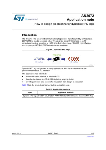
AN2972Application noteHow to design an antenna for dynamic NFC tagsIntroductionThe dynamic NFC (near field communication) tag devices manufactured by ST feature anEEPROM that can be accessed either through a low-power I2C interface or an RFcontactless interface operating at 13.56 MHz. Both short-range (ISO/IEC 14443 Type A)and long-range (ISO/IEC 15693) standards are supported.Figure 1. Dynamic NFC tags((3520 , & LQWHUIDFH5) LQWHUIDFHDL Dynamic NFC tag can be used in many applications, with the requirement that theprocessor features an I2C interface.This application note intends to: explain the basic principle of passive RFID describe the basics of a 13.56 MHz inductive antenna design provide guidelines for a successful integration, from design to production.Table 1 lists the products concerned by this application note.Table 1. Applicable productsMarch 2019TypeApplicable productsDynamic NFC tagsST25DV-I2C, ST25DV-PWM, M24LR and M24SR series Dynamics NFC TagsAN2972 Rev 91/26www.st.com1
ContentsAN2972Contents1Operating mode . . . . . . . . . . . . . . . . . . . . . . . . . . . . . . . . . . . . . . . . . . . . . 52Basic principles and equations . . . . . . . . . . . . . . . . . . . . . . . . . . . . . . . . 6342.1Passive RFID technology . . . . . . . . . . . . . . . . . . . . . . . . . . . . . . . . . . . . . . 62.2Simplified equivalent inlay circuit . . . . . . . . . . . . . . . . . . . . . . . . . . . . . . . . 82.3Basic equations . . . . . . . . . . . . . . . . . . . . . . . . . . . . . . . . . . . . . . . . . . . . . 92.4Optimum antenna tuning . . . . . . . . . . . . . . . . . . . . . . . . . . . . . . . . . . . . . 10How to design the antenna on a PCB . . . . . . . . . . . . . . . . . . . . . . . . . . 113.1Inductance of a circular antenna . . . . . . . . . . . . . . . . . . . . . . . . . . . . . . . .113.2Inductance of a spiral antenna . . . . . . . . . . . . . . . . . . . . . . . . . . . . . . . . . .113.3Inductance of a square antenna . . . . . . . . . . . . . . . . . . . . . . . . . . . . . . . . 123.4eDesignSuite antenna design tool . . . . . . . . . . . . . . . . . . . . . . . . . . . . . . 123.5PCB layout . . . . . . . . . . . . . . . . . . . . . . . . . . . . . . . . . . . . . . . . . . . . . . . . 143.5.1Length of the connections between dynamic NFC tag chipand antenna . . . . . . . . . . . . . . . . . . . . . . . . . . . . . . . . . . . . . . . . . . . . . . 143.5.2Ground, power, and signal layers . . . . . . . . . . . . . . . . . . . . . . . . . . . . . 143.5.3Metal surfaces . . . . . . . . . . . . . . . . . . . . . . . . . . . . . . . . . . . . . . . . . . . . 16How to check the NFC/RFID dynamic NFC tagantenna tuning . . . . . . . . . . . . . . . . . . . . . . . . . . . . . . . . . . . . . . . . . . . . . 184.1Antenna tuning measurements with a network analyzer . . . . . . . . . . . . . 184.2Antenna measurements with standard laboratory tools . . . . . . . . . . . . . . 195From design to production . . . . . . . . . . . . . . . . . . . . . . . . . . . . . . . . . . . 216Revision history . . . . . . . . . . . . . . . . . . . . . . . . . . . . . . . . . . . . . . . . . . . 242/26AN2972 Rev 9
AN2972List of tablesList of tablesTable 1.Table 2.Table 3.Table 4.Applicable products . . . . . . . . . . . . . . . . . . . . . . . . . . . . . . . . . . . . . . . . . . . . . . . . . . . . . . . 1K1 and K2 values according to layout . . . . . . . . . . . . . . . . . . . . . . . . . . . . . . . . . . . . . . . . 12Frequency compensation examples . . . . . . . . . . . . . . . . . . . . . . . . . . . . . . . . . . . . . . . . . . 16Document revision history . . . . . . . . . . . . . . . . . . . . . . . . . . . . . . . . . . . . . . . . . . . . . . . . . 24AN2972 Rev 93/263
List of figuresAN2972List of figuresFigure 1.Figure 2.Figure 3.Figure 4.Figure 5.Figure 6.Figure 7.Figure 8.Figure 9.Figure 10.Figure 11.Figure 12.Figure 13.Figure 14.Figure 15.Figure 16.Figure 17.Figure 18.Figure 19.Figure 20.Figure 21.Figure 22.Figure 23.Figure 24.Figure 25.Figure 26.4/26Dynamic NFC tags . . . . . . . . . . . . . . . . . . . . . . . . . . . . . . . . . . . . . . . . . . . . . . . . . . . . . . . . 1Dynamic NFC tag operating mode . . . . . . . . . . . . . . . . . . . . . . . . . . . . . . . . . . . . . . . . . . . . 5Dynamic NFC tag chip power mechanism in RF mode . . . . . . . . . . . . . . . . . . . . . . . . . . . . 6Power transfer versus reader/dynamic NFC tag orientation . . . . . . . . . . . . . . . . . . . . . . . . . 7Communication from the reader to the tag . . . . . . . . . . . . . . . . . . . . . . . . . . . . . . . . . . . . . . 8Communication from tag to the reader . . . . . . . . . . . . . . . . . . . . . . . . . . . . . . . . . . . . . . . . . 8Equivalent circuit of the dynamic NFC tag chip and its antenna. . . . . . . . . . . . . . . . . . . . . . 9Equivalent circuit of the dynamic NFC tag chip mounted on a loop antenna . . . . . . . . . . . . 9Tuning the dynamic NFC tag antenna . . . . . . . . . . . . . . . . . . . . . . . . . . . . . . . . . . . . . . . . 10Spiral antenna. . . . . . . . . . . . . . . . . . . . . . . . . . . . . . . . . . . . . . . . . . . . . . . . . . . . . . . . . . . 12Square antennas . . . . . . . . . . . . . . . . . . . . . . . . . . . . . . . . . . . . . . . . . . . . . . . . . . . . . . . . 12Antenna user interface screen design module of eDesignsuite . . . . . . . . . . . . . . . . . . . . . 13Correct PCB layout . . . . . . . . . . . . . . . . . . . . . . . . . . . . . . . . . . . . . . . . . . . . . . . . . . . . . . . 14Bad implementation - Example 1 . . . . . . . . . . . . . . . . . . . . . . . . . . . . . . . . . . . . . . . . . . . . 14Bad implementation - Example 2 . . . . . . . . . . . . . . . . . . . . . . . . . . . . . . . . . . . . . . . . . . . . 15Not recommended implementation . . . . . . . . . . . . . . . . . . . . . . . . . . . . . . . . . . . . . . . . . . . 15Acceptable implementation. . . . . . . . . . . . . . . . . . . . . . . . . . . . . . . . . . . . . . . . . . . . . . . . . 15Effect of metal surfaces on the antenna frequency tuning . . . . . . . . . . . . . . . . . . . . . . . . . 16Measurement equipment . . . . . . . . . . . . . . . . . . . . . . . . . . . . . . . . . . . . . . . . . . . . . . . . . . 18Example of the resonant frequency response of a prototype antenna . . . . . . . . . . . . . . . . 19ISO standard loop antenna . . . . . . . . . . . . . . . . . . . . . . . . . . . . . . . . . . . . . . . . . . . . . . . . . 19Setting up the standard laboratory equipment . . . . . . . . . . . . . . . . . . . . . . . . . . . . . . . . . . 20Example of a frequency response measurement of a prototype antenna . . . . . . . . . . . . . 20Application examples . . . . . . . . . . . . . . . . . . . . . . . . . . . . . . . . . . . . . . . . . . . . . . . . . . . . . 21Detuning effect . . . . . . . . . . . . . . . . . . . . . . . . . . . . . . . . . . . . . . . . . . . . . . . . . . . . . . . . . . 22Impact of housing/packaging material on RF communication . . . . . . . . . . . . . . . . . . . . . . 23AN2972 Rev 9
AN29721Operating modeOperating modeThe integration of dynamic NFC tag in an application is a straightforward task: on the I2Cside, the device must be connected to a master I2C interface (like any serial I2C EEPROMdevice), on the RF side, the dynamic NFC tag chip needs to be connected to an externalantenna to operate.Figure 2. Dynamic NFC tag operating mode'\QDPLF 1)& WDJ FKLS&RGH'DWD3DUDPHWHUV,'7UDFHDELOLW\([WHUQDO LQGXFWLYH DQWHQQD06Y 9 The design of an antenna for dynamic NFC tag is based on the placement of a loop on theapplication PCB. Its impedance matches the device internal tuning capacitance value(Ctuning) to create a circuit resonating at 13.56 MHz. The basic equation of the tuningfrequency is:1f tuning -----------------2Π L antenna C tuningAN2972 Rev 95/2625
Basic principles and equations2AN2972Basic principles and equationsDefinitionsTag: the dynamic NFC tag chip mounted on the PCB and connected to its antenna.Reader : an electronic device able to communicate with tags in RF mode.2.1Passive RFID technologyThe ISO 15693 and ISO 14443 RF protocols used by dynamic NFC tag devicesmanufactured by ST are based on passive RFID technology, operating in the high frequency(HF) range, at 13.56 MHz.Power transferWhen the dynamic NFC tag chip operates in RF mode, it is powered by the reader. Nobattery is required to access it in RF mode, neither in read nor in write mode. The dynamicNFC tag chip draws all the power it needs to operate from the magnetic field generated bythe reader through its loop antenna.The reader - tag system is similar to a voltage transformer, where the reader acts as theprimary winding, and the tag as the secondary winding.Reader and tag are magnetically and mutually coupled to each other.The energy transfer from the reader to the dynamic NFC tag chip depends on: how well the tag antenna is tuned, close to the reader's carrier frequency (13.56 MHz) the distance between the reader and the tag antenna board the dimensions of the reader antenna and of the tag antenna board the reader power the tag antenna orientation related to the reader antenna.Figure 3. Dynamic NFC tag chip power mechanism in RF mode'\QDPLF 1)& WDJ H[WHUQDO DQWHQQD'\QDPLF 1)& WDJ FKLS97DJ 9 VLQ ȦW% % VLQ ȦW5),' UHDGHU9 9 VLQ ȦW5HDGHU DQWHQQD06Y 9 6/26AN2972 Rev 9
AN2972Basic principles and equationsWhen the dynamic NFC tag is placed in the RFID reader’s electromagnetic field, the amountof energy powering the device is directly related to the orientation of the dynamic NFC tagantenna and to the RFID reader antenna. Indeed, this energy depends on how theelectromagnetic field lines generated by the reader flow through the dynamic NFC tagantenna (see Figure 4).This directly impacts the read range, more in detail: the best configuration is obtained when the antennas are parallel and face each other the read range drops to zero when the antennas are perpendicular to each other any other orientation is possible and will result in different read ranges.Figure 4. Power transfer versus reader/dynamic NFC tag orientation%HVW RULHQWDWLRQ '\QDPLF 1)& WDJ QWHQQD IDFLQJ WKH 5),'5HDGHU DQWHQQD:URQJ RULHQWDWLRQ '\QDPLF 1)& WDJ QWHQQD WDQJHQW WR HOHFWUR PDJQHWLF ILHOG% FFHSWDEOH EXW QRW RSWLPL]HG%%a%5HDGHU DQWHQQD06Y 9 Data transferWhen placed in a reader’s magnetic field able to power it, the dynamic NFC tag chipbuilt-in circuitry demodulates the information coming from the reader (see Figure 5).AN2972 Rev 97/2625
Basic principles and equationsAN2972Figure 5. Communication from the reader to the tag 7DJ DQWHQQD'\QDPLF 1)& WDJ FKLS5),' UHDGHU5HDGHU DQWHQQD06Y 9 At the end of the request, the reader keeps the magnetic field non modulated to power thetag, and allows it to generate an answer. To send its response back to the reader, thedynamic NFC tag chip backscatters the data to the reader by internally modulating its inputimpedance. Tag chip input impedance variation modulates the signal across the readerantenna due to the mutual coupling between reader and tag antennas. The readerdemodulates this signal and decodes the tag answer.Figure 6. Communication from tag to the reader P97DJ DQWHQQD5'\QDPLF 1)& WDJ FKLS 9 5),' 5HDGHU5HDGHU DQWHQQD06Y 9 All this is part of the standard protocol and is taken into account by the dynamic NFC tagchip embedded circuitry and by the RFID reader’s electronics.2.2Simplified equivalent inlay circuitFigure 7 shows the equivalent electrical circuits of the dynamic NFC tag and its antenna.8/26 Dynamic NFC tag chip is symbolized by a resistor Rchip representing its currentconsumption, in parallel with a capacitor Ctun representing its internal tuningcapacitance and internal parasitics. Measuring a loop antenna impedance evidences a self-resonant frequency. Thecorresponding equivalent model involves an inductance in parallel to a capacitance.Cant represents the overall stray capacitance of the loop antenna (including theAN2972 Rev 9
AN2972Basic principles and equationsassembly), Rant the resistive loss of the antenna and Lant the self-inductance of theloop antenna.Figure 7. Equivalent circuit of the dynamic NFC tag chip and its antenna 5FKLS&WXQ5DQW&DQW/DQW DQW%'\QDPLF 1)& WDJ FKLS([WHUQDO DQWHQQD06Y 9 Cant, Rant and Lant are constants but the resulting impedance (their parallel combination) isfrequency dependent. At self-resonance frequency, the imaginary part of the antennaimpedance Zant is null and Zant is purely resistive. Below the self-resonance frequency, theimaginary part of the antenna impedance is positive and the antenna behavior is inductive.The equivalent inductance of the antenna is defined LA as LA XA / ω for frequencies belowthe self resonant frequencies (Zant RA jXA).At low frequencies, where the impact of stray capacitance Cant is negligible, LA Lant(self-inductance). However, at 13.56 MHz the impact of stray capacitance cannot beneglected and LA Lant.2.3Basic equationsResonant frequencyFigure 8. Equivalent circuit of the dynamic NFC tag chip mounted on a loop antenna5 / 5V & 92&&V9 & & & QWHQQD'\QDPLF 1)& WDJ FKLS06Y 9 Figure 8 shows the equivalent circuit of an dynamic NFC tag chip mounted on a loopantenna in the presence of a sinusoidal magnetic field. VOC represents the open circuitvoltage delivered by the antenna, which depends on the magnetic field strength, theantenna size and the number of turns.AN2972 Rev 99/2625
Basic principles and equationsAN2972The tag antenna impedance is Zant RA jLAω, where LA is the antenna inductance.The dynamic NFC tag chip impedance is given by ZS RS j x 1 / CSω, where RSrepresents the power consumption of the chip, and CS represents the serial equivalenttuning capacitance, both converted in serial model.The resonant frequency of the equivalent RLC circuit is given by the condition LACSω2 1,where (ω 2 π f, f in Hz).2.4Optimum antenna tuningThe total impedance of the RLC circuit is Ztot Zant ZS.At resonant frequency LACSω2 1, the total impedance is reduced to Ztot RA RS (thetotal impedance of the antenna is minimal, the current inside the antenna and the voltagedelivered to the dynamic NFC tag chip are maximum), and the maximum energy is providedto the device.Figure 9 shows three examples of dynamic NFC tag antenna tuning.Tag #2 is the best tuned for this application configuration.Figure 9. Tuning the dynamic NFC tag antenna(QHUJ\5HDGHU DQWHQQD WXQLQJ7DJ DQWHQQD WXQLQJ7DJ DQWHQQD WXQLQJ7DJ DQWHQQD WXQLQJ 0 ]10/26AN2972 Rev 9&REQUENCYDL D
AN29723How to design the antenna on a PCBHow to design the antenna on a PCBA 13.56 MHz antenna can be designed with different shapes, depending on the applicationrequirements. As explained previously, the major parameter is the equivalent inductance LAof the antenna at 13.56 MHz.The stray capacitance is difficult to approximate, but for typical NFC/RFID products is in therange of few pF.For some antenna shapes, Section 3.1, Section 3.2, and Section 3.3 give useful formulas tocalculate the self-inductance Lant, even if the stray capacitance of the antenna is notestimated.Section 3.4 presents a calculation tool called Antenna Design, which is a part of theeDesignsuite, to calculate equivalent inductance of rectangular antennas taking intoaccount an approximation of the stray capacitance.3.1Inductance of a circular antennaL ant μ0 N3.21.9r r ln ---- , where:r0 r is the radius, in millimeters r0 is the wire diameter, in millimeters N is the number of turns µ0 4 π · 10–7 H / m L is measured in HenryInductance of a spiral antenna2a2L ant 31.33 μ0 N -----------------------, where (see Figure 10):8a 11c a (rin rout) / 2 (the average radius, in meters) c rout - rin is the thickness of the winding, in meters µ0 4 π · 10–7 H / m L is measured in Henry N is the number of turnsAN2972 Rev 911/2625
How to design the antenna on a PCBAN2972Figure 10. Spiral antennaFURXWULQ06 9 3.3Inductance of a square antennad2L ant K1 μ0 N ---------------------------- , where:1 K2 p d (dout din) / 2 in millimeters, where: dout outer diameterdin inner diameter p (dout – din) / (dout din) in millimeters K1 and K2 depend on the layout (refer to Table 2 for values)Figure 11. Square antennasTable 2. K1 and K2 values according to Octagonal2.253.55eDesignSuite antenna design toolTo easily develop the customer antenna, ST provides an antenna design tool, part ofeDesignsuite, available from the NFC product web page on www.st.com, to computerectangular antennas at 13.56 MHz.After entering some parameters related to the PCB material and antenna dimensions, thetool estimates the antenna equivalent inductance by calculating the self-inductance andestimating the stray capacitance of the antenna.12/26AN2972 Rev 9
AN2972How to design the antenna on a PCBFigure 12. Antenna user interface screen design module of eDesignsuiteFigure 11 shows an example of antenna computation, the following parameters have to bedefined: Antenna geometry parameters–Turns: number of complete turns (four segments per turn)–Antenna length, in mm–Antenna width, in mm–Number of layers (1 by default)Conductor parameters (copper is used by default)–Width of tracks, in mm–Spacing between turns, in mm–Thickness of the conductor, in µmSubstrate parameters–Thickness, in mm–Dielectric permittivityOnce the antenna equivalent inductance has been calculated, a prototype can be produced.The antenna design is validated measuring the antenna impedance (using an impedanceanalyzer, a network analyzer or an LCR meter) or measuring the tuning frequency of the tagusing a contactless method (see Section 4).AN2972 Rev 913/2625
How to design the antenna on a PCBAN29723.5PCB layout3.5.1Length of the connections between dynamic NFC tag chipand antennaThe dynamic NFC tag chip must be laid out as close as possible to the antenna (a fewmillimeters). Any additional wire/trace changes the antenna characteristics and tuning.3.5.2Ground, power, and signal layersThe layout of an inductive antenna on a PCB requires special attention: no copper planes above or below the antenna no copper planes surrounding the antenna.Figure 13 shows what can be considered the optimal layout: the dynamic NFC tag chip isclose to antenna, the ground plane is far from it.Figure 13. Correct PCB layout)URQW 3&% VLGH%DFN 3&% VLGH06Y 9 The energy transfer and the communication between the reader and the dynamic NFC tagare suitable because no copper planes overlap the antenna.Bad design examplesFigure 14 and Figure 15 show examples of incorrect design. In both cases, theelectromagnetic flux cannot flow through the antenna, consequently there is no energytransfer between the reader and the dynamic NFC tag antenna.Figure 14. Bad implementation - Example 114/26AN2972 Rev 9
AN2972How to design the antenna on a PCBFigure 15. Bad implementation - Example 2Figure 16 shows an example of a not recommended implementation. The electromagneticflux is greatly attenuated by the short-circuited loop surrounding the dynamic NFC tagantenna.Figure 16. Not recommended implementationFigure 17 shows an acceptable implementation, here the antenna and the ground plane donot overlap.Figure 17. Acceptable implementationAN2972 Rev 915/2625
How to design the antenna on a PCBAN2972It is recommended to allocate a dedicated area of the PCB layout to the antenna only, withno surrounding ground layer, as shown in Figure 13.3.5.3Metal surfacesWhen the antenna is placed close to a conductive surface, its self-inductance decreases. Asa consequence, the tuning frequency of the NFC/RFID tag increases, as shown inFigure 18.Figure 18. Effect of metal surfaces on the antenna frequency tuningϭϯ͘ϱϲϭϯ͘ϱϲ н džй& D,njͿ ϭϭ ůŽŐ ŵĂŐŶŝƚƵĚĞ Ě ĞŐĞŶĚ͗ &ƌĞƋƵĞŶĐLJ ƚƵŶŝŶŐ ŽĨ ĂŶ ĂŶƚĞŶŶĂ ŝŶ ƚŚĞ ŽƉĞŶ Ăŝƌ&ƌĞƋƵĞŶĐLJ ƚƵŶŝŶŐ ŽĨ ĂŶ ĂŶƚĞŶŶĂ ĐůŽƐĞ ƚŽ ŵĞƚĂůD ϯϬϳϯϵsϭIn addition to the tuning frequency drift, the tag quality factor decreases.When an antenna designed to work in free space has to operate close to a metal surface,the frequency tuning drift must be compensated to get 13.56 MHz tuning frequency in theenvironment.This can be achieved designing a new antenna with a larger equivalent inductance oradding an external tuning capacitance to the existing antenna.Table 3 shows an example of tuning frequency drift compensation using an external cap.Table 3. Frequency compensation examplesFeaturesANT1-M24LR16EANT1-M24LR16E with 74 pFin parallel to the antennaAntenna size45 mm x 75 mm45 mm x 75 mmFrequency tuning in the air13.7 MHz7.5 MHzFrequency tuning close to themetal surface (1)25 MHz14 MHzRead range in the open air (1)7.5 cm0.5 cmRead range close to the metalsurface(1)(2)No detection2.5 cmStatusThis antenna is tuned to operate This antenna is tuned to operatein the open airclose to metal1. The measurement has been done with the CR95HF RF transceiver board from M24LR-Discovery kit.2. The measurement has been done on an antenna stuck on the full metal table.16/26AN2972 Rev 9
AN2972How to design the antenna on a PCBAntenna redesign results in an increased number of turns: this is possible only whensufficient space is available on PCB, and requires time for the new development steps.When antenna redesign is not possible, an external capacitance has to be used.AN2972 Rev 917/2625
How to check the NFC/RFID dynamic NFC tag antenna tuning4AN2972How to check the NFC/RFID dynamic NFC tagantenna tuningDifferent parameters can impact the tuning frequency of the NFC/RFID tag: antenna equivalent inductance computation precision length of the connexion between the device and its antenna in application antenna environment (metal surface, ferromagnetic materials close to the antenna).It is then needed to check the resonant frequency of the NFC/RFID tag by measurement inthe final application conditions.4.1Antenna tuning measurements with a network analyzerThe tuning frequency of the dynamic NFC tag antenna can be measured using a networkanalyzer with a loop probe.The RF electromagnetic field is generated by connecting a loop probe to the output of thenetwork analyzer set in reflection mode (S11 measurement).Loop probe can come from the market, or be a self-made single turn loop made with acoaxial connector and a copper wire twisted at the end. Building the loop probe like thismakes it possible to adjust the size of the loop to the size of the tag antenna for a bettercoupling during the measurement.Figure 19. Measurement equipment.ETWORK ANALYSER,OOP PROBE!NTENNA PROTOTYPE WITH THE - ,2XX REPRESENTED AS A CAPACITORAI BThis equipment setup will directly display the system’s resonant frequency.ExperimentsThe following list of parameters shows an example of instrument setup for measurement: start frequency: 5 MHz end frequency: 20 MHz output power: - 10 dBm measurement: reflection or S11 format: log magnitude.Place the antenna within the field generated the loop probe connected to the networkanalyzer. During the measurement, loop probe and tag antenna are magnetically andmutually coupled. In presence of the tag, the mutual coupling causes a change in the loopprobe impedance.18/26AN2972 Rev 9
AN2972How to check the NFC/RFID dynamic NFC tag antenna tuningAt resonant frequency of the tag, loop probe impedance resistance reaches the maximumwhile the reactance returns to the self-resonance value; the loop probe impedance is nearly50 Ω, evidenced by a minimum on the S11 curve.Figure 20. Example of the resonant frequency response of a prototype antenna1212.51313.51414.51513.56 MHzS11 Logmagnitude(dB)Frequency (MHz)Resonant frequency (13.56 MHz)ai171994.2Antenna measurements with standard laboratory toolsThe antenna resonant frequency can also be measured with standard laboratory equipmentlike a signal generator, an oscilloscope and two standard loop antennas.Experiment setupConnect the first ISO 10373-7 standard loop antenna (see Figure 21) to the signalgenerator, to generate an RF electromagnetic field.Connect the second ISO 10373-7 standard loop antenna to the oscilloscope (see Figure 22)by using either a standard oscilloscope probe (1 MΩ or 10 MΩ input impedance) or a 50 ΩBNC cable (oscilloscope input set to 50 Ω in this case).Note:The ISO 10373-7 standard antennas can be replaced by self-made single turn loopantennas, whose size can be matched to the tested tag.Figure 21. ISO standard loop antennaISO/IEC 7810 ID-1 outline72 mm 42 mm coil1 turnconnectionsi15819AN2972 Rev 919/2625
How to check the NFC/RFID dynamic NFC tag antenna tuningAN2972Figure 22. Setting up the standard laboratory equipment2VFLOORVFRSH4 IDFWRU PHDVXUHPHQW VFKHPH6\QFKURQL]DWLRQ IUHTXHQF\7DJ WR EH PHDVXUHG ORRS DQWHQQD 0XVW EH WXQHG EHWZHHQ DQG 0 ]6LJQDO JHQHUDWRUDL EExperimentsPlace the tag in front of the loop antenna connected to the signal generator.When a magnetic field is present, a current flows into the tag antenna, this currentgenerates a magnetic field, which is captured by the second loop antenna connected to theoscilloscope. At the tag resonant frequency, the current flowing into the tag antenna, themagnetic field generated by the tag antenna and the voltage amplitude displayed by theoscilloscope are at their maximums.Set the signal generator to output a sine wave with a peak-to-peak amplitude in the range of200 mV. Starting from 5 MHz, increase the signal generator frequency until you reach themaximum amplitude of the signal measured with the oscilloscope, then the signal generatorfrequency corresponds to the resonant frequency of the tag.Figure 23 provides the frequency response curve of the prototype antenna, which is basedon measurement of the received signal amplitude at different frequencies.Figure 23. Example of a frequency response measurement of a prototype antennaResonant frequency 13.56 MHzVoltage onthe secondISO 10373-7antenna1212.51313.5Frequency (MHz)20/26AN2972 Rev 91414.515ai17300
AN29725From design to productionFrom design to productionDesigners must expect some differences between the theoretical and the real performanceof the antenna on the PCB in the end application. Here are a few considerations.System level validationTake great care when validating the antenna tuning for the various application use cases,programming traceability information on the manufacturing line, performing inventory ofseveral end-products in the warehouse and reading data (end user).Different reader profiles result in distinct performance levels on a given dynamic NFC tagboard.Figure 24. Application examplesai17184Considerations on the actual system tuning frequencyEven though all readers transmit at 13.56 MHz, the optimal tuning frequency of theM24LRxx or ST25DVxx antenna is not necessarily 13.56 MHz.Some mutual mechanisms such as detuning/coupling between the reader antenna and thetag antenna may lead to an dynamic NFC tag chip antenna with an optimum tuningfrequency different from 13.56 MHz.A good example is ST’s reference antenna (Gerber files available from www.st.com), whosetuning frequency is 13.74 MHz(a) to provide the best performance with the FEIGELECTRONIC MR101 reader.a. Using the method described in Section 3.5.3: Metal surfaces.AN2972 Rev 921/2625
From design to productionAN2972The read range varies, depending on whether the dynamic NFC tag board is read alone orstacked with others (detuning effect). Figure 25 illustrates the detuning effect.Figure 25. Detuning effectThe vicinity of another dynamic NFC tag board may change the inductance dynamics. Theboards may couple with each other, leading to a resultant antenna resonant frequencydifferent from the individual one.These are just examples of what may induce a difference between theory and real usecases. They are meant to emphasize the need for real life validation of antenna designs.PCB manufacturing process validationThe PCB fabrication parameters (such as the copper or epoxy layer thickness) have animpact on the antenna inductance. Variations happen if the parameters of the PCBfabrication process change or in case of a change of PCB supplier.Product packaging/housing considerationsThe read range of the dual interface dynamic NFC tag board can be greatly affected by thehousing of the final product.The most obvious case is when a metallic housing is used. The product packaging thenbehaves as a Faraday cage, preventing the reader energy and signal from attaining the dualinterface EEPROM device.The housing also influences the PCB antenna’s tuning frequency, for this reason, it isalways recommended to measure the RF performance of the application in the final productconfiguration.22/26AN2972 Rev 9
AN2972From design to productionFigure 26. Impact of housing/packaging material on RF communicationDual interface EEPROMNonconductive housing:RF communication OKConductive housing:no RF communicationai17301Process flow Design:–Start from the dual interface EEPROM’s internal tuning frequency (Ctuning).Hint: check the device datasheet.–Calculate the theoretical Lantenna value based on Ctuning and ftuning.Hint: use the simplified models in this application note or other more sophisticatedmodels developed in the RF literature. –Define the antenna dimensions.–Compute the theoretical antenna design and layout.Prototyping–Define an antenna matrix with different values centered around the targetedLantenna value.Hint: select 6 to 10 antennas with inductances that vary around Lantenna by stepsof 5 %.–Fabrication of the antennas and dynamic NFC tag chip mounting.For each prototype: –Measure the antenna tuning frequency.–Measure the read range with all types of selected RFID readers.–Measure the read range in configurations close to the actual pr
The design of an antenna for dynamic NFC tag is based on the placement of a loop on the application PCB. Its impedance matches the device internal tuning capacitance value (C. tuning) to create a circuit resonating at 13.56 MHz. The basic equation of the tuning frequency is: f. tuning. 1. antenna. C. tuning