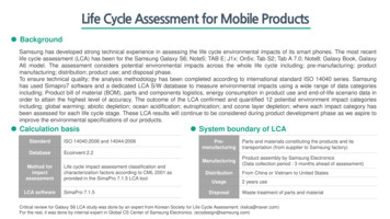
Transcription
The missingSamsung EVO 840 - 250 GB SSDRepair ManualFirst version: July 2016Current version: 27.04.2018IntroductionUnfortunately my Novena laptop got physically damaged, so I took the SSD (Solid-State-Disk)from the Novena to a data-recovery company, who analyzed the SSD and discovered that the SSDhas a problem in its startup phase that is most likely due to a firmware corruption, but the physicaldamage is actually not a problem for the SSD.According to the company it is very likely that all other Novena SSDs (in Laptops, Desktops andHeirlooms) with the same firmware have the same problem and might also loose data.Therefore I started to work on analyzing the firmware, and the firmware update process.I have created the following guideline how you can extract and verify the firmware from your SSD,so that we can find out together, which models are actually affected.I will try to explain what you can do to protect your own SSD, or recover if the same or a similarproblem happens to your SSD.What you should do now:* Backup your data! But not to a SSD. SSDs seem not to be very well suited for backups from mypoint of view, I would suggest to use HDDs (Hard-Disk-Drive) instead.What you should do when such a problem happens to your SSD:Check back here, perhaps we have a solution for it already.If you need urgent access to your data, search for a data recovery company that has a PC-3000 SSDfrom AceLabs available, at the moment of this writing, I think it is likely that they could recoveryour data with it.This is how the problem of my SSD looks like from the kernel point of view (the following is theoutput from the “dmesg” command under Linux):[1.203395] ahci-imx 2200000.sata: fsl,transmit-level-mV value 1025, using00000024[1.203432] ahci-imx 2200000.sata: fsl,transmit-boost-mdB value 0, using00000000[1.203464] ahci-imx 2200000.sata: fsl,transmit-atten-16ths value 8, using00002800
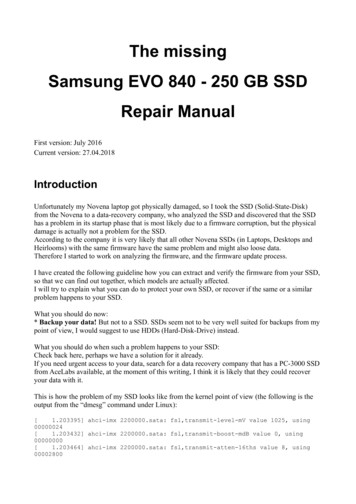
[1.203494] ahci-imx 2200000.sata: fsl,receive-eq-mdB not specified, using05000000[1.203543] ahci-imx 2200000.sata: Looking up target-supply from device tree[1.206436] ahci-imx 2200000.sata: SSS flag set, parallel bus scan disabled[1.206494] ahci-imx 2200000.sata: AHCI 0001.0300 32 slots 1 ports 3 Gbps 0x1impl platform mode[1.206531] ahci-imx 2200000.sata: flags: ncq sntf stag pm led clo only pmppio slum part ccc apst[1.208050] scsi host0: ahci platform[1.208473] ata1: SATA max UDMA/133 mmio [mem 0x02200000-0x02203fff] port0x100 irq 71[.][6.592593] ata1: link is slow to respond, please be patient (ready 0)[11.212587] ata1: COMRESET failed (errno -16)[16.602585] ata1: link is slow to respond, please be patient (ready 0)[21.222578] ata1: COMRESET failed (errno -16)[26.612582] ata1: link is slow to respond, please be patient (ready 0)[56.252588] ata1: COMRESET failed (errno -16)[56.261143] ata1: limiting SATA link speed to 1.5 Gbps[61.292587] ata1: COMRESET failed (errno -16)[61.301345] ata1: reset failed, giving up[61.310158] ahci-imx 2200000.sata: no device found, disabling link.[61.319008] ahci-imx 2200000.sata: pass ahci imx.hotplug 1 to enable hotplugSo it seems the SATA (Serial AT Attachment) host tries to initiate the communication withCOMRESET (somewhere between second 1.206531 and second 1.208473), but it never receivesthe COMINIT answer the SSD should give. 5 seconds later at second 6.592593 is complains thatthere is still no answer and a minute later at second 61.301345 it gives up. Theoretically theCOMINIT should come within a second after the COMRESET.If you are interested in the details of the SATA protocol, I can recommend this 21/sata-protocolOn page 30 you can see the timing of COMRESET and COMINIT. The SATA host (computer)should start with COMRESET, and the SSD should reply with COMINIT.Afterwards they can calibrate, negotiate the speed, and then they have a “link”.From OCZ SSDs I have heard that they have some kind of panic lock, where the SSD stops bootingto prevent further damage when it discovered a potential problem. This behaviour on OCZ SSDs isoften triggered when waking up a Laptop from hibernation. It could be that this is an instance of asimilar panic lock for Samsung SSDs.Layer 0 - Physical layerOk, let's start with the physics.The SSD is contained in a metal case, to open it you have to open 3 screws, one ofthem is visible, the other 2 are behind the plastic sticker.The screw has a Pentalobe format, so you need a Pentalobe screwdriver.I found a working one in the it/IF145-299-1(It's a bit funny that you need a 64 Bit Driver kit to access a 32 Bit CPU ;-)When you have opened it, the SSD PCB (Printed-Circuit-Board) should look like Image 1:the one on the upper right hand side of this image:Pentalobe
So what do we have here?The long thing on the upperend is the SATA connector, thebig square chip on the bottomleft is the controller CPU, inthe middle we have someSDRAM and on the right sideis the actual NAND Flashstorage chip.SATA ConnectorControllerRAMNANDFlashOn the back side is the secondNAND Flash chip in the samelocation (I guess that makes iteasy to route the traces,UART perhaps the address lanes areshared)Another thing that stronglyJTAGsuggests to put 2 NAND Flashchips on directly oppositesides of a PCB is the temperature sensing. You want a connection that is as short as possible fromthe temperature sensor to the NAND flash chips where the temperature has to be measured. Theeasiest way to achieve that is by placing the NAND flash chips at the same location, and thetemperature sensor directly next to both of them. (The temperature connection is done by theground plane in the PCB or a very wide trace)The controller CPU (the one one the left side of the image) is called Samsung MEX (the productnumber is S4LN045X01-8030), it has 3 ARM Cortex R4 cores, which are based on the ARMv7-Rarchitecture, and likely have about 400 MHz. MEX is the fifth generation of the chip, MAX was thefirst one, MBX the second one, .The following things are written on the controller CPU:SAMSUNG S4LN045X01-8030N7Y89MMBU1441 ARM 1441 means it was produced in the year 2014/Week 41It is said to have an 8 channel controller, if you want to learn more about what that means, I suggestthe following tecture-channels-and-banksThe SDRAM chip:Samsung 512 MB Low Power DDR2 SDRAMSamsung, 4Gb, LPDDR2 SDRAM, 1CH x 32, 8 banks, 134-FBGA, MONO, 1066Mbps,1.8V/1.2V/1.2V:512MB LPDDR2 DRAM:The following things are written on it:SAMSUNG 440K4P4G324EQ-FGC2K: Memory4: DRAMP: LPDDR2 (guess)4G: 4G, 8K/64ms Density32: x32 Bit Organisation
4: 8 internal BanksE: Interface ?Q: SSTL-2 1.8V VDD, 1.8V VDDQ-F: 7th GenerationG: FBGA PackageC: Commercial, Normal Temperature&Power range (095 C)EXH382HCCAnd now the NAND chips that actually hold your data:NAND TLC 128 GB: (19nm Toggle Mode 2.0 TLC (3-bit per cell) NAND (Model#K90KGY8S7M-CCK0))SAMSUNG 440K90KGY8S7M-CCK0K: Memory9: NAND Flash0: 3-Bit MLC (TLC)KG 128GY8 Organisation x8?S Voltage ?7 Mode ?M 1st GenerationC CHIP BIZ D : 63-TBGAC Commercial, Normal(0 C-95 C) & Normal PowerK Customer Bad Block ?0 Pre-Program Version:NoneI measured the voltages and connectivity of a very similar PCB which uses the same Controller andslightly different Flash chips to create a pinout:http://www2.futureware.at/ philipp/ssd/K9CHGY8S5M-CCK0-Pinout.pdfThe chip has 0.8mm pitch and BGA-316 form factor.
The only product selection guide that contained relevant information that I could find was from2010, so it did not contained all variations, but it is still a helpful guide to understand Samsung snaming /semiconductor/file/media/SamsungPSG july2010 final2.pdf - Page 16If anyone can provide any further information to explain the variations we have here, I would beinterested to hear.Unfortunately at first I couldn't find datasheets for any of the other chips used on the SSD.There are a few smaller chips on the PCB: JS4TAA and AKE4QD, "ABS 431 .WD"There is also a Chip named "GUILL TI 48" on it, which is from Texas re/ccrz ProductDetails?viewState DetailView&cartID &sku TEX-GUILL PKG 2&store DefaultStorefzabkar from forum.hddguru.com has identified the chips and provided the following information:
“The mystery components appear to be marked especially for Samsung.JS4TAA appears to be a 5V STEF4S electronic fuse manufactured bySTMicroelectronics. "JS4" appear to be the important characters in the part number.GUILL is a TPS62130D2 synchronous step-down DC-DC converter manufactured byTexas Instruments.AKE40D appears to be a multiple-output switchmode DC-DC converter, probably withintegrated power sequencing. "AKE" appear to be the important characters in the partnumber.I'm guessing that the ABS part is an SPI flash memory.”The ABS part is actually not a SPI flash, but a I2C device, and my current guess is that it is thetemperature sensor, similar to those fhttp://www.nxp.com/documents/data en/DeviceDoc/25095A.pdfI logged the following I2C communication with an 01,Write,18,08 d,18,00 77,N,1.0923408E-01,Write,18,01 02 29,Y,1.0949680E-01,Write,18,04 05 d,18,05 50,N,1.1008976E-01,Write,18,02 05 d,18,05 00,N,1.1068304E-01,Write,18,03 04 d,18,04 B0,N,On (another?) SSD I got the following I2C traffic for every Smart command:Write 0x30 Data 05hRead 0x31 Data 22h 2ChSo 0x05 is obviously the command to read out a single temperature value, and for the temperaturevalues we read, we got the following table:22 A8 42 C22 88 40 C22 48 36 C22 3C 35 C22 38 35 C22 34 35 C22 2C 34 C22 28 34 C22 20 34 C22 20 34 C22 20 34 C22 24 34 C22 1C 33 C22 1C 33 C22 18 33 C
With the 2 constants 0x30 followed by 0x31 I was able to identify the I2C code in the firmware.On the various SSDs from Samsung the ABS part, or a similar chip is always located directlybesides the Flash chips on the PCB, which is necessary to measure the temperature. (You could puta SPI flash anywhere on the board)I found the following document which explains the thermal management strategy of Samsung withtheir newer 950 series starting at page sd/downloads/document/Samsung SSD 950 PRO White paper.pdfSo the thermal management that is used in the EVO840 is likely similar but not that advanced.Later on the actual “ABS” chip was found by fzabkar:MCP9844T-BE/MNY, Microchip, /-1 degC, 1.8V Digital Temperature Sensor, marking eviceDoc/20005192B.pdfLayer 1 - Link layerSSD's need to be electrically powered, this one needs to be powered through the SATA port.At first I used a USB-SATA adapter for supplying power.One relevant topic regarding the power-supply is the grounding for the JTAG port:I tried to attach the USB-SATA adapter to the USB power of a secondary laptop, and there Imeasured a nearly constant 2 Volt difference between the GND (ground) of the SSD and the GNDof the Novena.The signal level of the GPIOs of Novena is 3.3 Volts, so I thought that - 2 Volts could be too muchfor proper signaling reception.When I plugged the USB adapter into a USB port of the Novena, both Novena and SSD had thesame GND level (0 Volt difference).The downside of the USB-SATA adapters is that you do not get access to the initializationcommunication so PCI SATA adapter or SoC is preferred if you want to analyze the SATA behavior.I powered the SSD and measured all the voltages on all the Pins I could find, first on a good SSD,documented on printed up-scaled photos and then verified them on my broken SSD, and thevoltages were all OK.The voltages on the SATA Data pins were identical too, so I have some more confidence that theproblem is not a physical problem of the SATA interface, and that all the power-management isgood.You can measure the power with a multi-meter on various places. Make sure that you configureyour multi-meter correctly to read voltages, and that you always touch only a single pin, that you donot short out 2 pins next to each other. When you have sharp probe heads, make sure you do notpush too hard on the pins, to not squish the pins!
SAFEI have created a separate PDF with both front-side and backside images where you should be able tobetter zoom in so that you can look at the details:http://www2.futureware.at/ philipp/ssd/SamsungEVO840Voltages.pdfLater on I took an Arduino with a 4-Relais shield and connected 2 power cables to it, so that I canswitch on/off the SATA power supply (one relais for the 5V rail and one relais for the 12V rail, andfinally one relais for the Safe-Mode) programmatically by sending switch on/off commands to theArduino. Nowadays I would recommend a dedicated USB relais board with at least 4 ports, I don’tlike the connection between the Arduino and the relais board, it isn’t very stable.Controlling the SATA data port was done later on by using a USB-SATA converter connected to theUSB port on the Novena, which can be controlled with the novena-usb-hub tool. (It enables/disablesthe power supply to the USB port)
JTAGNow regarding the JTAG interface:I found the JTAG pinout of the Samsung SSD on 28033114112(Thanks a lot to bsmtiam!)I found some more pins on the board:There are 2 pins right next to the JTAG interface (which I marked 0V, 1.8V TRST on the secondphoto). The one next to the JTAG pins is a RESET line (TRST/RESET).Later on I found that ACE Laboratory (makers o
Samsung EVO 840 - 250 GB SSD Repair Manual First version: July 2016 Current version: 27.04.2018 Introduction Unfortunately my Novena laptop got physically damaged, so I took the SSD (Solid-State-Disk) from the Novena to a data-recovery company, who analyzed the SSD and discovered that the SSD has a problem in its startup phase that is most likely due to a firmware corruption, but the