Transcription
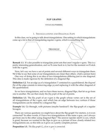
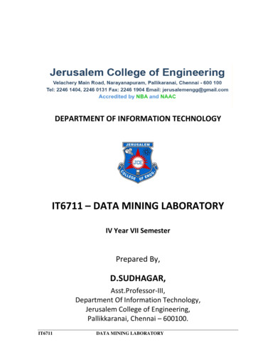
Physics 331, Fall 2008Lab VI - Exercises1LABORATORY VI : Flip-Flops1Reading:SimpsonSect. 12.1 - 12.5, 12.8.6 - 12.8.7Sect. 13.1 - 13.5Optional reading:Horowitz & HillSect. 8.01 - 8.03, 8.16 - 8.18.IntroductionIn this lab we will explore some digital electronics focusing especially on flip-flop circuits. A flipflop circuit is a binary memory element and forms the basic building block for many memorysystems, counters, and other sequential logic circuits, i.e. circuits that respond to a series of inputsrather than merely the present input. A flip-flop has two output terminals and two stable voltagestates. When operating correctly, if one of the output terminals is in a high voltage state the otheroutput terminal is in a low voltage state. The output voltages of the two terminals can be flipped(exchanged) very quickly by applying a single input pulse to an appropriate input terminal. Thenew ”flipped” state of the output terminals is then stable, i.e. it persists even after the input pulsehas ended.2Laboratory Preliminaries2.1Lighting LEDsIn the following lab exercise we will be monitoring the output state of our logical devices usinglight-emitting diodes (LEDs).220ΩNANDgatelight emittingdiode (LED)Figure 1: NAND output monitored using an LEDAn example is shown to the left, where wemonitor the output of a NAND gate. TheLED will be lit (dark) when the output isin the high (low) state. The 220 Ω resistorin series with the LED controls the currentthat is drawn from the NAND gate outputand, therefore, the LED brightness. A fewtens of milliamps is usually adequate andwill not harm the output transistors of the74LS chips (TTL logic) we will be studying.On the right hand side of your breadboard there are pre-installed eight LEDs, labeled LED 0 throughLED 7, each already connected in series with its own 220 Ω resistor. For example, to construct theabove circuit, you would only need to attach the NAND gate’s output to the LED 0 input on thelower right-hand side of your breadboard.If you prefer, there are LEDs available in colors other than green and you may use them instead.The ”low port” of the light emitting diodes can be recognized by having a flat part on the plastichousing and also a shorter pin (when new). That is, when building the circuit ground should be
Physics 331, Fall 2008Lab VI - Exercises2connected to the shorter of the two LED pins and then the flat part will point to ground. Thisensures forward bias of the LED and it will light up.2.2Handling ICsRemember to always turn off the power on your breadboard before installing or removing an integrated circuit (IC). Also, please use the available tools to install and remove the IC circuits. Doingthis by hand will very often bend the pins.33.1Lab ExercisesNAND gate Logica) Connect a 74LS00 four two-input NAND gate to power (see Fig. 2) and verify for one of thegates that it obeys the NAND truth table. To do so, attach the output to an LED and the inputsto either 0V or 5V.b) Connect several NAND gates together to make an OR gate and verify its correct operation, i.e.,determine the truth table. 5V131412111089VDD7400VSS1234567Top ViewFigure 2: Quad 2-Input NAND gate3.2Set-Reset Flip-FlopBuild the set-reset flip-flop shown in Fig. 3a. As indicated in the figure, the inputs to this circuit,labeled S̄ and R̄, are active low, meaning that a change of the output Q results from switching theinput from high ( 5 V) to low (0 V).
Physics 331, Fall 2008Lab VI - Exercises3Investigate the properties of the SR flip-flop by testing a variety of input sequences and noting theresults.a) Start with both inputs in the high state. What is Q and Q̄? Leave R̄ high, take S̄ to the lowstate and back to high. What happens to Q and Q̄? Repeat this operation several times.b) Now leave S̄ high, take R̄ to the low state and back to high. What happens to Q and Q̄?c) Try various other input sequences and summarize your observation.d) Try grounding both inputs of the flip-flop, then returning them simultaneously to high. Whathappens? (This input state is never used and is called indeterminate)a) 5 Vb)SQ1kΩOutHighLowQR1kΩ 5 VFigure 3: a) Set-Reset Flip-Flop b) NAND debounced switch3.3Switch Debouncing using a Flip-FlopAn important application of flip-flops is as “debouncers” for switches. A NAND based debounceris shown in Fig. 3b. Build this circuit and show that it works as you expect. (Can you explain howit works? Is the switching clean? Is it fast?)Don’t take the circuit apart, we’ll need it for the next exercise.3.4Divide-by-Two with D Flip-FlopThe 74LS74 circuit, shown in Fig. 4, contains two independent positive-edge clocked D flip-flops.In these flip-flop circuits, the data input at D is passed to the output Q (and as inverted signal tothe complement Q̄) whenever the clock signal at CLK makes a transition from low to high. ThusQ only changes when CLK makes a positive transition. For normal operation the SET and CLRinputs must be held high.a) Connect the output of the debounced switch to the clock input CLK, as shown in Fig. 5a. Verify(and report) that the input state of D, for both low and high inputs, can be passed only for positive
Physics 331, Fall 2008Lab VI - Exercises47474 5V2CLR13142D122Q82Q2CLK 2SET11109VDDDCLRCLKSETDQQCLRQCLK QSETVSS121CLR 1D431CLK 1SET61Q51Q7Top ViewFigure 4: 74LS74: Dual D Edge-Triggered Flip-Flopgoing clock signals. Is Q̄ the complement of Q?b) Make a divide-by-two circuit as shown in Fig. 5b. Using the debounced switch check the operation. Does it work as expected? Now, disconnect the debounced switch from the clock and drivethe clock with the “sync out” square wave from your signal generator at about 10 kHz. Observethe clock signal and the output simultaneously on the scope.c) Make a divide-by-four circuit by appropriately wiring two D-flip-flops. Demonstrate that yourcircuit works. To explain how the final output at one-fourth the input frequency is produced, recordone-by-one the input signals and output signals and use these observations to sketch a ”timing diagram” (for an example see Simpson pg. 625) .Don’t take the circuit apart, we’ll need it for the next exercise.a) 5 Vb) 5 VCLR 5V or 0 VCLRQDto LED74LS74fromDebouncerSET 5 VOUT74LS74QCLKQDto LEDINQCLKSET 5 VFigure 5: a) Set-Reset to test 74LS74 Flip-Flop b) Divide-by-Two with D Flip-Flop
Physics 331, Fall 20083.5Lab VI - Exercises5MultiplexersA multiplexer is the electrical analog of a rotary mechanical switch. It allows one to select one ofseveral input lines and connect it to the output. A demultiplexer does the reverse, it allows one toroute an input to one of many output lines. Digital electrical multiplexers are unidirectional andone has to buy different IC chips for multiplexing and demultiplexing or purchase integrated chipswith both capabilities. These latter IC chips are also simply called multiplexers. Such circuits areessential in many applications. For example in digital communication applications, the data that isto be transmitted is often represented by eight bits ( “byte”) and it needs to be send over a singlewire, i.e. the byte must be sent one-bit at a time. This general problem is called parallel-to-serialconversion and is solved electronically by a multiplexer.There are also analog electrical multiplexer, which are typically bidirectional, allowing current flowin either direction. In this lab you will explore the operation of the 4051 analog electrical multiplexer(analog MUX). The 4051 is a single 8-Channel multiplexer having three binary control inputs, A,B, and C, and an inhibit input (see Fig. 6). The three binary signals (A, B, C) select 1 of 8 channelsIN/OUTIN/OUTto be Pinoutsturned on, and connect1 55 5 one of the12 012 3 8 outputs to the input.X CHANNELS11 AINH 6a)INH 6CD4051B (PDIP,VEECDIP,SOIC, TSSOP)10 B7TOPVIEW9 CV8b)SS4 116 VDD6 215 2COM OUT/IN 314 17 413 0CHANNELSIN/OUTCHANNELSIN/OUT5 512 3INH 611 AVEE 710 BVSS 89 CINHIBITINPUT STATESV8SSCCD4053B (PDIP, CDIP, TSSOP)CD4051BY CHANNELSTOP VIEW016 VDDbx 2IN/OUT IN/OUTCHANNELS00ax OR ay14 OUT/INY CHANNELScy 3OUT/IN CX OR CY 40 ay13IN/OUT CX 5120 axINH 611 AVEE 710 BVSS 89 CIN/OUT1B†10†9†1 14 13 401 5INH 630412 011 3015106011171 TSSOP)XCD4053B (PDIP, CDIP,TOP VIEWCD4052BXXNoneVEE 7VSS 8CD4051BCHANNEL IN/OUT74016 VDD65432B010 A9 B1000x, 0y11x, 1y014 OUT/IN ax1 OR ay0TG2x, 2yOUT/IN CX OR CY 4013 ay13x, 3yIN/OUT CX 5112 axXNoneLOGICLEVELCONVERSION1TGIN/OUTXTGCD4053B11 AINHIBITA OR B OR C0010 BVBINARYEE 7TOVSS1 OF 88DECODERWITHINHIBIT09 C11X77 VEE462† All inputs are protected by standard CMOS protection network.5541COMMONOUT/INTGay or by or cyax or3 bx or cxNoneTGCD4051BTGCHANNEL IN/OUT8 16VSS VDDTGTGX Don t Care6X CHANNELSIN/OUTAbx0 OR5015 1 OUT/IN12 1514 by132X CHANNELSIN/OUT2 13 COMMON “X” OUT/IN11Functional Block DiagramsINH311INH 6C16 VDD0 15 22 200cy 3†0“ON” CHANNEL(S)0IN/OUT16 VDD bx 2A10IN/OUT 1INHIBIT11AIN/OUTCDIP, TSSOP)TOPVIEW9 B10 A0 10COMMON0 “Y” OUT/IN015 OUT/IN bx OR byby 1c)BIN/OUT 00by 1Functional Block Diagrams11 3TRUTH TABLES(PDIP,VEE 7CD4052B312215114013TGFigure 6: The 4051 analog multiplexer: a) pinout diagram, b) truthtable, c) function block diagram. (Adapted from4051 datasheet [1])TG2A † 11TGBC††109LOGICLEVELCONVERSIONBINARYTO1 OF 8DECODERWITHINHIBITTGTGTGCOMMONOUT/IN3
Physics 331, Fall 2008Lab VI - Exercises6Control of analog signals up to 20 Vpp can be achieved by digital signals, if the digital signalamplitudes are at least 4.5V. More precisely, if the digital supply voltage range is larger 4.5 V(VDD VSS 4.5 V), then analog output swings are possible with amplitudes set by the supplyvoltage range VDD VEE and VDD VEE 20 V. The advantage of analog multiplexers is thatthey have a low ON impedance and very low OFF leakage current.In this lab you will use an analog multiplexer to build a digitally controllable amplifier. This is avery useful circuit because in many measurement applications the gain of the input circuitry hasto be adjusted depending on the amplitude of the incoming signal in order avoid clipping of theamplified output signals (oscilloscopes are an example).a) On resistance: Measure the On-resistance of output channel 3 of the 4051 analog MUX.For a possible approach recall last week’s lab, where you determined the on-resistance of the 4066analog switch. Note that you need to connect VDD to 5V, VSS and Inh to ground, and you needto set the input bits (A, B, C) such that output-channel 3 is selected. You may connect VEE toground or -15V. Does your result agree with the datasheet?b) Analog voltage range: Connect VDD to 5V and VSS , Inh, and VEE to ground. Pick theinput bits (A, B, C) such that output channel 3 is selected. Use a 411 opamp to implement a unitygain buffer. Connect the buffer’s output to the “Analog In” channel of the multiplexer and thebuffer’s input to the function generator (Tektronix CFG 280). For a sinusoidal input wave, measurethe multiplexer output (channel 3). What is the output voltage range? Does this agree with youexpectations? How can you change your circuit to increase the output voltage range? Do it andquantify the result.c) Digital Gain Control: Rewire the 411 opamp used for the unity gain buffer and build theinverting amplifier with digital gain control shown in Fig. 7. (Note that VEE - 15V). Pick theresistances R0-R3 such that gains of one, two, three, and four are achieved. Test your circuit anddiscuss the result. (Does it work as expected? Are there potential issues with this circuit?)You may test the circuit, for example, by connecting the MUX’s digital-inputs A and B to theinput line (CLK) and output line (Q) of the divide-by-two circuit you constructed previously andby observing the amplifier output on the oscilloscope. Make sure you drive the divide-by-two circuitusing square-waves with amplitudes in between 0 and 5 V. It is recommended that you use thesync-out signal of the signal generator and frequencies of around 100 Hz. Since a TTL gate (divideby-two circuit) is used to drive a CMOS gate (4051 MUX), difficulties may arise because the 3.5 VTTL output-high is barely high enough for CMOS logic. Therefore it is recommended to use a pullup resistor as shown in Fig. 7 before connecting to the A and B inputs of the CMOS 4051 MUX.References[1] CD4051B datasheet, Texas Instruments Incorporated, 2000. (Available, for example, from 051.pdf.)
Physics 331, Fall 2008Lab VI - Exercises7 5V20Kr 5VVin10KVout10K16VDD134051 MUX0R0141R1152R2123R3Analog In3 5V 5V1KDig Into 5VCMOSTTLA1114B1055C926Inh647VEEVSS78 15VFigure 7: The 4051 analog multiplexer: “rotary control” type schematic of 4051 used to implement an invertingamplifier with digital gain control.
LABORATORY VI : Flip-Flops Reading: Simpson Sect. 12.1 - 12.5, 12.8.6 - 12.8.7 Sect. 13.1 - 13.5 Optional reading: Horowitz & Hill Sect. 8.01 - 8.03, 8.16 - 8.18. 1 Introduction In this lab we will explore some digital electronics focusing especially on ip-op circuits. A ip-op circuit is a binary memory element and forms the basic building block for many memory systems, counters, and other .