Transcription
Double Data Rate (DDR) Memory DevicesEdward J. Wyrwasedward.j.wyrwas@nasa.gov301-286-5213Lentech, Inc. in support of NEPPAcknowledgment:This work was sponsored by:NASA Electronic Parts and Packaging (NEPP)Presented by Edward J. Wyrwas at the 2018 NEPP Electronics Technology Workshop (ETW), NASA GSFC, Greenbelt, MD, June 18-21, 2018.1
ARMBGABOKCANCBRAMCCICGACMOSDefinition1 MegabitThree DimensionalThree Dimensional Integrated CircuitsAbsolute Contacting EncoderAnalog to Digital ConverterAutomotive Electronics CouncilAdvanced Encryption StandardAir ForceAir Force Research LaboratoryAir Force Space and Missile Systems CenterAgile Mixed SignalARM Holdings Public Limited CompanyBall Grid ArrayBody of KnowledgeController Area NetworkConductive Bridging Random Access MemoryCorrect Coding InitiativeColumn Grid ArrayComplementary Metal Oxide SemiconductorCNXilinx ceramic flip-chip (CF and CN) packages are ceramic columngrid array (CCGA) packagesCOTSCRCCRÈMECRÈME MCCSECUD-CacheDCUCommercial Off The ShelfCyclic Redundancy CheckCosmic Ray Effects on Micro ElectronicsCosmic Ray Effects on Micro Electronics Monte CarloCrypto Security EnginControl Unitdefered cacheDistributed Control UnitDDRDouble Data Rate (DDR3 Generation 3; DDR4 Generation 4)DLADMADMEADoDDOEDSPdSPIDual Ch.ECCEEEEMACEMIBESAeTimersETWFCCUFeRAMDefense Logistics AgencyDirect Memory AccessDefense MicroElectronics ActivityDepartment of DefenseDepartment of EnergyDigital Signal ProcessingDynamic Signal Processing InstrumentDual ChannelError-Correcting CodeElectrical, Electronic, and ElectromechanicalEquipment Monitor And ControlMulti-die Interconnect BridgeEuropean Space AgencyEvent TimersElectronics Technology WorkshopFluidized Catalytic Cracking UnitFerroelectric Random Access MemoryFinFETFin Field Effect Transistor (the conducting channel is wrapped by athin silicon "fin")FPGAFPUFYGaNGAN GITGAN SITGbGCRGICField Programmable Gate ArrayFloating Point UnitFiscal YearGallium NitridePanasonic GaN GIT Eng Prototype SampleGallium Nitride GIT Eng Prototype SampleGigabyteGalactic Cosmic RayGlobal Industry HASTHBMHDIOHDRHiREVHMCHP PEGDefinitionGovernmentGraphics Processing UnitNASA Glenn Research CenterGoddard Space Flight CenterGoal Structured NotationTransceiver TypeHighly Accelerated Life TestHighly Accelerated Stress TestHigh Bandwidth MemoryHigh Density Digital Input/OutputHigh-Dynamic-RangeHigh Reliability Virtual Electronics CenterHybrid Memory CubeHewlett-Packard LaboratoriesHigh Performance Input/OutputHigh Pressure SodiumHampton University Proton Therapy Instituteinterfaceinput/outputInter-Integrated CircuitMicrosemi second generation of Rad-Hard MOSFETIntegrated CircuitIntegrated Circuitindependent cacheIndiana University Cyclotron FacilityJoint Federated Assurance CenterJoint Photographic Experts GroupJTAGJoint Test Action Group (FPGAs use JTAG to provideaccess to their programming debug/emulation functions)KBKilobyteL2 Cacheindependent caches organized as a hierarchy (L1, L2, etc.)LANLLANSCELLUMCL-memLPLVDSLW HPSM/L NASANASA STMDNavy CraneNEPPNGSPNORLos Alamos National LaboratoriesLos Alamos Neutron Science CenterLoma Linda University Medical CenterLong-MemoryLow PowerLow-Voltage Differential SignalingLightwatt High Pressure SodiumMemory/Logic Built-In Self-TestModel-Based Missions AssuranceMassachusetts General HospitalMilitary/AerospaceMobile Industry Processor InterfaceMultiMediaCardMetal-Oxide-Semiconductor Field-Effect TransistorMicroprocessorMultiportMultiport Front-EndMicroprocessor UnitmessageNegated AND or NOT ANDNational Aeronautics and Space AdministrationNASA's Space Technology Mission DirectorateNaval Surface Warfare Center, Crane, IndianaNASA Electronic Parts and PackagingNext Generation Space ProcessorNot OR logic gateAcronymNRLNRONSWC CraneOCMPBGADefinitionNaval Research LaboratoryUnited States Navy National Reconnaissance OfficeNaval Surface Warfare Center, Crane DivisionOn-chip RAMPlastic Ball Grid ArrayPCPCBPCIePersonal ComputerPrinted Circuit BoardPeripheral Component Interconnect ExpressPCIe Gen2Peripheral Component Interconnect Express Generation GBRHSATASCUSDSD/eMMCSD-HCSDMSEESESISiSiCSK HynixSLUSMDsSMMUSNLSOASOCSPISTTTBDTempTHD NTRIUMFT-SensorTSMCU MDUARTUFHPTIPhase Locked Looppoint of loadPackage on PackageProduction Part Approval ProcessProcessingHigh Speed Bus Interfacequad data rateQuad Flat Pack No LeadSerial Quad Input/OutputResearch and DevelopmentReliability and MaintainabilityRandom Access MemoryResistive Random Access MemoryRed, Green, and BlueRadiation HardenedSerial Advanced Technology AttachmentSecondary Control UnitSecure DigitalSecure Digital embedded MultiMediaCardSecure Digital High CapacitySpatial-Division-MultiplexingSingle Event Effectsecondary electrospray ionizationSiliconSilicon CarbideSK Hynix Semiconductor CompanySaint Louis UniversitySelected Item DescriptionsSystem Memory Management UnitSandia National LaboratoriesSafe Operating AreaSystems on a ChipSerial Peripheral InterfaceSpin Transfer TorqueTo Be DeterminedTemperatureTotal Harmonic Distortion Plus NoiseTri-University Meson FacilityTemperature-SensorTaiwan Semiconductor Manufacturing CompanyUniversity of MarylandUniversal Asynchronous Receiver/TransmitterUniversity of Florida Proton Health Therapy InstituteUltra Random Access MemoryUniversal Serial BusVertical NANDWatchdog TimerUltraRAMUSBVNANDWDTPresented by Edward J. Wyrwas at the 2018 NEPP Electronics Technology Workshop (ETW), NASA GSFC, Greenbelt, MD, June 18-21, 2018.2
Outline What the technology is (and isn’t)Our tasks and their purposeRoadmapPartnersTest ReadinessPlansCommentsPresented by Edward J. Wyrwas at the 2018 NEPP Electronics Technology Workshop (ETW), NASA GSFC, Greenbelt, MD, June 18-21, 2018.3
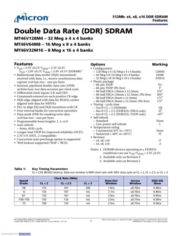
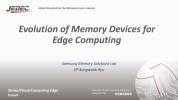
Technology Double Data Rate (DDR) Memories– Memory transfer upon rising and falling edgesof the clock signal permits double the transfer rate withoutincreasing the frequency of the clock signal– Advanced error correction features can beemployed– Cell disturbance via Rowhammer hasmanifested in DDR3 & DDR4 due to featurescaling– Typical software model: Flight computers boot from ROM, but tend torun from RAM RAM permits larger data sets to be processedconcurrently Memory array does not have to be DRAMWe are focusing on a DDR interfacePresented by Edward J. Wyrwas at the 2018 NEPP Electronics Technology Workshop (ETW), NASA GSFC, Greenbelt, MD, June 18-21, 2018.4
FY18-19: DDR TestingDescription:FY18-19 Plans:– This is a task over all device topologies and process.– Prove out DDR4 test capability– The intent is to determine inherent radiation tolerance andsensitivities,– Identify challenges for future radiation hardening efforts,– Investigate new failure modes and effects– Testing includes total dose, single event (proton) and reliability.Test vehicles will include a variety of volatile memory devicesas available– Probable test structures for TID and SEE:– Micron– Samsung– Hynix– Nanya– Intelligent Memory– Tests:– characterization pre and n-going discussions for test samplesDDR4 Tester DevelopmentFY18MJJT ID T estingSEE TestingAnalysis and ComparisonASONFY19D JF MA– Test reports and quarterly reports– Expected submissions for publicationsNASA and Non-NASA Organizations/Procurements:– Source procurements: TID (GSFC), Proton (MGH, Cincy,NWMCPC, Mayo, Provision)Lead Center/PI: GSFC/Lentech/WyrwasPresented by Edward J. Wyrwas at the 2018 NEPP Electronics Technology Workshop (ETW), NASA GSFC, Greenbelt, MD, June 18-21, 2018.5
DDR RoadmapDDR2– ISSI– Hynix– Samsung– MicronRadiation TestingTBDReliability TestingDDR3– Intelligent Memories– Hynix– Samsung– Micron 16nmTBDRadiation TestingReliability TestingDDR4– Samsung– Micron– Hynix– Nanya– Intelligent MemoriesRadiation TestingReliability TestingDDR-like & 3D Memories– DiRAM (Tezzaron)– 3D Xpoint (Intel Optane)– Everspin MRAM DDR3FY11TBDRadiation TestingTBD---FY17FY18Presented by Edward J. Wyrwas at the 2018 NEPP Electronics Technology Workshop (ETW), NASA GSFC, Greenbelt, MD, June 18-21, 2018.FY196
Test Readiness– Collaboration with Kozio has yielded a straightforward economic approach to testing multiple DDR4 types and speed grades– Single and Dual Rank DIMMs– Single and multiple chip select (CS)– ECC and non-ECC– Based on a low cost reference design board (RDB) from NXP/Freescale– LS1046A-RDB containing four (4) 64-bit ARM Cortex-A72 microprocessors– DRAM Controller is 32 \ 64-bit DDR4– Software is loaded over the JTAG port using USB 2.0, but run from the microprocessor– Software permits a comprehensive test suite to produce and apply payload patterns to the DRAM– During benchmarking we are able to do 0s, 1s, checkerboard, inverted-checkerboard, ‘walking 1s’ and ‘walking 0s’ patterns with read, write, verify(RWV) in under 60 seconds– Software loads custom firmware for DDR4 controller during hardware initialization– We have established a relationship with a supplier to build socketed DDR4 DIMMs– for each available type of memory (both FBGA78 and FBGA96 chip components)– across our five (5) semiconductor vendors– Same configuration can be utilized with DDR3 memoryPresented by Edward J. Wyrwas at the 2018 NEPP Electronics Technology Workshop (ETW), NASA GSFC, Greenbelt, MD, June 18-21, 2018.7
Plans Moving Forward– We will be procuring DIMMs:–––––UDIMM, single-sided, 7 Chips plus 1 socket, all x8 in FBGA78UDIMM, double-sided, 15 Chips plus 1 socket, all x8 in FBGA78ECC UDIMM, single-sided, 8 Chips plus 1 socket, all x8 in FBGA78ECC UDIMM, double-sided, 17 Chips plus 1 socket, all x8 in FBGA78UDIMM, single-side, 3 Chips plus 1 socket, all x16 in FBGA96– The DIMMs will be assembled using DDR4 components gent Memories– The NXP LS1046A-RDB will receive an interposer to extend the DIMMabove the circuit board to permit better alignment to radiation sourcesPresented by Edward J. Wyrwas at the 2018 NEPP Electronics Technology Workshop (ETW), NASA GSFC, Greenbelt, MD, June 18-21, 2018.8
Comments– Sad News:– Kozio is leaving the DDR calibration and testing business– But we have an arrangement to continue to use their code library to continue the development of our platform– We have ongoing collaboration with JPL, Kozio, Cubic Aerospace, Everspin (MRAM), and others– Please contact Ed if you have any interest in DDR memory devices– Emerging non-volatile memory (NVM) technologies are beginning to infiltrate the computing regime as storage-classmemory (SCM)– SCM uses NVM as the storage and DRAM as a cache for active data– Some NVM technologies can be tested as DDRParadigmShiftImage from white paper: Intel Optane SSDs with Intel Memory Drive Technology, 2018 , 334784-003USPresented by Edward J. Wyrwas at the 2018 NEPP Electronics Technology Workshop (ETW), NASA GSFC, Greenbelt, MD, June 18-21, 2018.9
Double Data Rate (DDR) Memory Devices Presented by Edward J. Wyrwas at the 2018 NEPP Electronics Technology Workshop (ETW), NASA GSFC, Greenbelt, MD, June 1821, 2018-. 1 Acknowledgment: This work was sponsored by: NASA Electronic Parts and Packaging (NEPP) Edward J. Wyrwas edward.j.wyrwas@nasa.gov 301-286-5213 Lentech, Inc. in support of NEPP
