Transcription
DHAN-T ModuleDECT ULE PlatformDatasheetVersion 2.6July 2021
Version 2.6DHAN-T DECT ULE ModuleDisclaimerThis document is provided by DSP Group, Inc. and/or one or more of its subsidiaries (“DSP Group”). All information and datacontained in this document is for informational purposes only, without any commitment on the part of DSP Group, and is not tobe considered as an offer for a contract. DSP Group shall not be liable, in any event, for any claims for damages or any otherremedy in any jurisdiction whatsoever, whether in an action in contract, tort (including negligence and strict liability) or any othertheory of liability, whether in law or equity including, without limitation, claims for damages or any other remedy in whateverjurisdiction, and shall not assume responsibility for patent infringements or other rights to third parties, arising out of or inconnection with this document. Further, DSP Group reserves the right to revise this publication and to make changes to its content,at any time, without obligation to notify any person or entity of such revision changes. These materials are copyrighted and anyunauthorized use of these materials may violate copyright, trademark, and other laws. Therefore, no part of this publication maybe reproduced, photocopied, stored on a retrieval system, or transmitted without the express written consent of DSP Group. Anynew issue of this document invalidates previous issues.DSP Group reserves the right to revise this publication and to make changes to its content, at any time, without obligation to notifyany person or entity of such revision changes. 2021 DSP Group Confidential. All rights reserved.For DSP Group worldwide sites and related contact information, see http://www.dspg.com/corporate/officesJuly 2021DSP Group Confidential2/19
Version 2.6DHAN-T DECT ULE ModuleTable of ContentsTABLE OF CONTENTS1INTRODUCTION . 41.11.21.3General Description . 4Features. 4Block Diagram . 42PIN AND SIGNAL DESCRIPTION . 53ELECTRICAL SPECIFICATIONS . 83.13.23.33.43.5Absolute Maximum Ratings . 8Recommended Operating Conditions . 8Peak and Hibernation Currents . 8Transmitter. 9Receiver . 94APPLICATION REFERENCE SCHEMATIC . 105INTERFACING DHAN-T WITH EXTERNAL MCU . 115.15.2RSTN Input. 11UART, SPI Interfaces . 116APPLICATION PCB DESIGN RECOMMENDATIONS . 127ASSEMBLY INFORMATION . 137.17.27.38Mechanical Drawing . 13PCB Footprint Detail . 13Pick & Place, Reflow . 14SUPPLEMENTARY INFORMATION . 158.18.28.38.48.58.68.7July 2021Labeling . 15Handling Guidance . 15FCC and IC Interference Statement . 16Declaration of Conformance (DoC). 16IPEI and EMC . 16Ordering Information . 17Change Log. 17DSP Group Confidential3/19
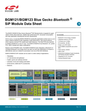
Version 2.6DHAN-T DECT ULE ModuleIntroduction1 Introduction1.1 General DescriptionDSP Group’s DHAN-T module is based on the state-of-the-art DHX101, a 4th generation DECT System on aChip (SoC). The DHAN-T module is well suited for all DECT and ULE device applications. The DHAN-Tsoftware stack includes standard DECT ULE MAC-PHY connectivity as well as HAN-FUN (ULE Alliancestandard) functionality for Dual-Mode (data and audio) ULE. The application software written by the customertypically runs atop the communication stack running on the DHX101 within the DHAN-T. However, theapplication Host can also run on an external MCU that communicates with the DHAN-T via a UART interface.1.2 Features Excellent radio performance, with over 119dB system gain Includes a printed antenna Radio covers all regional DECT bands with a simple re-configuration of the EEPROM Fully compliant with ETSI DECT and ULE standards, awarded CE, FCC and IC certification Compact dimensions: 27.2x16.9x3.3mm (including the RF shield height) Minimized external BOM Operating temperature: -40ºC to 85ºC1.3 Block ing/FilterI2C, UART, SPI, JTAG, TDM32.768K32.768KFigure 1-1: DHX101 DHAN-T Module Block DiagramJuly 21, 2021DSP Group Confidential4/19
Version 2.6DHAN-T DECT ULE ModulePin and Signal Description2 Pin and Signal DescriptionSee Figure 2-1 and Table 2-1 for detailed pin diagram and description.Figure 2-1: DHAN-T Module Pin DiagramTable 2-1: DHAN-T Module Pin DescriptionJuly 21, 2021PIN NO.NAME1GNDGND2ANTDiversity antenna. Leave not connected (NC)3RSTN4DCINSDESCRIPTION/TYPEFor standalone operation, shunt this pin to GND with100nF. For an application running on an externalMCU, this pin should be connected to a Host MCUIO and used to reset the DHAN-TLeave NCDSP Group Confidential5/19
Version 2.6July 21, 2021DHAN-T DECT ULE ModulePin and Signal DescriptionPIN NO.NAMEDESCRIPTION/TYPE5GPIO176SCL (GPIO0)GPIO or I2C Clock. Open Drain, reset value isfloating. Leave NC if not used.7SDA (GPIO1)GPIO or I2C Data. Open Drain, reset value isfloating. Leave NC if not used.8GPIO2GPIO or TDM TXD9GPI03GPIO or TDM RXD10GPIO4GPIO or TDM FSYNC11GPIO5GPIO or TDM FSYNC12GPIO6GPIO or SPI Data In. Leave NC if not used13GPIO7GPIO or SPI Data Out. Leave NC if not used14GPIO8GPIO or SPI Clock15GPIO9GPIO or UART Rx or SPI Chip Select16VCC GPIO17USB DM18USB DP19TDIJTAG Data In. Connect to TP20TDOJTAG Data Out. Connect to TP21GND22TMSJTAG Mode Select. Connect to TP23TCKJTAG Clock. Connect to TP24RTCKJTAG Reset. Connect to TP25GPIO10GPIO or UART 5LEDSINK2/DCIN136GNDInput. Sets the IO Logic level at the moduleinterface at 1.8 or 3V.3V (Doubler) Output. While DHAN-T ishibernating, this pin is either in tristate (default SWconfiguration) or pulled to GND. Can be used inconjunction with GPIO7 and 8 above to drive aLED or button during non-hibernation modesPull down with 1M resistorULE I/O. Leave NC if not usedGNDDSP Group Confidential6/19
Version 2.6July 21, 2021DHAN-T DECT ULE ModulePin and Signal DescriptionPIN NO.NAMEDESCRIPTION/TYPE37LEDSINK1/PWM38DCIN339AMP2 OUTULE I/O. Typically used (as input) to wake up theDHAN-T from hibernation40AMP1 OUTULE I/O. Typically used (as output) to indicateDHAN-T is active (logic high)41ANA2 IN42MPWR43MINLeave NC if not used44MIPLeave NC if not used45ANA IN1ULE I/O. Leave NC if not used46SPOUTPSpeaker Output, Positive47SPOUTNSpeaker Output, Negative48HSSPOTPHeadset Speaker Out, Positive49LOUTHeadset Speaker Out, Negative50PWM0Analog Output51XIN 32KConnect to 32.768 XTAL52XOUT 32KConnect to 32.768 XTAL53VDD ULE1.8V output. Active during hibernate. Can be usedto power VCC GPIO (Pin16)54VDD APU1.8V Test Point. Leave NC55VBATPower Supply Input. Connect to battery or regulated3V supply56GNDGNDADC input used to monitor power supply inputULE I/O. During hibernate, Logic High should notbe applied to this pin (it can result in leakagecurrent). Leave NC if not usedMicrophone PowerDSP Group Confidential7/19
Version 2.6DHAN-T DECT ULE ModuleElectrical Specifications3 Electrical SpecificationsUnless otherwise noted, all specifications are for 25ºC.3.1 Absolute Maximum RatingsMinimum voltage applied to all pins: -0.3VMaximum voltage applied to all pins: 4.6VStorage temperature range: -45 to 90ºCNote: Functionality at or above these limits is not implied. Exposure to absolute maximum ratings for extendedperiods may affect device reliability.3.2 Recommended Operating ConditionsTable 3-1: Recommended Operating ConditionsRATINGOperating ambienttemperatureVBATCONDITIONSAll GPIOsCondition:VCC GPIO is 3VVILVIHVOLVOHAll GPIOsCondition:VCC GPIO is1.8VVILVIHVOLVOHRSTNVILVIHDCIN3MINTYPMAXUNIT-40 25 85 VVBATV0.6*VBAT1.953.03.3 Peak and Hibernation CurrentsVBAT 3VTable 3-2: Peak and Hibernation CurrentsPARAMETERJuly 21, 2021TEST CONDITIONSTYPMAXUNITTx CurrentBand EU @ 23dBm400480mATx CurrentBand US @ 21dBm250300mARx CurrentMax Gain Setting125135mADSP Group Confidential8/19
Version 2.6DHAN-T DECT ULE ModulePARAMETERTEST CONDITIONSPaging CurrentElectrical SpecificationsTYP1s response latencyMAXUNIT90µA2µAHibernationCurrent3.4 TransmitterVBAT 3VTable 3-3: Tx CharacteristicsTEST CONDITIONSMINTYPMAXNTPCHARACTERISTICSBand EU21.52324dBmUNITNTPBand US192021dBmHarmonicsBand EU & US-40-35dBmTransmission MaskEN 301406Paragraph 5.3.3ComplyFrequency OffsetEN 301406Paragraph 5.3.1-508 50KHzFrequency DriftEN 301406Paragraph 5.3.5-150 15KHz/SlotEmission DueModulationEN 301406Paragraph 5.3.6.2M 1M 2M 3M 3N/AdBm-20-42-47-50-8-30-40-443.5 ReceiverVBAT 3VTable 3-4: Rx CharacteristicsCHARACTERISTICSJuly 21, 2021TEST CONDITIONSSensitivity, BER 1000ppmEU BandMaximum input powerEU BandDSP Group ConfidentialMINTYPMAXUNIT-96-93dBm15dBm9/19
Version 2.6DHAN-T DECT ULE ModuleApplication Reference Schematic4 Application Reference SchematicFigure 4-1: DHAN-T Reference SchematicJuly 21, 2021DSP Group Confidential10/19
Version 2.6DHAN-T DECT ULE ModuleInterfacing DHAN-T with External MCU5 Interfacing DHAN-T with External MCU5.1 RSTN InputAt power-up, the Application Host on the external MCU should hold pin 3 (RSTN Input) at logic Low until itis ready to establish communication (via UART) with the DHAN-T. When ready, the Application Host shouldapply a rising edge (and leave at Logic High) and wait for the “Hello” indication from the DHAN-T. If at somepoint later on the MCU cannot communicate with the DHAN-T, it should apply a low going pulse of 100uSto reset the DHX101 on the DHAN-T. Note that the RSTN pin is powered by the VBAT power domain. Theminimum Logic High level is 0.6*VBAT.5.2 UART, SPI InterfacesApplications requiring a UART I/F and an SPI interface (eg, SmartVoice ULE applications), map the former toGPIOs 10 and 11 (Rx, Tx respectively) and the latter to GPIOs 6-9. Where only the UART I/F is required (asin the Reference Schematic provided in section 4), UART Rx is assigned to GPIO9 and Tx to GPIO10.July 21, 2021DSP Group Confidential11/19
Version 2.6DHAN-T DECT ULE ModuleApplication PCB Design Recommendations6 Application PCB Design RecommendationsIt is recommended that unused pads on the Application PCB not be left as isolated islands of copper but ratherbe anchored via inner layers of the PCB. It is also recommended that GND vias be applied liberally in thevicinity of GND pins 1, 21, 36 and 56.The following layout recommendations for embedding the DHAN-T on the Application board:1. Implement a solid ground under the DHAN-T module.2.Do not route signal traces under the module. Use the bottom layer for signal routing.3.Locate the module such that the printed antenna overhangs to application PCB (refer to photo below)4.Release from GND on all layers under the DHAN-T antenna.Figure 6-1: Placement of ModuleJuly 21, 2021DSP Group Confidential12/19
Version 2.6DHAN-T DECT ULE ModuleAssembly Information7 Assembly Information7.1 Mechanical Drawing /-10%15.3mm /- 1mmShield Width7.2 PCB Footprint DetailJuly 21, 2021DSP Group Confidential13/19
Version 2.6DHAN-T DECT ULE ModuleAssembly Information7.3 Pick & Place, ReflowThe DHAN-T module uses a flat shield cover to facilitate a fully automatic assembly process. For backing andreflow recommendations, use MSL 3 in the JEDEC/IPC standard J-STD-20b. The temperature classification(TC) for the module is 245 C.July 21, 2021DSP Group Confidential14/19
Version 2.6DHAN-T DECT ULE ModuleSupplementary Information8 Supplementary Information8.1 LabelingSee Figure 8-1 for labeling details. The label is attached to the module shield.Figure 8-1: DHAN-T Module Labeling Details8.2 Handling GuidanceThis module includes highly sensitive electronic circuity. Handling without proper ESD protection may damagethe module permanently.July 21, 2021DSP Group Confidential15/19
Version 2.6DHAN-T DECT ULE ModuleSupplementary Information8.3 FCC and IC Interference StatementThis device complies with part 15 of the FCC rules and RSS-247 of Industry Canada. Operation is subject tothe following two conditions: (1) this device may not cause harmful interference, and (2) this device must acceptany interference received, including interference that may cause undesired operation.Le présent appareil est conforme aux CNR d'Industrie Canada applicables aux appareils radio exempts delicence. L'exploitation est autorisée aux deux conditions suivantes : (1) l'appareil ne doit pas produire debrouillage, et (2) l'utilisateur de l'appareil doit accepter tout brouillage radioélectrique subi, même si lebrouillage est susceptible d'en compromettre le fonctionnement.This Class B digital apparatus complies with Canadian ICES-003.Cet appareil numérique de la classe B est conforme à la norme NMB-003 du Canada.NOTE: The manufacturer is not responsible for any radio or TV interference caused by unauthorizedmodifications to this equipment. Such modifications could void the user’s authority to operate the equipment.NOTE: This equipment has been tested and found to comply with the limits for a Class B digital device,pursuant to part 15 of the FCC Rules. These limits are designed to provide reasonable protection againstharmful interference in a residential installation. This equipment generates uses and can radiate radio frequencyenergy and, if not installed and used in accordance with the instructions, may cause harmful interference toradio communications. However, there is no guarantee that interference will not occur in a particularinstallation. If this equipment does cause harmful interference to radio or television reception, which can bedetermined by turning the equipment off and on, the user is encouraged to try to correct the interference by oneor more of the following measures: Reorient or relocate the receiving antenna. Increase the separation between the equipment and receiver. Connect the equipment into an outlet on a circuit different from that to which the receiver is connected. Consult the dealer or an experienced radio/TV technician for help This device and its antenna(s) must not be co-located or operating in conjunction with any other antenna ortransmitter8.4 Declaration of Conformance (DoC)DSP Group declares that the radio equipment type DHAN-T is in compliance with Directive 2014/53/EU.The full text of the EU Declaration of Conformity is available at the Internet address www.dspg.com.8.5 IPEI and EMCEach DHAN-T nodule is shipped to the customer with a unique IPEI, which serves as its DECT identity.DHAN-T will ship with an “EMC” of 0xFEB. This is the DSP Group “generic” EMC. The EMC settingidentifies a Device as belonging to a specific group of ULE Devices/Hubs that utilize some proprietarysignaling.In either case, the customer is free to re-program these parameters.July 21, 2021DSP Group Confidential16/19
Version 2.6DHAN-T DECT ULE ModuleSupplementary Information8.6 Ordering InformationPart #: DHX101MDMDFDB0AMI8.7 Change LogTable 8-1: List of ChangesREVISIONDATEDESCRIPTION1.1June 4, 20181.2August 8,2018Updated PCB files2.0May 27,2019*Account for migration to DHX101, FW D (Part #, Block Diagram, pagingidle current drain)*Clarifications to, VCC IO RSTN (pinout description, drive by externalMCU)*Clarifications to TDM, SPI mapping to GPIO*Added Reference Schematics2.1June 3, 20192.2April 16,20202.3January 13,20212.4March 4,2021*Added battery input to ADC in reference schematic*Noted that module was awarded regulatory certification2.5April 6,2021*Updated document styles and numberingBaseline release*Added detail PCB footprint drawing*Clarified in Module Description that dimensions given are for the moduleitself, not the PCB footprint recommended for mounting the module*Replaced pinout diagram with more legible pin labels*Corrected JTAG TDO and TMS pin numbering in the tabulation. Nowmatches the diagram*Added labeling description*Added tolerances to shield height and PCB thickness dimensions*Added FCC & IC Interference Statement, Declaration of Conformance(DoC)*Updated part #*Added List of Figures and List of Tables2.6July 21, 2021July 21,2021*Section 6. Clarify module placement and antenna overhang on theapplication PCBDSP Group Confidential17/19
Version 2.6DHAN-T DECT ULE ModuleList of FiguresLIST OF FIGURESFigure 1-1: DHX101 DHAN-T Module Block Diagram . 4Figure 2-1: DHAN-T Module Pin Diagram . 5Figure 4-1: DHAN-T Reference Schematic . 10Figure 6-1: Application PCB Design . 12Figure 8-1: DHAN-T Module Labeling Details . 15July 21, 2021DSP Group Confidential18/19
Version 2.6DHAN-T DECT ULE ModuleList of TablesLIST OF TABLESTable 2-1: DHAN-T Module Pin Description . 5Table 3-1: Recommended Operating Conditions . 8Table 3-2: Peak and Hibernation Currents . 8Table 3-3: Tx Characteristics . 9Table 3-4: Rx Characteristics . 9Table 8-1: List of Changes . 17July 21, 2021DSP Group Confidential19/19
to reset the DHX101 on the DHAN-T. Note that the RSTN pin is powered by the VBAT power domain. The minimum Logic High level is 0.6*VBAT. 5.2 UART, SPI Interfaces Applications requiring a UART I/F and an SPI interface (eg, SmartVoice ULE applications), map the former to GPIOs 10 and 11 (Rx, Tx respectively) and the latter to GPIOs 6-9.