Transcription
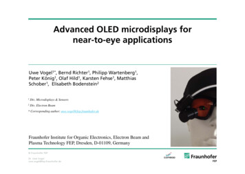
Advanced OLED microdisplays fornear-to-eye applicationsUwe Vogel1*, Bernd Richter1, Philipp Wartenberg1,Peter König1, Olaf Hild1, Karsten Fehse1, MatthiasSchober1, Elisabeth Bodenstein21Div. Microdisplays & Sensors2Div. Electron Beam* Corresponding author: uwe.vogel@fep.fraunhofer.deFraunhofer Institute for Organic Electronics, Electron Beam andPlasma Technology FEP, Dresden, D-01109, Germany Fraunhofer FEPDr. Uwe Vogeluwe.vogel@fep.fraunhofer.de
Fraunhofer FEP Fraunhofer FEPDr. Uwe Vogeluwe.vogel@fep.fraunhofer.de
Fraunhofer FEP Core Competencies Fraunhofer FEPDr. Uwe Vogeluwe.vogel@fep.fraunhofer.deELECTRON BEAMTECHNOLOGYPLASMA-ACTIVATEDHIGH-RATE DEPOSITIONSPUTTERINGTECHNOLOGYHIGH-RATE PECVDTECHNOLOGIES FORORGANIC ELECTRONICSIC ANDSYSTEM DESIGN
Introduction: The case for OLED microdisplays in NTE OLED-on-Silicon technology Highly efficient light source and imager in one(emissive microdisplay) Low-power High contrast No backlight-related virtualscreen for see-through (ST) Smallest system footprint high-resolution & -accuracy patterning Pixel pattern determined by CMOSphotolithography OLED pixel density 1,000.5,000.10,000ppi arbitrary emission shapes fast response time (MHz) electronics feature integration driving, control, processing CMOS sensor co-integration andacquisition Fraunhofer FEPDr. Uwe Vogeluwe.vogel@fep.fraunhofer.de
Introduction: Microdisplay challenges in ST-NTE applications Sun-light conditions high-brightness ( 5,000 cd/m²) Lifetime regularly accompanied by elevatedtemperature operation lowest pixel pitch, directly correlatingto die size and cost Limited by voltage driverequirements for high-brightness(OLED LIV) low-power operation for long batterylife, affected by OLED efficiency andbackplane architecture, extended color gamut, embedded modes for user interaction,e.g., embedded sensors andemission/detection outside the visible. Fraunhofer FEPDr. Uwe Vogeluwe.vogel@fep.fraunhofer.de
OLED microdisplay challenges How to address those challenges? OLED micro-patterning Electron-beam direct-writing Embedded sensors, spectral characteristics Bi-directional OLED microdisplay Backplane architecture DRAM vs. SRAM Fraunhofer FEPDr. Uwe Vogeluwe.vogel@fep.fraunhofer.de
OLED microdisplay challenges How to address those challenges? OLED micro-patterning Electron-beam direct-writing Embedded sensors, spectral characteristics Bi-directional OLED microdisplay NIR/UV emission Backplane architecture DRAM vs. SRAM Fraunhofer FEPDr. Uwe Vogeluwe.vogel@fep.fraunhofer.de
State-of-the-art OLED display color-patterning technologiesWhite OLED with color-filter (CF)EML patterning by shadow maskingencapsulationCF RedCF GreencathodeETLencapsulationCF BluecathodeETLW-EMLAnode R HTLAnode GCMOS WaferAnode BSimple processHomogeneous alterationLow efficiencyColor diffusionAll commercial OLED microdisplays asof today Fraunhofer FEPDr. Uwe Vogeluwe.vogel@fep.fraunhofer.de R-EMLG-EMLB-EMLAnode RHTLAnode GCMOS WaferAnode BWide color gamutHigh contrastLow resolution ( 600ppi as of today)Limited scaleabilityDifferential aging
Comparison of OLED patterning ine metal masking30 µmSmall-molecules onlySamsungVapor Jet40 µmSmall-molecules onlyUDCLIFT3 µmSmall-molecules onlySamsung / 3MLITI40 µmSmall-molecules and polymersSamsung / 3MImprint Lithography 10 nmmoldable resists, functional organicsXCapillary molding50 nmresists, low-viscosity inks, functionalorganicsXSoft Printing 0.1-2 µmSAM, thin metals, org. & anorg.semiconductorsXInkjet Printing 10-20 µmSmall-molecules and polymersPanasonicFlash-mask transferlithography 10 µmSmall-molecules onlyPhotolithography 1 µmResists, functional organicsFraunhofer FEPElectron-beam direct write 1 µmOrganics and inorganicsFraunhofer FEP Fraunhofer FEPDr. Uwe Vogeluwe.vogel@fep.fraunhofer.deVon Ardenne
OLED emission modification by electron-beam (EB) direct-write Goal: high-res (1.10µm) EB-induced EML/OLED patterning Achieved so far: Emission of OLED can be individually modified byEB process after encapsulation penetrating electrons of EB leads to localreduction in charge carrier injection,which permanently reduces the localemission levelElectron energy dose electron dose defines degree of dimming reduced local emission conductivity Electron energy determines theirpenetration depth into the OLED layer stack500 µm Energy can be deposited in layers underneath the encapsulationlayers without destroying the encapsulation itself Individual organic layers can be directly targeted Fraunhofer FEPDr. Uwe Vogeluwe.vogel@fep.fraunhofer.de
Simulation of electron energy absorbed in OLED layer stack Estimation of penetration depth and energy absorption of the electrons in the OLEDstack by Monte Carlo simulations specific layer properties and scattering processesat interfaces must be taken into account Majority of the energy is absorbed inthe encapsulation layers and only afraction reaches the delicate organiclayers Fraunhofer FEPDr. Uwe Vogeluwe.vogel@fep.fraunhofer.de
High-resolution patterning by electron-beam direct-write Lateral control of theelectron beam and pixelby-pixel adjustment of thegrey-value enables highresolution direct-writepatterning Design example: Picture ofSemperoper Dresden Image size: 1,8 x 1,2 mm2 Resolution: 2 μm / 12.700ppi Writing time: 105 s Fraunhofer FEPDr. Uwe Vogeluwe.vogel@fep.fraunhofer.deElectron Beam patterning in cooperation with Raith GmbH
High-resolution patterning by electron beam direct-write Application examples: Signage - Micro and miniature displays, large-areacustom-designed lighting components, emissivetattoos / eSkinIntegrated security features (PUFs – physicallyunclonable functions) - emissive passport photos Fraunhofer FEPDr. Uwe Vogeluwe.vogel@fep.fraunhofer.de Emissive measuring devicessuch as rulers and yardsticks Data Storage applications
OLED microdisplay challenges How to address those challenges? OLED micro-patterning Electron-beam direct-writing Embedded sensors, spectral characteristics Bi-directional OLED microdisplay Backplane architecture DRAM vs. SRAM Fraunhofer FEPDr. Uwe Vogeluwe.vogel@fep.fraunhofer.de
Bi-directional OLED microdisplaySVGASVGA Fraunhofer FEPDr. Uwe Vogeluwe.vogel@fep.fraunhofer.de
Bi-directional OLED-on-silicon microdisplays no imaging optics so far Fraunhofer FEPDr. Uwe Vogeluwe.vogel@fep.fraunhofer.de- Confidential -16
Bi-directional OLED-on-silicon microdisplays Feedback-mode demonstrator no imaging optics so far Fraunhofer FEPDr. Uwe Vogeluwe.vogel@fep.fraunhofer.de- Confidential -17
Bi-directional OLED microdisplay Adds eye/gaze-controlled (i.e.,hands/voice-free) interactivity tosmart glasses Enables vergence monitoringLine-of-sight Fraunhofer FEPDr. Uwe Vogeluwe.vogel@fep.fraunhofer.de
21Bi-directional OLED microdisplays for eye-controlled interactive smart glasses Glass@Service: „Interactive personalized visualization in industrial processes as part of DigitalFactory in electronics manufacturing“ Funded within „Smart Service World“ of BMWi, started Mar‘16 Fraunhofer FEPDr. Uwe Vogeluwe.vogel@fep.fraunhofer.de
OLED microdisplay challenges How to address those challenges? OLED micro-patterning Orthogonal photolithography Electron-beam direct-writing Embedded sensors, spectral characteristics Bi-directional OLED microdisplay NIR/UV emission Backplane architecture DRAM vs. SRAM Fraunhofer FEPDr. Uwe Vogeluwe.vogel@fep.fraunhofer.de
Microdisplay Backplane Architecture For NTE long battery life often moreimportant than frame rate/resolution display simple graphics (e.g., symbols)and text alteration frequency of screen contentlow ( 5Hz) image data stored in a static randomaccess memory SRAM-like pixel cellarchitecture Direct serial pixel-wise addressingscheme enables much lowerbandwidth for display interface strong reduction of display power byminimizing backplane consumption OLED power/efficiency determinesoverall power consumption now Even VIDEO power advantage formoderate frame rates and resolution Fraunhofer FEPDr. Uwe Vogeluwe.vogel@fep.fraunhofer.de
Microdisplay Power ConsumptionBidirectional OLED microdisplay:- 0,6“ 800 x 600, 16μm pixel pitch- full color @ 200nits- with embedded image sensor200mWdisplay powerfull screen on3mW Fraunhofer FEPDr. Uwe Vogeluwe.vogel@fep.fraunhofer.deUltra-low-power microdisplay:- 0.2“ 304 x 256, 12um pixel pitch- monochrome green @ 600nits
Conclusion & Outlook27 Challenges for OLED microdisplays in near-to-eye applications Full-color high-brightness, High-temperature, Lifetime, Minimum pixel pitch,Low-power consumption, long battery life, Wide color gamut, User Interaction Approaches to address OLED micro-patterning Photolithography Lift-off: general yield issues (Dry) Etching: under evaluation Electron-beam direct-writing Fixed images at 2μm shown micro-signage R,G,B-subpattering under evaluation Embedded sensors, extended spectral characteristics Bi-directional OLED microdisplay gaze-interactivity for NTE NIR/UV emission non-VIS NTE; fluorescence sensors, optogenetics Backplane architecture SRAM for low-power NTE Fraunhofer FEPDr. Uwe Vogeluwe.vogel@fep.fraunhofer.de
SID Mid-Europe Chapter Spring Meeting 2017 http://www.fep.fraunhofer.de/sidme17 Program Committee/Key notes: ZEISS Intel Microsoft Microoled Kopin Sony Volkswagen Univ. of Cambridge Univ. of Edinburgh Fraunhofer FEPDr. Uwe Vogeluwe.vogel@fep.fraunhofer.de28
Contact Dr. Uwe Vogel Head of Division OLED Microdisplays and Sensors Deputy Director Fraunhofer Institute for Organic Electronics, Electron Beam and Plasma Technology FEP Maria-Reiche-Strasse 2D-01109 Dresdenphone: 49-351-8823-282email: uwe.vogel@fep.fraunhofer.de Acknowledgements Dr. Alexander Zakhidov, Texas State University Work was in parts sponsored by European Commission within the HYPOLED project (High-Performance OLED-Microdisplays for Mobile Multimedia HMD and ProjectionApplications, ICT-2007.3.2-217067) Federal Ministry for Education and Research of the German government (Bundesministerium für Bildung und Forschung), BMBF 01 BK916-919, 16SV2283/"ZOOM", 16SV3682/"ISEMO“, 16SV5036 “NIR-OLED” Sächsische Aufbaubank (SAB) of the State of Saxony (11107/1733 “A18HVMOS” & 100070897 “Cool Projector”) Fraunhofer Internal Programs “iSTAR” Grant No. WISA 817 805, “3D Signage” Grant No. MAVO 823279, “OLITH” Grant No. ATTRACT162-600032 Fraunhofer FEPDr. Uwe Vogeluwe.vogel@fep.fraunhofer.de29
High-resolution patterning by electron-beam direct-write Lateral control of the electron beam and pixel-by-pixel adjustment of the grey-value enables high-resolution direct-write patterning Design example: Picture of Semperoper Dresden Image size: 1,8 x 1,2 mm2 Resolution: 2 μm / 12.700 ppi Writing time: 105 s
