Transcription
protocolSoft lithography for micro- and nanoscalepatterningDong Qin1, Younan Xia2 & George M Whitesides3Nano Research Facility and Department of Energy, Environmental, and Chemical Engineering and 2Department of Biomedical Engineering, Washington University,St. Louis, Missouri, USA. 3Department of Chemistry and Chemical Biology, Harvard University, Cambridge, Massachusetts, USA. Correspondence should be addressedto G.M.W. (gmwhitesides@gmwgroup.harvard.edu).1 2010 Nature Publishing Group http://www.nature.com/natureprotocolsPublished online 18 February 2010; doi:10.1038/nprot.2009.234This protocol provides an introduction to soft lithography—a collection of techniques based on printing, molding and embossingwith an elastomeric stamp. Soft lithography provides access to three-dimensional and curved structures, tolerates a wide variety ofmaterials, generates well-defined and controllable surface chemistries, and is generally compatible with biological applications.It is also low in cost, experimentally convenient and has emerged as a technology useful for a number of applications that includecell biology, microfluidics, lab-on-a-chip, microelectromechanical systems and flexible electronics/photonics. As examples, herewe focus on three of the commonly used soft lithographic techniques: (i) microcontact printing of alkanethiols and proteins ongold-coated and glass substrates; (ii) replica molding for fabrication of microfluidic devices in poly(dimethyl siloxane), and ofnanostructures in polyurethane or epoxy; and (iii) solvent-assisted micromolding of nanostructures in poly(methyl methacrylate).INTRODUCTIONThe strategy of ‘smaller brings new capability’ has begun to changethe world of biotechnology as it has transformed microelectronics1.Successful applications of small systems include microarrays forhigh-speed DNA sequencing2, microfluidic devices for performing PCR3, lab-on-a-chip (LOC) systems for synthesis and analysisof peptide and oligonucleotide libraries4, and microchips for drugscreening5 and for investigation of cultured cells6. As the workhorseof microfabrication, photolithography7 has contributed an important role in most of these applications, including the fabricationof DNA arrays in the late 1980s (ref. 8). However, this techniquehas a number of limitations for applications related to biologicalsystems. First, photolithography is an intrinsically expensive processbecause the equipment used was developed for the highly demanding processes required for fabrication of microelectronic devices.The capital investment required to build a clean room makesphoto lithography less than accessible to most chemists, biochemists and biologists. Thus, photolithography is most successful whenapplied to a limited set of materials. Users wishing to study ‘dirty’organic systems are usually excluded from an electronics-qualifiedclean-room facility. Second, photolithography is often carried outby projecting a pattern on a photomask onto a photoresist film.Although photomasks are commercially available, the time andcost involved in the fabrication of such masks present a signi ficant barrier to the use of photolithography in rapid, inexpensiveproto typing of test patterns and devices. Third, photolithographyprovides little or no control over surface chemistry, and it is notapplicable to curved or non-planar substrates.Soft lithography9 represents a conceptually different approach torapid prototyping of various types of both microscale and nanoscale structures, and devices on planar, curved, flexible and softsubstrates especially when low cost is required. A large numberof patterning techniques—microcontact printing (µCP)10, replicamolding (REM)11, microtransfer molding12, micromolding incapillary13, solvent-assisted micromolding (SAMIM)14, phaseshifting edge lithography15, nanotransfer printing16, decal transferlithography17 and nanoskiving18—form the basis of soft lithography; they are essentially based on printing, molding and embossingwith an elastomeric stamp (Protocols for µCP, REM and SAMIMare described in the Procedure and outlined in Fig. 1). New variantssuch as dip-pen nanolithography have also emerged19–21. All thesetechniques use organic and polymeric materials that are referredto as soft matter by physicists.µCPAs the forerunner of soft lithography, µCP provides an attractiveroute to microscale patterns and structures needed for applicationsin biotechnology. For example, µCP offers an ability to engineerthe properties of a surface with molecular-level detail using selfassembled monolayers (SAMs) of alkanethiols on a substrate coatedwith a metal such as gold (Au), silver (Ag), copper (Cu), palladium(Pd) and platinum (Pt)22. In this study, the substrate refers to aphysical object, which is somewhat different from the meaning inenzymology. Typical planar substrates for forming alkanethiolateSAMs include thin films of a metal deposited on silicon, mica, glassor even plastic materials. The substrates can be easily prepared byphysical vapor deposition methods, such as thermal or electronbeam evaporation23. The patterned SAMs have proved valuable forstudying the role of spatial signaling in cell biology by exquisitelycontrolling the molecular structure of a surface in contact withcells24. One can create well-defined regions with ‘cell-friendly’ (proteincovered) and ‘cell-unfriendly’ (polyethylene glycol–terminated) SAMsto pattern endothelial cells on a surface and then examine how thecells respond to lateral confinement, and to being released fromconfinement24. Furthermore, µCP has been successfully used to printprecise patterns of axon guidance mole cules, which can then serveas templates for growing chick retinal ganglion cell axons25.REMAlternatively, REM provides a new method for fabricating microfluidic devices using poly(dimethyl siloxane) (PDMS)26, and thismethod has proved to be particularly suitable for various biomedical applications27–32. Compared with the inorganic materialssuch as silicon and glass that are used in microelectronics andoptics, and which have been explored but largely discarded fornature protocols VOL.5 NO.3 2010 491
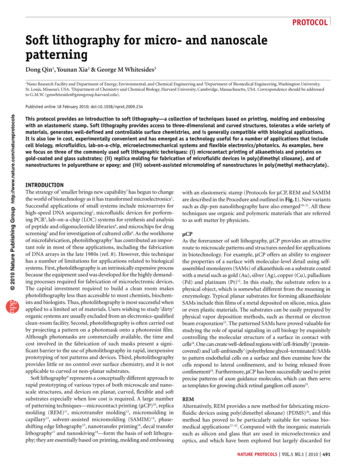
2010 Nature Publishing Group gically directed microfluidics, PDMS offers a number ofunique and attractive features. They are33: (i) It has a shear modulusof 0.25 MPa and a Young’s modulus of roughly 0.5 MPa (characteristic of a moderately stiff elastomer). This elastomeric characterallows it to conform to a surface and achieve atomic-level contact, afeature that is useful in forming and in sealing microfluidic systems.(ii) It is non-toxic and readily available from commercial sourcesat acceptable prices ( 80/kg). (iii) It is optically transparent downto about 300 nm. (iv) It is intrinsically hydrophobic (with a watercontact angle of 110 ), but its surface can be modified by briefexposure to an oxygen plasma to become hydrophilic (with a watercontact angle around 10 ). (v) It can adhere and seal reversibly or,after oxidation, irreversibly to many different types of substrates26,34.The ease of production associated with PDMS microfluidic structures will become even greater as the focus of microfluidics shiftsfrom demonstration of components and devices to developmentof fully functional systems31,35,36.Soft lithography also provides a set of attractive tools for nanofabrication. ‘Nanofabrication’ refers to a process that makes functional structures with at least one lateral dimension smaller than100 nm (ref. 37). REM and SAMIM are two techniques based onmolding or embossing with an elastomeric stamp. Both can produce nano scale structures in various soft materials, in parallel, overlarge areas (3 cm2 with 100-nm features), and at relatively low cost.When combined with selective etching and lift-off, these nanostructures have been transferred into metals and then used as substratesfor biosensing. The methods of detection have included opticaldiffraction38, surface plasmon resonance39, surface-enhancedRaman scattering40 and electrochemistry41.Photolithography versus soft lithographyPhotolithography will continue as the dominant technology in fabri cation of semiconductor devices and systems that have stringentrequirements on the alignment, continuity, isolation and uniformity in the final patterns. There are, however, many existing andemerging applications for soft lithography that take advantage of(or require) the characteristics of these techniques. For example,soft lithography offers access to a broader range of materials, aswell as experimental simplicity and flexibility in forming certaintypes of test patterns. Procedures involving relatively large features(such as those used in microfluidic devices) can be conducted inan ordinary chemical laboratory and are thus particularly usefulto those who do not have routine access to clean room facilities orfor applications where the fabrication cost is a serious concern. Atthe current stage of development, soft lithography still relies on theuse of photolithography to generate the master. Once the master isavailable, most of the fabrication tasks can be continued outside aclean room with the use of only a printing or molding procedure.As services for preparing the master are available from a numberof sites through the NSF-supported National NanotechnologyInfrastructure Network (NNIN), there is essentially no need tobuild and maintain a clean room facility before one can start toexplore the use of microscale structures, devices and systems.Experimental designFigure 1 outlines the four major steps of the procedure generallyused for soft lithography: (i) pattern design, (ii) fabrication of themask and then the master, (iii) fabrication of the PDMS stamp and(iv) fabrication of micro- and nanostructures with the stamp by492 VOL.5 NO.3 2010 nature protocolsI. Design of pattern(Steps 1 and 2)PhotomaskPositive resistII. Fabrication of master(Steps 3–6)Negative resistSubstrateSubstrateIII. Fabrication of PDMS stamp(Steps 6–11 or 12–19)PDMSPDMSIV. Soft lithography(Steps 20–46)Microcontact printing of SAM(Steps 20–25)Microcontact printing of protein(Steps 26–29)PDMSPDMSSiliconGlassSiliconGlassReplica molding of PU or epoxy(Steps 37–41)Solvent-assisted micro-molding of PMMA(Steps 42–47)PDMSPDMSPU or teFigure 1 Schematic illustration of the four major steps involved in softlithography and three major soft lithographic techniques.printing, molding and embossing. The term soft lithography ‘refersto the fabrication of patterned copies using the PDMS stamp’9;and the overall process—from pattern design to fabrication offunctional structures—is sometimes (when the convenience ofthe method for rapid generation of functional structures is thefeature emphasized) referred to as ‘rapid prototyping’42.Design of pattern. A number of computer-aided design (CAD)software programs are available to design a pattern. Adobe Freehandand Illustrator are two vector-based drawing programs well suitedfor quick design of a pattern with feature sizes down to 1 µm.These two software packages are widely accessible, easy to learn andparticularly useful for fabricating photomasks on transparencyfilms. Autodesk AutoCAD and DesignCAD are two advanced toolswith more capabilities such as higher precision and higher drawingspeed and are commonly used by a commercial supplier to designthe pattern on a chrome mask—a quartz (or fused silica) platepatterned with opaque chrome on its surface.Fabrication of mask. High-resolution printing provides a simpleand convenient method for fabricating photomasks on trans parency films42. The pattern created using Freehand or Illustratorand saved as an EPS file is compatible with most of the conventionalprinters or writers. Typically, a high-resolution commercial printer(5,060 d.p.i., with a dot size of 5 µm) can generate lines as thinas 20 µm and with acceptable edge resolution; this size range
2010 Nature Publishing Group http://www.nature.com/natureprotocolsprotocolis appropriate for most microfluidic applications. For higherresolutions down to 1 µm or submicron, chrome photomasks aretypically required.High-resolution printing service is available from the publication departments of universities or large companies, or from localcommercial printing shops. CAD/ART services in California offer20,000 d.p.i. printouts. The cost is substantially less expensive thanchrome masks. Chrome photomasks are available to be orderedfrom commercial suppliers such as Photo Sciences in the pricerange from hundreds to thousands of dollars depending on thefeature size and density of patterns on a photomask. For users inthe United States, services that prepare chrome masks are accessibleat a number of sites through the NSF-supported NNIN. For proofof concept and survey experiments, transparency masks are highlyrecommended to save cost and improve efficiency.PhotolithographySubstrateFabrication of elastomeric stamp. The key element of soft lithography is an elastomeric stamp with patterns as relief structures onits surface. The stamp is typically fabricated by casting a liquidprecursor against a master whose surface has been patterned withthe complementary structures. The mechanical properties of anelastomeric stamp are critical to its ability to transfer a patternwith high fidelity. In principle, any elastomer can be used to castthe stamp although most work has focused on the silicone-basedrubber or cross-linked PDMS. Among various types of commercial PDMS, Sylgard 184 from Dow Corning has been most commonly used for fabrication of stamps with feature sizes larger than500 nm. Composite stamps consisting of two layers—a stiff layer(30- to 40-µm-thick h-PDMS) supported by a flexible layer (3- to5-mm thick Sylgard 184 PDMS)—can extend the capability of softlitho graphy down to the 50–100 nm regime44. Figure 2 outlines aprocedure for fabricating Sylgard 184 and h-/184 PDMS compositeSubstrateSpin coat h-PDMSCast Sylgard 184SubstrateSylgard 184Cast Sylgard 184SubstrateSylgard 184CurePeel off from masterSylgard 184Fabrication of master. Photolithography and e-beam lithography(EBL) are the primary two techniques for fabricating a ‘master’ thatcontains patterned relief structures on the surface. However, otherrelief structures such as diffraction gratings and metal grids forelectron microscopy can also be useful for the fabrication of masters with certain simple patterns43. Conventional photolitho graphyis a classic technique for patterning structures with feature sizeslarger than 1 µm (ref. 7). Photolithography is often conducted in aclean room that is largely developed and used by the semiconductor industry to manufacture microelectronic chips. In academia, aclean room is usually located in a facility associated with an engineering program. Every user of a clean room needs to go throughan extensive training session before he/she can access the facility.The primary advantage of EBL over photolithography is its capacity to generate structures (20–30 nm in lateral dimensions) muchsmaller than those available through photolitho graphy (1–2 µm),which is mainly limited by optical diffraction (Cornell NanoScaleScience & Technology Facility). EBL starts from design andcreation of the desired pattern as a 2D vector graphics—that is,use of geometrical primitives such as points, lines, curves andpolygons to represent the pattern. As such, EBL is a serial process:it is generally much slower than photolithography, more expensive and subject to much longer waits for access to the facility. Ingeneral, EBL is a process that requires expensive equipment and anexperienced operator. For users in the United States, access to bothphotolithography and EBL is also available through the NNIN.E-beam lithographySubstrateCurePeel off from masterSylgard 184Figure 2 Schematic illustration of the procedures for fabricating normalPDMS (left panel) and h-/PDMS (right panel) stamps, respectively. Theaddition of a thin layer of hard PDMS allows one to work with features 500 nm in lateral dimensions.stamps from masters with relatively low relief structures. In thisstudy, the ‘hard’ PDMS or h-PDMS is based on vinyl and hydro silane end-linked polymers with a higher modulus ( 9 N/mm2)than that of Sylgard 184 PDMS ( 2 N/mm2).µCP. There are three major steps involved in µCP (see Fig. 1),by which an ‘ink’—typically an alkanethiol (a compound containing an SH group)—is transferred from PDMS to a surfacedefined by a thin film of gold or silver supported on a siliconwafer or glass slide. Conformal, molecular/atomic-level contact between a PDMS stamp and the surface of a substrate isthe key to successful transfer of ink molecules from the stampto the substrate. µCP is widely used in printing alkanethiols onthin films of Au10, Ag45, Pd46 and Pt47, and to a smaller extent(and with more difficulties) of alkylsiloxanes on silicon/silicondioxide or glass48. The ink molecules form SAMs on thesesurfaces during the printing process. The surface propertiesof a SAM can be controlled by modifying the end group (thefunctional group distal to the surface); a major use of µCP isto pattern organic groups useful in molecular recognition of biomolecules or of adhesive proteins for use in the cell biology49.On the basis of a comparison study, printed SAMs on Pd areoperationally more stable for applications in cell biology thanthose formed on Au or Ag50. µCP has also been used to directlypattern arrays of proteins on silicon or glass substrates (seeFig. 1)51. Furthermore, µCP (with a stamp fabricated in gelsrather than PDMS) can be used to directly print bacterial52 ormammalian cells53.REM or embossing of structures in a polymer. REM consists ofthree steps (see Fig. 1)11: (i) creating a topographically patternedmaster; (ii) transferring the pattern on the master into PDMS byREM; and (iii) transferring the pattern on the PDMS back into areplica of the original master by solidifying a liquid pre polymersuch as UV-curable polyurethane (PU), or thermally curable epoxy,against the PDMS mold. REM offers a number of advantagesover traditional fabrication process at the nanoscale such as EBL:nature protocols VOL.5 NO.3 2010 493
protocol 2010 Nature Publishing Group http://www.nature.com/natureprotocols(i) REM can produce many copies ( 50) of molds, replicas andpatterned surfaces from each master with a possible resolution atthe atomic level54; (ii) REM can work with a wide range of polymersother than e-beam-sensitive materials; (iii) REM allows patterning over large areas rapidly, not limited to a serial process definedby EBL; and (iv) REM can be applied to transfer patterns to nonplanar surfaces55.SAMIM14 uses an elastomeric mold, a polymer film and asolvent that dissolves in and softens the film to emboss patternin the film (see Fig. 1). Typically, a PDMS mold is wetted witha liquid that is a good solvent for the polymer, and is broughtinto contact with the surface of the polymer film. The solventdissolves a thin layer of the polymer at the surface, and the resultantfluid comprising polymer and solvent conforms to the surface topology of the mold. Although the mold is maintained inconformal contact with the substrate, the polymer solidifies as thesolvent dissipates by entering into the PDMS and by evaporationto form relief structures with a pattern complementary to that onthe surface of the PDMS mold. SAMIM forms patterned structuresin a polymer under ambient conditions with soft molds ratherthan at elevated temperatures with rigid molds as required forconventional embossing56.MATERIALSREAGENTS Photoresists. As two examples of commonly used photoresists, positive AZresists cover the range of thickness from 0.5 to 50 µm (MicroChemicalsGmbH) and negative SU-8 2000 resists can be used with thickness rangingfrom 10 to 100 µm (MicroChem). When choosing a photoresist (positiveversus negative), one needs to consider the following factors: (i) the cost andthe easiness to work with, (ii) the range of film thicknesses, (iii) the aspectratio of the patterned structures and (iv) if the resist structures need to bestripped off or not afterward. The information can be obtained from thevendors and a decision can be easily made by talking to the staff in chargeof the clean room facility Electron-beam resists. Poly(methyl methacrylate) (PMMA) is the mostpopular, positive-tone resist (MicroChem). It has a resolution close to20 nm in lateral dimensions and conveniently accessible thickness (verticaldimension) in the range of 100–1,000 nm. SU-8 2005 and SU-8 2002 aretwo negative-tone e-beam resists (MicroChem), with a resolution of100 nm for lateral dimensions and a range of accessible thicknesses from100 to 500 nm ilane (TFOCS,United Chemical Technology, cat. no. 6H-9283) ! CAUTION It is corrosiveand toxic, avoid direct contact and always handle it in the fume hood. (7–8% Vinylmethylsiloxane)–(dimethylsiloxane) copolymer (Gelest,cat. no. 6I-9467) 1,3,5,7-Tetramethylcyclotetrasiloxane (Gelest, cat. no. 4E-4963) Platinum divinyltetramethyldisiloxane (Gelest, cat. no. 6H-92) (25–30% Methylhydrosiloxane)–(dimethylsiloxane) copolymer (Gelest,cat. no. 6D-8641) CRITICAL Store this copolymer in a refrigerator. Sylgard 184 silicone elastomer base and Sylgard 184 elastomer curing agent(Dow Corning) Hexadecanethiol (HDT, 99%, Aldrich, cat. no. 2917-26-2) Green- and red-labeled chicken anti-goat IgG antibodies (Alexa Fluor 488and Alexa Fluor 594, Invitrogen) Bovine serum albumin (BSA (Fraction V), Calbiochem) UV-curable PU (NOA 73, Norland Products) Thermally curable epoxy (TRA BOND BA F113, TRA-CON) PE-60 polyethylene tubing (Model No. BPE-T20, Instech Laboratories) Gold or silver substrates are typically prepared by thermal or e-beamevaporation. They can also be obtained from commercial vendors(e.g., Sigma-Aldrich, cat. no. 643262). Immediately before use, thecommercial substrates should be cleaned using a cleaning solution(e.g., Sigma-Aldrich, cat. no. 667978) for 30–60 s to remove organicmaterials that tend to adsorb on the metal surface during shipping andstorage. Cleaning is also recommended for substrates that have beenstored (typically in a Petri dish and sealed with Parafilm) for more than1 week. Ferricyanide etching solution for thin films of gold57. K2S2O3 (0.1 M),K3Fe(CN)6 (0.01 M), K4Fe(CN)6 (0.001 M) and KOH (1 M) in water CRITICAL The ferricyanide compound is sensitive to light, and thesolution must be freshly prepared each time and used within 6 h. Thecyanide group can be released as hydrogen cyanide (HCN, highly toxic!)when ferricyanide is mixed with a strong acid. The etching solution shouldbe treated as a hazardous waste and disposed according to the EH&Sregulations. Ferricyanide etching solution for thin films of silver57. K2S2O3 (0.1 M),K3Fe(CN)6 (0.01 M) and K4Fe(CN)6 (0.001 M) in water. See the informationabout the etching solution for gold thin films. Acetone (Sigma-Aldrich, cat. no. 534064) Ethanol (Sigma-Aldrich, cat. no. 459836) Anisole (Sigma-Aldrich, cat. no. 296295)EQUIPMENT Spin coater (for spin coating resists as thin films, e.g., SPI Supplies,Model KW-4A) UV mask aligner (for photolithography, e.g., Karl Suss, Mask Aligner MJB3) Electron-beam writer (for e-beam lithography, e.g., Leica VB 6-HR, Leica orJEOL JBX 9300FS, JEOL) Dessicator (for surface modification, e.g., Sigma-Aldrich, cat. no. Z119008) Vacuum line (for surface modification and removal of bubbles) Hotplates (for baking resist films, e.g., Sigma-Aldrich, cat. no. CLS6795200) Nitrogen gas line (for drying stamps and substrates) Oxygen plasma cleaner (for surface modification and removal of residualpolymer film, e.g., PDC-001, Harrick Scientific) UV light source for curing PU (Model B-100A, UVP) Thermal or electron-beam evaporator (for preparing supported thin filmsof gold or silver, e.g., Edwards 306) Optical microscope (for characterizing patterns on masters and stamps atthe microscale, e.g., Zeiss AXIO IMAGER A1m, Zeiss) Scanning electron microscope (SEM, for characterizing patterns onmasters and stamps at both micro- and nanoscale, e.g., Nova NanoSEM 230,FEI) Atomic force microscope (AFM, for characterizing patterns on masters andstamps at both micro- and nanoscale, e.g., NanoMan, Veeco). Note thatSEM and AFM are typically hosted in a user facility on the campus andone has to be trained by the staff before having access to any one of theseinstrumentsPROCEDUREDesign of the pattern1 Use a CAD software to design the pattern. It takes 2–4 h to get familiar with Freehand or Illustrator software while itmay take up a week or two to get trained on the basics of AutoCAD. CRITICAL STEP When using Freehand or Illustrator, set the canvas to the size of the printed page so that the features inthe pattern will not change their dimensions during the printing process.494 VOL.5 NO.3 2010 nature protocols
protocol 2010 Nature Publishing Group http://www.nature.com/natureprotocolsFabrication of the photomask2 Fabricate transparency masks (with feature sizes largerthan 20 µm) using high-resolution printing or order chromephotomasks from commercial suppliers. The turnaround timefor transparency printing service is around a few days whileit may take a month for delivery of a chrome mask after thedesign is finalized.aPDMSDLH(Optimal aspect ratio: 0.5 H/L 5, H/D 0.05)bLateral collapsePDMSPDMScFabrication of the master TIMING 2–4 hPDMSPDMSSagging3 Determine the relief height (H in Fig. 3) on theSubstrateSubstratemaster by optimizing the aspect ratios—H/L and H/D—to Figure 3 Schematic illustrations of a PDMS stamp (a) and two possibleprevent pairing and sagging of the elastomeric stamp.problems that may arise from the softness of an elastomer: (b) lateral collapseThis information serves as a guide to select the range ofof relief structures (or commonly known as ‘pairing’) with aspect ratios H/L 5;thickness for the photoresist or e-beam resist films.and (c) sagging of recessed structures with aspect ratios H/L 0.5. CRITICAL Although the elastomeric character is essentialfor a conformal contact between the stamp and substraterequired for contact printing, transfer molding and decal transfer, it can become a source of technical problems (e.g., lateralcollapse or pairing of narrowly spaced features or sagging of the region between two widely separated features) in somedesigns (see Fig. 3)58. Also, use a 111 rather than 100 silicon wafer to fabricate the master. Otherwise, the master can beeasily broken during the preparation of a PDMS stamp.? TROUBLESHOOTING4 Perform photolithography to fabricate a master with patterned AZ positive-tone photoresist or SU-8 negative-tonephotoresist on the surface. A typical process takes about 2–4 h. CRITICAL STEP To achieve the best result, users have to follow the specific protocols that have been optimized forspin coating, UV exposure and film developing—the three major steps of a typical photolithography process (for details,refer to the information offered by the commercialsupplier of the photoresist and the resource at CornellNanoScale Science & Technology Facility).a5 Perform EBL using an SEM system or a dedicatede-beam writer to generate a master in PMMA (positive tone)or SU-8 (negative tone). The writing process may takehours depending on the dose (or exposure time), the sizeof writing field and the density of writing objects. It requiresextensive training (at least 8–10 h) in use of an SEM anda writing program. For detailed procedure, refer to the EBLresource at Cornell NanoScale Science & Technology Facility.bFabrication of Sylgard 184 PDMS stamp TIMING 6–8 h6 Place the master in a Petri dish and then in adessicator, together with a smaller Petri dish containinga few drops of TFOCS (Fig. 4). Connect the dessicator tothe vacuum line of the fume hood and evacuate the airfrom the dessicator—this process takes about 30 min,which allows TFOCS to vaporize and deposit as a monolayeron the master through siloxane bonding. Be sure to placethe dessicator in the fume hood, as TFOCS is corrosive andtoxic. The TFOCS vapor should transform the surface of amaster from hydrophilic to hydrophobic; this modificationFigure 4 Photographs of the dessicator used to treat the surface of themaster with TFOCS vapor. (a,b) A few drops of TFOCS liquid were placed inthe smaller Petri dish (a) before the dessicator was capped and connectedto the vacuum line (b). Because the master contained periodic arrays oflines and dots 5 µm in size, one can clearly see the diffraction colors fromthe surface.nature protocols VOL.5 NO.3 2010 495
protocol 2010 Nature Publishing Group http://www.nature.com/natureprotocolsprevents the cured PDMS from sticking to the master. This step is required for a newly fabricated master. Once themodification is done, the master can be used to fabricate multiple copies (at least 20) of PDMS stamps withoutadditional surface treatment.? TROUBLESHOOTING7 Take a common plastic cup (e.g., a Chinet 9-oz cut crystal plastic cup) and fill it with 10 parts of Sylgard 184 base and1 part of the curing agent by weight. Use a balance to carry out weighing. When a Petri dish of 75 mm in diameter is used,one needs to weigh 70 g of the base and 7 g of the curing agent (10:1 ratio) in order to obtain PDMS stamps of roughly10-mm thickness. CRITICAL STEP Sylgard 184 is a thermal curable elastomer, which comes as a two-component kit consisting of the baseand the curing agent. It is not necessary to weigh the base and curing agent with accuracy 5%, as a small variation inthe amount of either component will not affect the performance of resultant PDMS stamps. The mass ratio can be controlled to adjust the softness of cured elastomer—e.g., 5:1 for stiffer PDMS and 20:1 for softer PDMS. It is preferable to usenitril
Soft lithography9 represents a conceptually different approach to rapid prototyping of various types of both microscale and nano-scale structures, and devices on planar, curved, flexible and soft substrates especially when low cost is required. A large number of patterning techniques—microcontact printing (µCP)10, replica