Transcription
Deploying SiC BJTs in an 800-V Switched-ModePower Supply for Hybrid & Electric VehiclesAndrew HopkinsNeville McNeillDepartment of Electrical and Electronic EngineeringUniversity of BristolBristol, UKandrew.hopkins@bristol.ac.ukDepartment of Electronic and Electrical EngineeringUniversity of StrathclydeGlasgow, Scotlandneville.mcneill@strath.ac.ukWilliam D. DruryAndrew AtkinsHybrid & Electronic Systems Business UnitRicardo UK LimitedCambridge, UKwill.drury@ricardo.comRicardo Innovations Business UnitRicardo plcShoreham-by-Sea, UKandrew.atkins@ricardo.comAbstract— An SMPS for hybrid electric vehicle and electricvehicle applications is presented. The use of SiC BJTs in theprimary-side switching circuitry is investigated. Practicaldeployment aspects are addressed. Particular attention is given tothe design of the BJT base driver stage and a bespoke turn-onswitching-aid circuit. Mathematical design calculations are notpresented, but the proposed circuitry is demonstrated in a 1-kWisolated-output DC-DC converter operating from 800 V andsupplying 48 V at a switching frequency of 60 kHz. Full-loadefficiency was evaluated at 93.3% using a calorimeter.Keywords—Automotive, DC-DC, hybrid electric vehicle, SiCBJT, SMPS.the SiC BJT exhibits low inter-terminal capacitances at agiven on-state resistance. This is essential for high-efficiencyhard-switched voltage source converters (VSCs) wherecapacitive charging and discharging currents lead to powerdissipation in the devices. Depending on the switchingfrequency, system-level benefits result by using a SiC BJT.The lack of the ability to conduct in reverse is not necessarilya disadvantage in SMPSs. This paper investigates theeffectiveness of the SiC BJT in an automotive power converterapplication. A high-performance BJT base driver circuit and abespoke turn-on switching-aid circuit are presented.II. PROPOSED CIRCUITRYI. INTRODUCTIONClass 3 hybrid and electric vehicles for passenger carapplications [1] are rated from 200 V to 800 V. The 800-Varrangements are currently related to electric buses, butpassenger car developers [2] are actively pursuing these highervoltages in search of performance and efficiency. There is aconsequent need for isolated-output on-board powerconverters to supply 48-V and 12-V rails for operating lowvoltage circuitry [3]. Low volume, low mass and highefficiency are desirable, as is the avoidance of forced-coolingsystems. Wide bandgap (WBG) semiconductor devices [4] canfacilitate high-efficiency power conversion and, of these, theSiC MOSFET has many attractive characteristics. However,concerns over gate oxide reliability [5] and the need to addresscrosstalk [6] can present challenges. A SiC JFET wasevaluated in an 800-V SMPS in [7] where it was in a cascodeconfiguration to address its normally-on characteristic. As analternative, the SiC BJT [8] may be considered, and has beenused in converters such as those in [9] and [10]. However, lessliterature is available on its application in SMPS circuits.Although it needs a steady-state base drive current in the onstate [11] and does not have a reverse conducting capability,The dual-switch forward DC-DC converter topology wasselected, Fig. 1, for evaluating the applicability of SiC BJTsand SiC diodes in the SMPS application here. Disadvantages ofthis topology include the relatively poor transformer windingutilization and a high peak voltage requirement in the outputrectifier stage. However, apart from its simplicity, it exhibitsthe following benefits. Power devices switching on do sowithout having to charge the output capacitance of anotheractive device in the same bridge-leg. Also, devices are notsubjected to reapplied dv/dts due to other devices turning on.The diodes (D1 and D2) in the primary side only need to berated to carry the transformer’s decaying magnetizing currentand a transient referred load current in its leakage inductances.A corollary is a low die size requirement with a consequent lowjunction capacitance. The unidirectional transformer corematerial excitation in the dual-switch circuit is lessproblematic, as, at switched-mode frequencies, this is oftenlimited by core loss and not saturation considerations.A. Base Driver Requirements for the SiC BJTThe principal functions of a base driver are to provide: high transient base currents for rapid switching;
small, but non-negligible on-state base currents asefficiently as possible; local floating power supplies for transistors withchanging reference electrode potentials; protection against dv/dt-induced conduction (“crosstalk”). Normally a negative off-state base-emittervoltage is required for this. In the circuit in Fig. 1, reapplied dv/dts are not imposed on the devices.Nonetheless, a negative voltage is applied here toprovide rapid switching and provide noise immunity.VinTR1vTR1D2D3ipL1T1iL1D4VoutTR2D1vTR2C. Proposed Local Base Driver CircuitThe proposed local driver circuit for each device is shownin an exemplifying form in Fig. 2. A single-rail supply withtwo output voltages acting differentially in antiphase is chosento drive the base-emitter junction of the BJT for the followingreasons. Firstly, it simplifies the driver supply. Where suppliedfrom a flyback converter, only one transformer secondarywinding and one rectifier diode are required for each localdriver circuit. Secondly, the devices in the driver circuit onlyneed to support a maximum voltage equal to VDRI, whereaswith a three-wire supply they would have to support this andthe negative voltage. This means that a wider range ofcommercially-available buffer ICs may be used. As in [14], acurrent transformer (CT) without discrete reset circuitry isincluded to supply a proportional regenerative base drivecurrent. Further details of its operation in this mode are givenin [14]. Whilst in [14] a negative base-emitter off-stage voltageis provided by a circuit using a third supply rail, the CT’soperation is essentially the same in the circuit here.TR5 acts as a switch to disconnect CT1 from the emitter ofthe power device when it is off. This prevents the CT’ssecondary winding from forming an unwanted DC short-circuitbetween the base driver’s supply rails (denoted as “0V” and“ VDRI” in Fig. 2) during the BJT’s off-time.0Vi2Fig. 1. Dual-switch forward converter with SiC BJTs.v2 VDRIB. Discussion on Potential Base Driver ArrangementsIn isolated-output SMPSs, duty factors close to 100% arenot usually encountered and, depending on the topology, theyare typically limited to 50%. This is the case with the dualswitch forward topology. Direct drive of the control electrodes(normally gates) via a transformer can often be used, forexample, in [12] and the circuit using SiC JFETs in [7]. Thiscan negate the need for local floating driver supplies bytransmitting the energy needed to drive the control electrodeand the signal through the same transformer. Whilst thistechnique is attractive as cost is reduced, it is discounted hereas a transformer will introduce leakage inductances. This isproblematic for fast switching with BJTs, as it is important thatthe BJT is driven via a local low-inductance loop [11].Traditional bootstrapping and level-shifting techniques arealso discounted because of the requirement for a negative offstate base-emitter voltage. This can be addressed, for examplein [13], but circuit complexity is introduced. A negative offstate base-emitter voltage normally uses a negative voltage railon the local gate or base drive supply. Alternatively, thetransistor is driven differentially from two outputs from thesame rail. In either case, base driving with level-shiftingcircuits is still problematic in terms of circuit complexity.Furthermore, the availability of drivers with a level-shiftingcapability of 1200 V is less than that of those rated at 600 V,and a magnetically isolated solution was therefore D1TR2TR4D2TR5D30VFig. 2. Proposed local base driver circuit.Fig. 3 highlights the operation of the circuit in Fig. 2 byshowing the active components during the BJT’s on- and offtimes. Fig. 4 shows the circuit in Fig. 2 realized with driver ICsreplacing the discrete emitter follower bipolar transistor stagesin Fig. 2. With respect to the circuits in Figs. 2 and 4, it is notedthat TR5 or TR1 respectively is driven from the lowimpedance stage formed by TR1/2 or U3. Two of the circuits inFig. 4 are needed to drive the two power devices in theapplication here and they are supplied with power from a singleflyback converter using a transformer with two secondarywindings. Another transformer, again with two secondarywindings, supplies the drive signals. A feature of the SiC BJTis that its absolute maximum quoted negative base-emittervoltage is 30 V in the case of a device such as the GA10JT12-
247 type. This is higher than a comparable SiC MOSFET’snegative gate-source voltage which is typically less than 10 V.For reliability, opto-couplers were not used in the designproposed in this paper. The use of electrolytic capacitors wasalso avoided. The ferrite materials in the magnetic componentsall have specified minimum Curie temperatures exceeding210 C.i2i2v2 VDRITR1v2 VDRIipipTR3CT1A potential problem with the basic scheme in Fig. 5 is thatonce the core flux has reset, T1’s magnetizing inductanceforms a resonant circuit with stray capacitances. A resultantvoltage appears across the secondary winding or windingsduring the resonant action with the possibility of undesiredmultiple switching transitions. The clamping circuit highlightedin Fig. 5 was therefore included to mitigate this possibility.When TR1 is off, TR2 is turned on. When the flux decays tozero, Zener diode Dz1 clamps the primary voltage in thenormal way. However, when the voltage attempts to reverse itis now clamped to zero volts by TR2 via D4. The pull-downresistors, RL1 and RL2, were experimentally set at 500 Ω toprovide fast drive signal fall-times.CT1DrDrD1R1SiCBJTD1 15VTR2TR4 VDRITR2TR5RL1Dz1TR50V0V (TR1)D4D3DRIVE SIGNAL(TR1)T1SiCBJTD2D30VDRIVE SIGNAL(TR2)0VRL2Fig. 3. Steady-state equivalent circuits formed by the circuit in Fig. 2. Left:when the BJT is on. Right: when the BJT is off. In the BJT’s on-state TR5 isalso on and allows CT1 to supply current into the base of the BJT. In theBJT’s off-state TR5 is also off and prevents the CT1’s secondary windingfrom applying a virtual short-circuit across the supply rails when the BJT’sbase-emitter junction is reverse-biased.i2v2 VDRICpip 15VrtnFig. 5. Base driver signal transmission stage. The clamping circuit ishighlighted within the dotted loop. (Dead-times are inserted between the gatedrive signals to TR1 and TR2 to avoid simultaneous conduction through D4.)An identical toroidal magnetic component was used fortransmission of power to the local floating base driver supplies,but it was connected in the flyback mode. The base driverpower transmission circuit is shown in Fig. 6.DrD1SiCBJTU3U10V (TR2)CT1R2R1DRIVESIGNALTR1U2D1 15VT1RPRELOAD1U40V (TR1)TR1D2D2 VDRI (TR1)D30V VDRI (TR2)RPRELOAD2Fig. 4. Local base driver circuit from Fig. 2 realized with two driver ICs.TR1D. Base Driver Signal Transmission and Floating DriverPower Supply CircuitryFig. 5 shows the base driver signal transmission stage.Because the maximum duty factor is restricted to below 50%,this readily allows implementation of simple magnetic isolationvia T1 without the complexity or jitter encountered with carriermodulation schemes [15].0V (TR2) 15VrtnFig. 6. Base driver power transmission stage using an identical magneticcomponent to that in Fig. 5, but connected for flyback operation. Raildecoupling capacitances are not shown.A physically smaller core with a lower permeability (suchas a gapped ferrite type) would normally be an optimalsolution. However, the same type of transformer, as used for
signal transmission, can be used here as the peak MMFoccurring is such that core saturation does not result, even withan un-gapped core, yielding a reduced parts count. The powertransmission transformer, TR1 in Fig. 6, was run at a constantduty factor of 50% and at a frequency of 180 kHz. This signalis at a frequency which is an integer multiple of the switchingfrequency, and was also synchronized to it. This was found toavoid jitter in the timing of the signals delivered to TR1/2. 1kΩ resistors were connected across the rails of each local drivercircuit to ensure that the discontinuous core flux mode is notentered at low load when no drive signal is applied to the BJTsand the quiescent power consumption is very small. (This isequivalent to the discontinuous current mode in the analogousnon-isolated circuit, namely the buck-boost converter.) Thecircuit was run open-loop for simplicity, and allowing it totransition between the discontinuous and continuous core fluxmodes would result in an unpredictable voltage gain withoutfeedback.800-V supply voltage, this enables a reset winding to be addedto Ls with relatively low aggregate voltage stresses appearingacross the secondary side diode, Dsec in Fig. 7, and the powerdevices (TR1 and TR2 in Fig. 1). However, an RCD circuitsimilar to that in [18] was included to clamp over-voltages dueto leakage inductances. This was formed from Rs, Cs and Ds. Alocal high-frequency decoupling capacitor, Cd, was included asshown in Fig. 7.Nr also acts at TR1/2 turn-off when it allows the current inN to be commutated without causing an excessive over-voltagein Vin. During this action, it again transfers stored energy in Lsto the reset voltage sink, in this case, the 48-V output rail.Vreset ( 48V)CdDsecE. Input Turn-On Switching-Aid CircuitA challenge with the circuit in Fig. 1 is that if the die areaof diodes D1 and D2 is large, then high junction charges aredrawn resulting in increased turn-on losses in TR1 and TR2.Diode manufacturers frequently quote the stored field energy ina diode reverse-biased at a given voltage. However, due to thenon-linearity of the diode’s junction capacitance, the resultantenergy dissipated in an incoming hard-switched device isgreater than this, being the associated co-energy. A small diearea has the advantage that these charges are lower, but a slightincrease in conduction losses is incurred and reliability may becompromised if the die area is too low.A simple inductive turn-on switching-aid circuit withenergy recovery was included, Fig. 7. As shown, inductor Ls isinterposed between the battery pack voltage, VBATT, and theinput voltage to the SMPS in Fig. 1, Vin. The circuit has twoeffects. Firstly, at TR1/2 turn-on Ls controls the chargingcurrents into the diode junctions which are non-negligible.Secondly, TR1 and TR2 cannot turn-on instantaneously and Lsreduces the turn-on losses by supporting some of the voltagewhich would otherwise be transiently supported by them.Combined with also slowing the rise of current into thedevices, this reduces the volt-ampere time-integral appearingover them and reduces turn-on losses. The saturable inductor iswell-suited for use with traditional power semiconductordevices, such as IGBTs. However, with the capacitive chargingcurrents drawn by WBG devices, a linear inductor is preferredas it provides control of the charging current throughout theentire charging action. A linear snubber arrangement for usewith silicon super-junction MOSFETs is presented in [16].Snubber inductor reset and energy recovery is realized withan auxiliary reset winding, Nr. Using a winding for this purposecan be problematic due to high voltages appearing across theswitching device or devices and the secondary side rectifierdiode [17]. In [16] this problem is addressed by using a smallauxiliary flyback converter to recycle snubber inductor energyback into the supply rail. However, a feature of the converterhere is that a voltage sink in the form of a relatively lowvoltage 48-V output rail is readily available for inductor resetwith energy recovery. As this voltage is much less than theNrLsNDsRsVBATTVinCsFig. 7. Turn-on switching-aid circuit interposed between the battery packvoltage and the input voltage to the circuit in Fig. 1.III. EXPERIMENTAL HARDWARE DETAILSA circuit was developed using the dual-switch forwardtopology in Fig. 1 and is shown in Fig. 8. It was rated tooperate from an 800-V supply and was configured to drive a 1kW load at 48 V. The switching frequency was 60 kHz. TR1and TR2 were GA10JT12-247 BJTs. D1 and D2 wereC4D10120A devices. TR1, TR2, D1, and D2 were mounted onthe heatsink marked as H1 and located on the PCB.Local decoupling of VBATT was provided by six 1-μF, 630-Vpolypropylene capacitors connected in two series groups ofthree in parallel, giving an equivalent capacitance of 1.5 μF anda voltage rating of 1260 V, assuming ideal voltage sharing. Theoutput filter capacitance was provided by three 10-µF, 100Vpolypropylene capacitors connected in parallel.The base driver and switching-aid circuits were those inFigs. 4 to 7. Data are listed in Tables I to IV. For a reducedparts count, all the components in the base driver powertransmission stage are also used in the signal transmissionstage. Local decoupling capacitance was included across thebase driver circuit supply rails as appropriate, but is notdescribed here.A custom-designed prototype planar transformer wasprocured for use in position T1 in Fig. 1. A non-planar choke
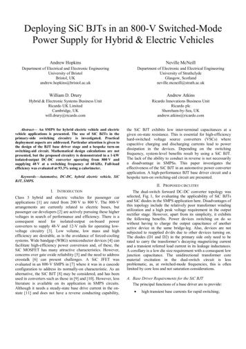
based around gapped ferrite cores and a stranded conductorwas designed for position L1 in Fig. 1.The main objective in this paper was to investigate theperformance of SiC BJTs in the SMPS’s primary-side circuitry.For simplicity, the output rectifier stage, D3 and D4 in Fig. 1,used passive SiC Schottky diodes instead of synchronousrectification (SR). These diodes were mounted on the heatsinkmarked as H2 in Fig. 8. Two small 40-mm fans were mountedonto the rear of H2, blowing air into its fins. These were SunonHA40101V4-000U-999 types. No direct forced-cooling of H1or any other component was applied, and the heatsink styleused for H1 is not optimized for naturally-cooled operation,having closely-spaced fins. It is noted that a 48-V SRarrangement for a high-efficiency SMPS output rectifier stagehas been presented in [19].T1 in Figs. 5 and 6 was arranged solely to be functional forexperimental purposes here, and this was also the case with theinsulation between N and Nr on Ls.TABLE I.R1R2CpD1-3DrCT1500 Ω (two vertically stacked 1-kΩ, 0805 resistors)11 Ω47 nF, ceramicCD214A-F150IDD03SG60CFerroxcube TN13/7.5/5 core in 3C90 material with a twoturn primary winding (N1). N2 60 turns of one strand of0.25-mm diameter copper wire.NTF3055-100T1GOne gate each from a 40106 hex inverting Schmitt trigger ICIXDN614SI driver ICTR1U1,2U3,4TABLE II.COMPONENT DATA: BASE DRIVER SIGNAL TRANSMISSIONSTAGEPrimary switchingstageRL1, 2D1-4Dz1T1H1H2T1COMPONENT DATA: LOCAL BASE DRIVER CIRCUITSL1500 Ω (two vertically stacked 1-kΩ, 0805 resistors)1N4148MMSZ5250BEpcos B64290L0632X087 core. N1 30 turns of one strandof 0.25-mm diameter copper wire. N2 N3 33 turns of onestrand of 0.2-mm diameter copper wire.NTF3055-100T1GFQT3P20TFTR1TR2TABLE III.D3,4STAGERPRELOAD1,2D1-2T1Fig. 8. Experimental hardware under test. The current transformers in each ofthe base driver circuits, Fig. 4, are located in PCB cutouts underneath heatsinkH1. D3 and D4 on heatsink H2 are each composed of four SiC Schotty diodesin parallel. (Each package shown contains two diodes in a common-cathodearrangement.) There is significant stray inductance in the transformerconnections. However, this is deemed to be beneficial here as it lumps withthe transformer’s leakage inductance to yield soft switching at TR1/2 turn-on.The local floating base driver supply voltages, VDRI, ineach case, were nominally set at 15 V. As the low-side supplyvoltage was also 15 V and the flyback transformer in Fig. 6was driven with a duty factor of 50%, the transformer wouldideally have a turns ratio of one. In practice, a slightly higherratio was used to give some allowance for losses.The three windings on the transformer used for transmittingthe base drive power and signals were physically spaced apartfrom each other. Whilst this arrangement increases leakageinductances, the capacitances between the windings areminimized. This mitigates the flow of common-mode currentsthrough these capacitances.Unlike the wound component in Figs. 5 and 6 that was usedin the base driver circuitry, the presence of common-modecapacitances between the windings on Ls is not as critical.Consequently, N and Nr on Ls were wound as a bifilar windingto maintain close coupling. This minimizes the associatedleakage inductance and maximizes the energy transferred intothe reset voltage sink, whilst also reducing the powerdissipation in Rs. The insulation between all three windings onCOMPONENT DATA: BASE DRIVER POWER TRANSMISSIONTR11 kΩ1N4148Epcos B64290L0632X087 core. N1 30 turns of onestrand of 0.25-mm diameter copper wire. N2 N3 33turns of one strand of 0.2-mm diameter copper wire.NTF3055-100T1GTABLE IV.LsCsCdRsDs, DsecCOMPONENT DATA: SWITCHING-AID CIRCUITMicrometals T80-52 core. N ten turns of 34 strands of 0.2mm diameter copper wire. Nr ten turns of one strand ofTEX-FS 0.3-mm diameter triple-insulated winding wire.4.7 nF, 2 kV, ceramic1 µF, plastic film220 Ω, 2 W, carbon filmC2D05120AIV. EXPERIMENTAL RESULTSA. WaveformsKey switching-frequency waveforms are shown in Fig. 9.Key switching transient waveforms at TR1/2 turn-on and turnoff are shown in Fig. 10. These are for operation at full powerand at rated input and output voltages.With respect to Figs. 9 and 10, it is seen that the steadystate voltage across TR2 at turn-on is pre-positioned atapproximately half the rail voltage, at 400 V. This is due to theclamping action of the output rectifier circuit during the offtime of TR1 and TR2. A reflected over-voltage of nominally48 V is seen in vTR2 at TR2 turn off. This is due to theclamping action of Nr on Ls as the current in N is commutated.With respect to Fig. 10, it is seen that, at TR1/2 turn-on, Vin
exhibits a transient fall. During this interval Ls supports aproportion of VBATT which would otherwise be applied acrossTR1 and TR2.vinB. Thermal Behavior and LossesFig. 11 shows a thermal photograph of the converter whenrunning at full load on the horizontal surface as shown inFig. 8. The circuit is in the hard thermal steady-state in Fig. 11and the ambient temperature is taken as 21 C from thebackground reading in Fig. 11. No aberrant temperature riseswere observed, and the highest temperature seen was that onthe surface of Ls, at approximately 81 C.Clampingaction herewhen Ns onLs conductsvTR20ViL10AFig. 9. Key switching-frequency waveforms. Scales: vin 200 V/div., vTR2 200 V/div., iL1 25 A/div. Time scale 2.5 µs/div.vinFig. 11. Thermal photograph of circuit in Fig. 8. The temperature of H1 isregistering as lower than its actual temperature due to the low emissivity of itssurface. The actual temperature of H1 was measured at approximately 52 Cwith a thermocouple.vTR20ViL10AThe converter was tested in a calorimeter as shown inFig. 12. The output voltage and current were measured at48.1 V and 20.9 A, giving a power of 1.005 kW. Losses weremeasured at 74.9 W. The steady-state temperature inside thecalorimetric chamber during this test was approximately 31 C.vinCalorimetricchambervTR2iL10V0AFig. 10. Key waveforms at TR1/2 turn-on (upper set of traces) and turn-off(lower set of traces). Scales: vin 200 V/div., vTR2 200 V/div., iL1 25 A/div.Time scale 50 ns/div.Fig. 12. Calorimetric set-up used for measuring efficiency.Two adjustments were made when calculating efficiency.Firstly, there was approximately 0.3 m of conductor lengthlocated between the output terminals of the converter and theentry point in the calorimeter. The nominal cross-sectional areaof this conductor was 2.5 mm2. Taking the effective length as
0.6 m and taking the resistivity of copper at 17.1 10-9 Ωm, aconductor resistance of 4.1 mΩ was calculated. At a current of21 A, this gives a loss of 1.8 W which was subtracted from theloss of 74.9 W to yield a net loss of 73.1 W. Secondly, theoutput voltage was measured at a point 1.0 m remote from theconverter output terminals. The nominal cross-sectional area ofthis conductor was also 2.5mm2. The cable loss is calculated as6.0 W, and this figure was added to the output power of1.005 kW to give 1.011 kW. An efficiency of 93.3% wastherefore calculated.base driver power transmission circuit, Fig. 6, fromentering the discontinuous mode at light loads. At avoltage of 15 V, these incur a total loss of 450 mW.The objective is to maintain continuous core fluxoperation, thus yielding a predictable open-loopvoltage gain without feedback. A cost-effective andmore efficient alternative is expected to use a primaryside output voltage sensing scheme such as that in [20].Similarly, 500-Ω pull-down resistors were used in thebase driver signal transmission circuit, Fig. 5, in thiscase to provide short signal fall times. 15 V is alsoapplied across them when TR1 and TR2 are signaledon. At a duty factor of 40%, 360 mW is dissipated.Whilst the total power consumption of 810 mW in thepre-load and pull-down resistors described here mayappear low, it represents over 8% of the loss budget ifa 99%-efficiency primary-side switching stage is beingtargeted.When making adjustments, losses in the section of the inputcabling within the calorimeter were neglected. The resistivityof copper was conservatively taken as that at 25 C. In-lineconnectors were used within the calorimeter to interface withthe outside world, and losses in these were neglected.Approximately 1.4 W of the measured power dissipation wasattributable to the two fans located on H2, and this wasincluded in the calculated loss value.As with various other power semiconductor devices, theSiC BJT exhibits a potential thermal runaway condition. In thecase of this device, its current gain falls with increasingtemperature. In particular, it can enter the active region anddevelop a high collector-emitter voltage when it is on. Thisincreases the conduction losses, in turn raising its temperatureand further reducing its gain. It is therefore necessary to ensurethat the combination of heatsink thermal resistance and basecurrent is appropriate to avoid thermal runaway for the worstcase ambient temperature and operating conditions that will beencountered. The base current in the circuitry here is primarilydetermined by the turns-ratio of the CT used in the base drivercircuits, and this ratio has to be set appropriately to avoidthermal runaway. The input switching-aid circuit using the inductance Lsin Fig. 7 removes losses from TR1 and TR2. However,the leakage inductance of T1 in Figs. 1 and 8 alsoprovides a desirable turn-on snubbering effect. Thenecessity or otherwise, of incorporating an inputswitching-aid circuit can be investigated, along withoptimization of T1’s leakage inductance. The BJTs used have a quoted on-state resistance of100 mΩ at 25 C. A corollary of a low on-stateresistance is high inter-terminal capacitances withconsequent losses associated with their charging anddischarging during switching transients. Conversely,whilst a higher on-state resistance introduces higherconduction losses, capacitive losses are expected to belower. Notwithstanding cost issues, further work isrequired to establish the optimum on-state resistancefor further improving efficiency in this application.Similarly, the die size of the diodes in the primarystage may be addressed. The heatsinks (H1 and H2) were essentially nonoptimized placeholders and small fans were used tocool the output rectifier stage on H2. Further work willalso include developing hardware without forcedcooling. This will include optimized heat dissipationand introducing SR in the output rectifier stage. In thedual-switch forward converter, this stage has to supporta higher voltage than is the case with topologies suchas the full-bridge converter in [7]. It is consequentlynecessary to use higher-voltage rated MOSFETs in itwith different capacitance and reverse-recoverycharacteristics.V. DISCUSSIONA qualitative description of the circuitry presented has beengiven. Several aspects of the circuit’s performance may beinvestigated further and some of these are discussed here: The base driver performance can be investigated withthe objective of attaining faster switching speeds. Thevalues of components, in particular Cp and R2 inFig. 4, may be optimized. It is noted that the signalsfrom the differential output stages in Fig. 4 shouldideally be in exact antiphase. However, a propagationdelay is expected due to U2, and this consequentlyintroduces a delay into the output signal produced byU3 with respect to that of U4. The effect on switchingspeeds may be assessed. Alternatives are to use a noninverting and an inverting driver IC with matchedpropagation delays in positions U3 and U4respectively, or replace these with a single driver ICwith complementary outputs (without dead-times). Asdescribed in Section IV, it is also necessary todetermine the minimum safe base-drive current settingto avoid thermal runaway under worst-case conditions,and configure the base driver circuits appropriately.1-kΩ pre-load resistances were included in the localfloating base driver supplies to prevent the flybackVI. CONCLUSIONAn isolated-output power converter for hybrid electricvehicle applications using SiC BJTs has been presented. Theconverter operates from an input voltage of 800 V and supplies48 V at an output power of 1 kW. The switching frequency was60 kHz and the full-load efficiency was measured at 93.3%.The focus of this paper has been on the primary-side switchingcircuitry. Practical deployment issues have been addressed in a
qualitative manner, including the use of ancillary magneticcircuitry. It is concluded that the SiC BJT is effective in thisapplication and yields system-level benefits.
current. Further details of its operation in this mode are given in [14]. Whilst in [14] a negative base-emitter off-stage voltage is provided by a circuit using a third supply rail, the CT’s operation is essentially the same in the circuit here. TR5 acts as a switch to disconnect CT1 from the emi