Transcription
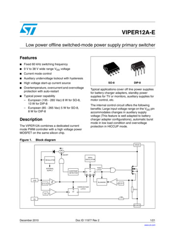
VIPER12A-ELow power offline switched-mode power supply primary switcherFeatures Fixed 60 kHz switching frequency 9 V to 38 V wide range VDD voltage Current mode control Auxiliary undervoltage lockout with hysteresis High voltage start-up current source Overtemperature, overcurrent and overvoltageprotection with auto-restart Typical power capability– European (195 - 265 Vac) 8 W for SO-8,13 W for DIP-8– European (85 - 265 Vac) 5 W for SO-8,8 W for DIP-8SO-8Typical applications cover off line power suppliesfor battery charger adapters, standby powersupplies for TV or monitors, auxiliary supplies formotor control, etc.The internal control circuit offers the followingbenefits: Large input voltage range on the VDD pinaccommodates changes in auxiliary supplyvoltage (This feature is well adapted to batterycharger adapter configurations), automatic burstmode in low load condition and overvoltageprotection in HICCUP mode.DescriptionThe VIPER12A combines a dedicated currentmode PWM controller with a high voltage powerMOSFET on the same silicon chip.Figure 1.DIP-8Block SUPPLYOVERTEMP.DETECTORR1SFFPWMLATCHQR2 R3 R4VDD8/14.5V BLANKING 42VSRFF0.23 VOVERVOLTAGELATCH230 ΩQ1 kΩFBSOURCEDecember 2010Doc ID 11977 Rev 21/21www.st.com21
ContentsVIPER12A-EContents1Electrical data . . . . . . . . . . . . . . . . . . . . . . . . . . . . . . . . . . . . . . . . . . . . . . 31.1Maximum rating . . . . . . . . . . . . . . . . . . . . . . . . . . . . . . . . . . . . . . . . . . . . . 31.2Thermal data . . . . . . . . . . . . . . . . . . . . . . . . . . . . . . . . . . . . . . . . . . . . . . . 32Electrical characteristics . . . . . . . . . . . . . . . . . . . . . . . . . . . . . . . . . . . . . 43Pin connections and function . . . . . . . . . . . . . . . . . . . . . . . . . . . . . . . . . 64Rectangular U-I output characteristics . . . . . . . . . . . . . . . . . . . . . . . . . . 75Wide range of VDD voltage . . . . . . . . . . . . . . . . . . . . . . . . . . . . . . . . . . . 86Feedback pin principle of operation . . . . . . . . . . . . . . . . . . . . . . . . . . . . 97Startup sequence . . . . . . . . . . . . . . . . . . . . . . . . . . . . . . . . . . . . . . . . . . 118Overvoltage threshold . . . . . . . . . . . . . . . . . . . . . . . . . . . . . . . . . . . . . . 129Operation pictures . . . . . . . . . . . . . . . . . . . . . . . . . . . . . . . . . . . . . . . . . 1310Package mechanical data . . . . . . . . . . . . . . . . . . . . . . . . . . . . . . . . . . . . 1611Order codes . . . . . . . . . . . . . . . . . . . . . . . . . . . . . . . . . . . . . . . . . . . . . . . 1912Revision history . . . . . . . . . . . . . . . . . . . . . . . . . . . . . . . . . . . . . . . . . . . 202/21Doc ID 11977 Rev 2
VIPER12A-EElectrical data1Electrical data1.1Maximum ratingStressing the device above the rating listed in the “absolute maximum ratings” table maycause permanent damage to the device. These are stress ratings only and operation of thedevice at these or any other conditions above those indicated in the Operating sections ofthis specification is not implied. Exposure to absolute maximum rating conditions forextended periods may affect device reliability.Table 1.Absolute maximum ratingSymbolVDS(sw)VDS(st)IDParameterUnit-0.3 . 730V-0.3 . 400VInternally limitedA0 . 50V3mA2001.5VkVInternally limited CSwitching drain source voltage (TJ 25 . 125 C) (1)Start-up drain source voltage (TJ 25 . 125 C)(2)Continuous drain currentVDDSupply voltageIFBFeedback currentVESDValueElectrostatic discharge:Machine model (R 0 Ω; C 200 pF)Charged device modelTJJunction operating temperatureTCCase operating temperature-40 to 150 CTstgStorage temperature-55 to 150 C1. This parameter applies when the start-up current source is OFF. This is the case when the VDD voltage hasreached VDDon and remains above VDDoff.2. This parameter applies when the start up current source is ON. This is the case when the VDD voltage hasnot yet reached VDDon or has fallen below VDDoff.1.2Thermal dataTable 2.SymbolThermal dataParameterSO-8DIP-8UnitRthJCThermal resistance junction-caseMax2515 C/WRthJAThermal resistance ambient-case (1)Max5545 C/W1. When mounted on a standard single-sided FR4 board with 200 mm2 of Cu (at least 35 µm thick) connectedto all DRAIN pins.Doc ID 11977 Rev 23/21
Electrical characteristics2VIPER12A-EElectrical characteristicsTJ 25 C, VDD 18 V, unless otherwise specifiedTable 3.Power sectionSymbolParameterBVDSSDrain-source voltageID 1 mA; VFB 2 VOFF State draincurrentVDS 500 V; VFB 2 V;TJ 125 CStatic drain-sourceON state resistanceID 0.2 A ID 0.2 A;IDSSrDS(on)Test conditionsMinTypMax730UnitV0.127ID 0.2 A ID 0.2 A; TJ 100 C30mAΩ54tfFall timeID 0.1 A; VIN 300 V (1)(See Figure 9 on page 13)100nstrRise timeID 0.2 A; VIN 300 V (1)(See Figure 9 on page 13)50nsDrain capacitanceVDS 25 V40pFCOSS1. On clamped inductive loadTable 4.SymbolSupply sectionParameterTest conditionsMinTypMaxIDDchStart-up chargingcurrent100 V VDS 400 V;VDD 0 V .VDDon(See Figure 10 on page 13)IDDoffStart-up chargingcurrent in thermalshutdownVDD 5 V; VDS 100 VTJ TSD - THYSTIDD0Operating supplycurrent not switchingIFB 2 mAIDD1Operating supplycurrent switchingIFB 0.5 mA; ID 50 mA (1)4.5mADRSTRestart duty-cycle(See Figure 11 on page 13)16%VDDoffVDD undervoltageshutdown threshold(See Figure 10,Figure 11 on page 13)789VVDDonVDD start-upthreshold(See Figure 10,Figure 11 on page 13))1314.516VVDDhystVDD thresholdhysteresis(See Figure 10 on page 13)5.86.57.2VVDDovpVDD overvoltagethreshold384246V-1mA0mA351. These test conditions obtained with a resistive load are leading to the maximum conduction time of thedevice.4/21UnitDoc ID 11977 Rev 2mA
VIPER12A-EElectrical characteristicsTable 5.SymbolFOSCTable 6.SymbolOscillation sectionParameterOscillator frequencytotal variationTest conditionsVDD VDDoff . 35 V;TJ 0 . 100 CMinTypMaxUnit546066kHzMinTypMaxUnit0.48APWM comparator sectionParameterTest conditionsGIDIFB to ID current gain(See Figure 12 on page 14)IDlimPeak currentlimitationVFB 0 V(See Figure 12 on page 14)IFBsdIFB shutdown current(See Figure 12 on page 14)0.9mARFBFB pin inputimpedanceID 0 mA(See Figure 12 on page 14)1.2kΩtdCurrent sense delayto turn-OFFID 0.2 A200nstbBlanking time500nsMinimum Turn-ONtime700nstONminTable 7.Symbol0.320.4Overtemperature sectionParameterTest conditionsTSDThermal shutdowntemperature(See Figure 13 on page 14)THYSTThermal shutdownhysteresis(See Figure 13 on page 14)Table 8.320MinTypMaxUnit140170 C40 CTypical power capabilityMains typeSO-8DIP-8European (195 - 265 Vac)8W13WUS / Wide range (85 - 265 Vac)5W8WDoc ID 11977 Rev 25/21
Pin connections and function3VIPER12A-EPin connections and functionFigure 2.Pin SO-8Figure 3.DIP-8Current and voltage conventionsI DDIDVDDI FBFBVDDVFBTable 9.CONTROLVDSOURCEVIPer12APin functionPin NamePin FunctionVDDPower supply of the control circuits. Also provides a charging current during start upthanks to a high voltage current source connected to the drain. For this purpose, anhysteresis comparator monitors the VDD voltage and provides two thresholds:- VDDon: Voltage value (typically 14.5 V) at which the device starts switching and turnsoff the start up current source.- VDDoff: Voltage value (typically 8 V) at which the device stops switching and turns onthe start up current source.SOURCE6/21DRAINPower MOSFET source and circuit ground reference.DRAINPower MOSFET drain. Also used by the internal high voltage current source duringstart up phase for charging the external VDD capacitor.FBFeedback input. The useful voltage range extends from 0 V to 1 V, and defines thepeak drain MOSFET current. The current limitation, which corresponds to themaximum drain current, is obtained for a FB pin shorted to the SOURCE pin.Doc ID 11977 Rev 2
VIPER12A-E4Rectangular U-I output characteristicsRectangular U-I output characteristicsFigure 4.Rectangular U-I output characteristics for battery chargerA complete regulation scheme can achieve combined and accurate output characteristics.Figure 4. presents a secondary feedback through an optocoupler driven by a TSM101. Thisdevice offers two operational amplifiers and a voltage reference, thus allowing the regulationof both output voltage and current. An integrated OR function performs the combination ofthe two resulting error signals, leading to a dual voltage and current limitation, known as arectangular output characteristic. This type of power supply is especially useful for batterychargers where the output is mainly used in current mode, in order to deliver a definedcharging rate. The accurate voltage regulation is also convenient for Li-ion batteries whichrequire both modes of operation.Doc ID 11977 Rev 27/21
Wide range of VDD voltage5VIPER12A-EWide range of VDD voltageThe VDD pin voltage range extends from 9 V to 38 V. This feature offers a great flexibility indesign to achieve various behaviors. In Figure 4 on page 7 a forward configuration has beenchosen to supply the device with two benefits:8/21 As soon as the device starts switching, it immediately receives some energy from theauxiliary winding. C5 can be therefore reduced and a small ceramic chip (100 nF) issufficient to insure the filtering function. The total start up time from the switch on ofinput voltage to output voltage presence is dramatically decreased. The output current characteristic can be maintained even with very low or zero outputvoltage. Since the TSM101 is also supplied in forward mode, it keeps the currentregulation up whatever the output voltage is.The VDD pin voltage may vary as much asthe input voltage, that is to say with a ratio of about 4 for a wide range application.Doc ID 11977 Rev 2
VIPER12A-E6Feedback pin principle of operationFeedback pin principle of operationA feedback pin controls the operation of the device. Unlike conventional PWM controlcircuits which use a voltage input (the inverted input of an operational amplifier), the FB pinis sensitive to current. Figure 5. presents the internal current mode structure.Figure 5.Internal current control structureThe power MOSFET delivers a sense current Is which is proportional to the main current Id.R2 receives this current and the current coming from the FB pin. The voltage across R2 isthen compared to a fixed reference voltage of about 0.23 V. The MOSFET is switched offwhen the following equation is reached:R 2 ( I S I FB ) 0.23VBy extracting IS:0.23VI S ---------------- – I FBR2Using the current sense ratio of the MOSFET GID:I D G ID I S G ID 0.23V---------------- – I FB R 2Doc ID 11977 Rev 29/21
Feedback pin principle of operationVIPER12A-EThe current limitation is obtained with the FB pin shorted to ground (VFB 0 V). This leadsto a negative current sourced by this pin, and expressed by:I FB – 0.23V---------------R1By reporting this expression in the previous one, it is possible to obtain the drain currentlimitation IDlim:11I Dlim G ID 0.23V ------- ------- R2 R1In a real application, the FB pin is driven with an optocoupler as shown on Figure 5 whichacts as a pull up. So, it is not possible to really short this pin to ground and the above draincurrent value is not achievable. Nevertheless, the capacitor C is averaging the voltage onthe FB pin, and when the optocoupler is off (start up or short circuit), it can be assumed thatthe corresponding voltage is very close to 0 V.For low drain currents, the formula (1) is valid as long as IFB satisfies IFB IFBsd, whereIFBsd is an internal threshold of the VIPER12A. If IFB exceeds this threshold the device willstop switching. This is represented on Figure 12 on page 14, and IFBsd value is specified inthe PWM COMPARATOR SECTION. Actually, as soon as the drain current is about 12 % ofIdlim, that is to say 50 mA, the device will enter a burst mode operation by missing switchingcycles. This is especially important when the converter is lightly loaded.Figure 6.IFB transfer functionIt is then possible to build the total DC transfer function between ID and IFB as shown onFigure 6 on page 10. This figure also takes into account the internal blanking time and itsassociated minimum turn on time. This imposes a minimum drain current under which thedevice is no more able to control it in a linear way. This drain current depends on the primaryinductance value of the transformer and the input voltage. Two cases may occur, dependingon the value of this current versus the fixed 50 mA value, as described above.10/21Doc ID 11977 Rev 2
VIPER12A-E7Startup sequenceStartup sequenceFigure 7.Startup sequenceThis device includes a high voltage start up current source connected on the drain of thedevice. As soon as a voltage is applied on the input of the converter, this start up currentsource is activated as long as VDD is lower than VDDon. When reaching VDDon, the start upcurrent source is switched off and the device begins to operate by turning on and off its mainpower MOSFET. As the FB pin does not receive any current from the optocoupler, thedevice operates at full current capacity and the output voltage rises until reaching theregulation point where the secondary loop begins to send a current in the optocoupler. Atthis point, the converter enters a regulated operation where the FB pin receives the amountof current needed to deliver the right power on secondary side.This sequence is shown in Figure 7. Note that during the real starting phase tss, the deviceconsumes some energy from the VDD capacitor, waiting for the auxiliary winding to provide acontinuous supply. If the value of this capacitor is too low, the start up phase is terminatedbefore receiving any energy from the auxiliary winding and the converter never starts up.This is illustrated also in the same figure in dashed lines.Doc ID 11977 Rev 211/21
Overvoltage threshold8VIPER12A-EOvervoltage thresholdAn overvoltage detector on the VDD pin allows the VIPER12A to reset itself when VDDexceeds VDDovp. This is illustrated in Figure 8., which shows the whole sequence of anovervoltage event. Note that this event is only latched for the time needed by VDD to reachVDDoff, and then the device resumes normal operation automatically.Figure 8.Overvoltage sequenceVDDVDDovpVDDonVDDofftVDSt12/21Doc ID 11977 Rev 2
VIPER12A-E9Operation picturesOperation picturesFigure 9.Rise and fall timeFigure 10. Start-up VDD currentIDDIDD0VDDhystVDDoffIDDchVDDVDDonVDS 100 VFsw 0 kHzFigure 11. Restart duty-cycleDoc ID 11977 Rev 213/21
Operation picturesVIPER12A-EFigure 12. Peak drain current vs feedback currentFigure 13. Thermal shutdown14/21Doc ID 11977 Rev 2
VIPER12A-EOperation picturesFigure 14. Switching frequency vs temperatureFigure 15. Current limitation vs temperatureDoc ID 11977 Rev 215/21
Package mechanical data10VIPER12A-EPackage mechanical dataIn order to meet environmental requirements, ST offers these devices in different grades ofECOPACK packages, depending on their level of environmental compliance. ECOPACK specifications, grade definitions and product status are available at: www.st.com. ECOPACKis an ST trademark.16/21Doc ID 11977 Rev 2
VIPER12A-EPackage mechanical dataTable 10.DIP8 mechanical dataDatabook ackage Weight3.303.81Gr. 470Figure 16. Package dimensionsDoc ID 11977 Rev 217/21
Package mechanical dataTable 11.VIPER12A-ESO8 mechanical dataDatabook 50L0.401.27k8 (max.)ddd0.1Figure 17. Package dimensions18/21MinDoc ID 11977 Rev 2
VIPER12A-E11Order codesOrder codesTable 12.Order codesOrder codesPackagePackagingVIPER12ASTR-ESO-8Tape and reelVIPER12AS-ESO-8TubeVIPER12ADIP-EDIP-8TubeDoc ID 11977 Rev 219/21
Revision history12VIPER12A-ERevision historyTable 13.20/21Document revision historyDateRevisionChanges09-Jan-20061Initial release.13-Dec-20102Updated Table 3 on page 4, Table 4 on page 4 and Figure 10on page 13.Doc ID 11977 Rev 2
VIPER12A-EPlease Read Carefully:Information in this document is provided solely in connection with ST products. STMicroelectronics NV and its subsidiaries (“ST”) reserve theright to make changes, corrections, modifications or improvements, to this document, and the products and services described herein at anytime, without notice.All ST products are sold pursuant to ST’s terms and conditions of sale.Purchasers are solely responsible for the choice, selection and use of the ST products and services described herein, and ST assumes noliability whatsoever relating to the choice, selection or use of the ST products and services described herein.No license, express or implied, by estoppel or otherwise, to any intellectual property rights is granted under this document. If any part of thisdocument refers to any third party products or services it shall not be deemed a license grant by ST for the use of such third party productsor services, or any intellectual property contained therein or considered as a warranty covering the use in any manner whatsoever of suchthird party products or services or any intellectual property contained therein.UNLESS OTHERWISE SET FORTH IN ST’S TERMS AND CONDITIONS OF SALE ST DISCLAIMS ANY EXPRESS OR IMPLIEDWARRANTY WITH RESPECT TO THE USE AND/OR SALE OF ST PRODUCTS INCLUDING WITHOUT LIMITATION IMPLIEDWARRANTIES OF MERCHANTABILITY, FITNESS FOR A PARTICULAR PURPOSE (AND THEIR EQUIVALENTS UNDER THE LAWSOF ANY JURISDICTION), OR INFRINGEMENT OF ANY PATENT, COPYRIGHT OR OTHER INTELLECTUAL PROPERTY RIGHT.UNLESS EXPRESSLY APPROVED IN WRITING BY AN AUTHORIZED ST REPRESENTATIVE, ST PRODUCTS ARE NOTRECOMMENDED, AUTHORIZED OR WARRANTED FOR USE IN MILITARY, AIR CRAFT, SPACE, LIFE SAVING, OR LIFE SUSTAININGAPPLICATIONS, NOR IN PRODUCTS OR SYSTEMS WHERE FAILURE OR MALFUNCTION MAY RESULT IN PERSONAL INJURY,DEATH, OR SEVERE PROPERTY OR ENVIRONMENTAL DAMAGE. ST PRODUCTS WHICH ARE NOT SPECIFIED AS "AUTOMOTIVEGRADE" MAY ONLY BE USED IN AUTOMOTIVE APPLICATIONS AT USER’S OWN RISK.Resale of ST products with provisions different from the statements and/or technical features set forth in this document shall immediately voidany warranty granted by ST for the ST product or service described herein and shall not create or extend in any manner whatsoever, anyliability of ST.ST and the ST logo are trademarks or registered trademarks of ST in various countries.Information in this document supersedes and replaces all information previously supplied.The ST logo is a registered trademark of STMicroelectronics. All other names are the property of their respective owners. 2010 STMicroelectronics - All rights reservedSTMicroelectronics group of companiesAustralia - Belgium - Brazil - Canada - China - Czech Republic - Finland - France - Germany - Hong Kong - India - Israel - Italy - Japan Malaysia - Malta - Morocco - Philippines - Singapore - Spain - Sweden - Switzerland - United Kingdom - United States of Americawww.st.comDoc ID 11977 Rev 221/21
December 2010 Doc ID 11977 Rev 2 1/21 21 VIPER12A-E Low power offline switched-mode power supply primary switcher Features Fixed 60 kHz switching frequency 9 V to 38 V wide range VDD voltage Current mode control Auxiliary undervoltage lockout with hysteresis High voltage start-up curren