Transcription
1800IEEE SENSORS JOURNAL, VOL. 11, NO. 9, SEPTEMBER 2011Embedded Runtime Reconfigurable Nodes forWireless Sensor Networks ApplicationsYana Esteves Krasteva, Jorge Portilla, Eduardo de la Torre, and Teresa RiesgoAbstract—The use of reconfigurable hardware (HW) can improve the processing performance of many systems, includingWireless Sensor Networks (WSNs). Moreover, reconfigurabledevices permit remote and runtime HW reconfiguration, whichimplies benefits in WSNs deployment and maintainability and,finally, cost reduction.In this paper, WSN node runtime reconfigurability is tackledfrom several aspects. First, the sensor node includes a commercialreconfigurable device, a Field Programmable Gate Array (FPGA),that permits to take advantage of the tools and support providedby the industry, while exploiting the inherent hardware parallelism. Second, two software (SW) and hardware reconfigurationscenarios are defined along with a support middleware. Third,in order to provide runtime reconfigurability to the WSN node,a complete runtime reconfigurable system has been defined anddesigned for the FPGA included in the node. Fourth, the HWreconfiguration cost has been evaluated, as well as the cost oftransmitting new HW configurations and SW programs throughthe network, based on a set of defined parameters. Finally, thefeasibility of the runtime reconfigurable system has been demonstrated with a use case.Index Terms—Embedded systems, field programmable gate arrays (FPGAs), reconfigurable architectures, wireless sensor networks (WSNs).I. INTRODUCTIONWIRELESS SENSOR NETWORKS (WSNs) representone of the most challenging areas in today’s electronicindustry [1], [2]. These networks are expected to be autonomous, low-power demanding, context aware, and flexible.A final application may have hundreds or thousands of sensornodes spread out in an environment, making the deploymentand the support of WSNs a complex task. Although the integration technologies are clearly tending to smart sensor, thereis still an increasing variety of sensors. The interfaces and dataprocessing required for sensors control are very different notonly from one sensor to another, but also from one applicationto another. In such context, the use of identical nodes or areduced set of nodes that are further adapted and/or customizedwould simplify the deployment process and reduce the productcost.Manuscript received September 06, 2010; revised December 03, 2010; accepted December 31, 2010. Date of publication January 10, 2011; date of current version July 27, 2011. The associate editor coordinating the review of thispaper and approving it for publication was Prof. Ralph Etienne-Cummings.The authors are with the Centro de Electrónica Industrial, UniversidadPolitécnica de Madrid, Jose Gutierrez Abascal 2, 28006, Madrid, Spain (e-mail:yana.ekrasteva@upm.es; jorge.portilla@upm.es; or versions of one or more of the figures in this paper are available onlineat http://ieeexplore.ieee.org.Digital Object Identifier 10.1109/JSEN.2011.2104948Classic design approaches for WSNs node rely on the useof a microcontroller ( C) [3], [4]. However, processing andfunctionality needs are continuously increasing due to new application requirements and this includes WSNs applications.This, added to the constantly increasing pressure for reducingtime-to-market, has led to new design alternatives, such as reconfigurable hardware (HW).Reconfigurable systems have been studied in the last yearsas an alternative for both: Application-Specific Integrated Circuits (ASICs) and General Purpose Processors (GPPs). GPPs,for instance, suffer an imbalance between IO (device Input-Outputs) and processing. Differently, FPGAs provide not only alarge amount of IOs, but also high processing due to the offered inherited of parallelism and pipelining. Furthermore, reconfigurable systems provide high flexibility as they can be updated after system deployment and also permit time to marketreduction, since the proper prototype can be the final device. Asa result, reconfigurable devices are constantly gaining marketshare and extending their industry application domains and research interest [5], [6]. For instance, the work presented in [7]focuses on the application of FPGAs in industry control systems. Even more, now, it is possible to implement neural networks and fuzzy control solutions on FPGAs [8] and also, reconfigurable computing has been widely explored in acceleratingapplications, like calculations related to molecular dynamics in[9].This paper is focused on the use of reconfigurable systems inWSNs. Several research groups have already exploited the benefits of HW parallelism by designing ad-hoc reconfigurable devices prepared to be adapted to a set of prerecorded applications,like in [10] and [11]. The flexibility achieved with this approachis higher compared to ASIC-based solutions, but not as high aswith small grain reconfigurable devices, like FPGAs. In addition to this, custom solutions are more restricted as they requirespecific Computer Aided Design (CAD) tools. Differently, thispaper exploits industry available reconfigurable devices lookingfor high adaptability and flexibility through the use of the partial runtime reconfiguration technique, while taking advantageof the vendor provided CAD tools. In particular, this paper aimsto explore and evaluate the use of partial runtime reconfigurationin WSNs, topic that has not been explored in the state-of-the-art.Runtime reconfiguration is an advanced topic within thereconfigurable computing area, where changes into the FPGAconfiguration are done at runtime, while the device I/Os andremaining logic is kept active. This powerful feature (onlyincluded in Xilinx and Atmel FPGAs) permits not only toperform HW updates at runtime and at anytime, but also tosave memory space and programming time compared to fullFPGA reconfiguration. Partial reconfiguration has already been1530-437X/ 26.00 2011 IEEE
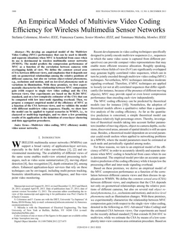
KRASTEVA et al.: EMBEDDED RUNTIME RECONFIGURABLE NODES FOR WIRELESS SENSOR NETWORKS APPLICATIONSexploited in the automotive industry [12] and in shape-adaptivevideo applications [13], where different reconfiguration strategies are studied.Runtime reconfiguration will be tested in a HW platform forWSNs developed at CEI, called Cookies and first presented in[14]. This platform is overviewed in the paper, along with anoutline of the WSNs state-of-the-art, in order to highlight itsdistinguishing characteristics.This paper describes the entire reconfigurable system design that includes: the definition of the node reconfigurabilityscenarios, the support SW definition and implementation and,a detailed description of the partial runtime reconfigurablesystem definition and design process. In order to test the designed system, a work flow, also described in this paper, hasbeen used to generate node HW configurations. Furthermore,a set of general parameters have been defined to evaluate thesystem reconfiguration cost and applied to the target node.Finally, a partial runtime reconfiguration use case has beencreated to validate the feasibility of remote runtime reconfiguration in WSNs.The rest of this paper is organized as follows. Section II includes the review of the available industrial and academic WSNalong with the brief description of the Cookie modular node architecture. The identified node reconfiguration scenarios, alongwith a general view of a reconfiguration control middleware,are included in Section III. Section IV presents the design ofthe proposed partial runtime reconfiguration system for WSNand the complete reconfiguration workflow. A system evaluation based on general reconfiguration cost parameters and theresults can be found in Section V. A discussion of some reconfigurable system aspects related to WSN nodes can be found inSection VI. Finally, conclusions are included in Section VII.II. COOKIE SENSOR NODEIn this section, a general state-of-the-art in HW platformsfor WSNs nodes is presented. Both industrial and academicapproaches are presented. The Cookie node is described inSection II-B.A. WSNS Hardware Platforms State-of-the-ArtSeveral HW platforms with different approaches have beendeveloped by different research groups during the last years.Most of them present a SW point-of-view in which the core ofthe processing stage is a microcontroller. Researchers from UCBerkeley developed the TelosB sensor node, one of the widelyused platforms for WSN research and development [3]. Thisplatform is based on an ultra-low-power microcontroller and alow data rate low-power IEEE 802.15.4 [15] compliant radiochip. Sensors can be added to the platform through an expansionconnector. Hitachi has developed a sensor node with a modularapproach [4], based on a microcontroller resized for dimensionreduction, proprietary battery technology and IEEE 802.15.4compliant radio chip.These are two examples of SW-based platforms for WSNs.Although they are very good solutions, they are resource limited, so in high data processing applications, problems relatedto overhead can occur.1801Traditionally, reconfigurable devices like Complex Programmable Logic Devices (CPLDs) or FPGAs are not includedin designs for sensor nodes, mainly due to their high powerconsumption. On the other hand, solutions in which suchdevices are integrated can target a wider set of computationallyintensive applications, as well as adding flexibility to the sensornode. For example, in the platform used in the present work, aSpartan 3 FPGA from Xilinx and an ADuC841 microcontrollerfrom Analog Devices are used to carry out the processing tasks.There is a processing layer version, to be available in the nearfuture, composed of a MSP430 microcontroller from TexasInstruments and an Actel Igloo FPGA. This low-power versionwill consume 10 A in sleep mode, which is a real competitivepower consumption value compared with the state-of-the-artplatforms. As a reference, the Cookie node version used inthis paper consumes 30 mA, while the widely used CrossbowTelosB platform that does not include HW reconfigurabilityconsumes 5.1 A (in standby mode).However, some solutions for WSN nodes include reconfigurable HW elements. A modular reconfigurable platform hasbeen developed by Microsoft Research Labs [16]. In this platform, several layers can be added to the final platform, withseveral microprocessors depending on the application requirements, and the reconfigurable HW (CPLD in this case) is used toachieve communication abstraction through the entire modularplatform. Therefore, the processors within the platform communicate directly with the CPLD, which makes possible differentfinal implementations. Tyndall National Institute has developedanother modular platform [17], which allows the inclusion of anFPGA layer to carry out Digital Signal Processing (DSP) tasks.They make a division between processing, sensing, communication, and power supply, which is the way in which the sensornodes functionality is divided.The groups described in the previous paragraph use commercial reconfigurable devices in their designs. On the other hand,other groups work in developing new integrated circuits, whichincorporate reconfigurable HW as part of the entire circuit. In[10], a specific integrated circuit with a microcontroller unit anda reconfigurable part is presented. Their goal is to provide thenode with flexibility in order to adapt it to environment changes.In [11], an approach in which the system adapts itself to executethe tasks more efficiently, in terms of power, is presented.B. Cookie Sensor NodeThe distinguishing characteristic in Cookie is that it has beendesigned in order to provide flexibility and adaptability, by applying modularity at the physical HW level through a layeredprinted circuit board (PCB) structure (see Fig. 1) and providingit with reconfigurable HW (FPGA).Modularity allows dividing and encapsulating the functionality included in the node. Therefore, future redesigns mayinvolve only part of the platform, which is desirable considering time-to-market and evolving technologies and standards.Moreover, due to the node flexibility, it is possible to carry outa design space exploration for the HW node, by interchangingdifferent implementations for each layer, depending on theapplication.
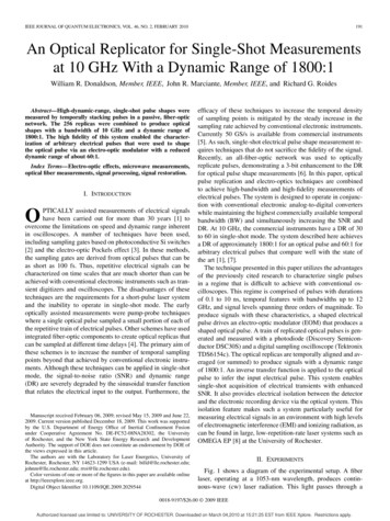
1802IEEE SENSORS JOURNAL, VOL. 11, NO. 9, SEPTEMBER 2011Fig. 2. Sensor node system architecture. Analog sensors are connected to theuC ADCs, while digital sensors are connected to the FPGA.Fig. 1. On the top part, the Cookie processing layer (uC on the left and theFPGA on the right) and on the bottom, a complete Cookie node.The Cookie is composed of four main layers (more layerscan be added in future versions): processing, communications,power supply, and sensors. Every layer carries out a specifictask. In the following paragraphs, these layers are detailed.1) Processing: This is the heart of the node. It includes an8051 microcontroller core enhanced with several peripherals from Analog Devices (ADuC841) and a XilinxXC3S200 Spartan 3 FPGA. The microcontroller and theFPGA share three 8-bit ports for communication. Part ofone port of the microcontroller is connected to the JoinTest Action Group (JTAG, IEEE 1149.1 [18] standard)programming port of the FPGA.2) Communications: The last version of this layer includesa ZigBee module (ETRX2 from Telegesis). This moduleis managed by the microcontroller through the UniversalAsynchronous Receiver Transmitter (UART) port. Anotherlayer version with Bluetooth is also available.3) Power supply: This layer generates all voltages neededwithin the Cookie. Two versions have been developed. Theone used in the work presented in this paper includes a Universal Serial Bus (USB) connection, which allows powersupply from a PC, as well as serial programming for theC.4) Sensors: This layer includes those elements which are intended to take measurements from the environment. Threedifferent layers have been developed for the Cookie. Theselayers include sensors of acceleration, temperature, humidity, light, infrared, and deformation (strain gauge).Additionally, other layers can be added to the modular platform like, for instance, a memory layer suitable for expandingthe microcontroller program memory and/or for holding a HWconfiguration library.One of the features of the sensor layer is that it can includesensors with both digital and analog interfaces (they will becalled digital sensors and analog sensors respectively from nowon). In Fig. 2, the architecture of the system is shown. Signalsfrom analog sensors are connected to the ADC of the microcontroller. On the other hand, signals from digital sensors areconnected to the FPGA. In principle, the FPGA carries out allprocessing related to digital sensors in order to release the Cthat is in charge of managing the node communications and processing data from analog sensors. Nevertheless, if an externalADC is included in a sensor layer version, analog sensors couldbe directly connected to the FPGA.Nowadays, there are a myriad of sensors in the market withseveral different interfaces. Many of them are digital sensors,with different protocols such as SPI, I2C, 1-Wire, etc. Whenthis kind of signals have to be processed using a microcontroller,problems related to timing and processor overhead can appear.In fact, some manufacturers offer Hardware Description Language (HDL) code to implement the sensor interfaces in a coprocessor, for instance, Dallas Semiconductor with its 1-Wireinterface [19].In this context, a proprietary library of generic HW interfaces [20] has been developed in order to process sensor signalswith very different digital interfaces. Currently, the interfacesincluded in the library are as follows. I2C and I2C modified (interface for Sensirion Companysensors). PWM. Period/Frequency. 1-Wire.The library is divided in modules which represent sensorinterfaces (actuator interfaces can be added as well). Everymodule has been designed following a philosophy inspired inthe IEEE 1451 family of standards, but they can also be usedwithout being compatible to them. Each sensor or actuator(transducer) is “seen” as a channel (or set of channels) by thetransducer controller. Two channel types are recognized: sensorchannel and actuator channel. Some sensors, like the SHT11from Sensirion, supply two or more measures (in this case,humidity and temperature). Therefore, for the same sensor, twodifferent channels are needed.The microcontroller sends triggers to the FPGA, specifyingthe sensor from which the measure has to be taken, and theFPGA activates the appropriate sensor interface. Then, theFPGA sends the result to the microcontroller. The FPGA actsas a reconfigurable coprocessor for the microcontroller bytaking the signals from the digital sensors, and processingthe information for the microcontroller. In other cases, thiscoprocessing cannot be made by the microcontroller, such asthe case of relatively complex filtering stages, which could notbe covered due to data bandwidth restrictions.
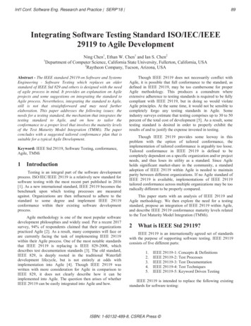
KRASTEVA et al.: EMBEDDED RUNTIME RECONFIGURABLE NODES FOR WIRELESS SENSOR NETWORKS APPLICATIONS1803These interfaces along with HW coprocessing in the FPGAwill be used to show the runtime reconfiguration capabilities ofthe platform, using partial reconfiguration techniques.III. NODE RECONFIGURATION SCENARIOS AND CONTROL SWIn this paper, node reconfigurability is associated not onlywith loading new SW programs in the microcontroller (SW reprogramming), but also new HW configurations in the reconfigurable fabric (HW reconfiguration). Related to this, two generalreconfiguration scenarios have been differentiated and appliedto the Cookie node. The first one covers reconfiguration at network level that ismostly required during deployment, where the final function of each network node is defined (this includes the usedsensors and data processing) or, when the network function is changed (like in an emergency situation). Generally this scenario may cover both, SW reprogramming andHW reconfiguration. In the context of the Cookie platform,HW reconfiguration is mandatory when modifications affect digital sensors (marked with “D” in Fig. 2), as theyare connected directly to the FPGA. Contrary, SW reprogramming is required when analog sensors (marked with“A” in Fig. 2) are involved, because they are directly connected to the microcontroller ADCs. Furthermore, Cookieruntime reconfiguration in this scenario is possible onlywhen dealing with HW reconfiguration, because SW reprogramming requires rebooting the system. The second scenario, reconfiguration at node level, mainlyinvolves HW reconfiguration. In this case, a reconfigurablearray acts as a reconfigurable coprocessor where computation intensive tasks take advantage of the HW parallelismin order to lighten the microcontroller, like in [10]. Withrespect to the Cookie platform, when dealing with analogsensors, the entire FPGA is perceived as a coprocessor.Different, when dealing with digital sensors, two functionalities have to be allocated in the FPGA (the coprocessorand the digital sensors control).In order to cover both scenarios, a partial runtime reconfiguration system has been built on top of the Cookie node FPGAand partial reconfiguration has been used as a reconfigurationtechnique. The resulting runtime reconfigurable system permitsto independently modify (while the remaining system is running): the digital sensor interfaces, the data processing and/orthe FPGA to microcontroller interface. The partial reconfigurable system design and implementation is the main topic ofSection IV (next, the focus is taken back on the overall node reconfigurability).The microcontroller is the core element in the node reconfigurability control. It is in charge of receiving new HW configurations and SW programs, manage them and deal with the FPGAreconfiguration. Rather than extending an operating system tosupport reconfigurability, like in [21] and [22], the goal withinthis work has been to keep the system as simple as possible.Therefore, the node reconfigurability is controlled by a simpleand independent software stack, briefly defined next and shownin Fig. 3. On top of the node hardware, shown in Fig. 3 with dashedlines, the first layer is an abstraction layer. AbstractionFig. 3. Reconfigurable node software stack that runs on the node microcontroller on top of the node hardware (dashed lines).layers are defined to facilitate applications porting acrossdifferent platforms. In a reconfigurable system, the abstraction layer is composed of two parts: one is the traditionalHardware Abstraction Layer (HAL) and the second one is aReconfigurable Hardware Abstraction Layer (RHAL). Forthe Cookie, the RHAL includes: i) a definition of the partial runtime reconfigurable system architecture along withFPGA device descriptors (FPGA provider, available logic,etc.) that are stored in a set of bits; ii) a HW configuration library, that includes a set of partial configuration filesthat can be loaded into the FPGA; and iii) the FPGA programmer, the software that is in charge of programming theFPGA. Node descriptors and state variables: the descriptors definethe node currently available resources, like radio communication standards, sensors, and computational resourceslocated in libraries (HW and/or SW), while state variablesdefine the node resources that are currently used. The control layer includes the reconfiguration policy that isdirectly related to the node decision taking independency.Decisions are basically related to two main aspects: whena node reconfiguration is required, or what to do if therequired configuration is not available. The application layer defines the node current goal(sensing, retransmitting, data processing, etc.).Up to now, following the software stack previously described, asimple stack implementation that runs on the node C has beenset up in order to evaluate the delivery of new node configurations using the network. Some relevant implementation detailsare described in the following paragraphs.Regarding the FPGA programmer, the available Spartan3FPGA does not have an Internal Configuration Access Port(ICAP) which is a better option for partial runtime reconfigurable systems given that, with it, the system is able to controlits own reconfiguration process. From the remaining configuration options, which are Select Map and JTAG. JTAG has beenselected because it is supported by most of the commerciallyavailable FPGA devices. A SW implementation of a JTAGcontroller, provided by Xilinx, runs on the microcontroller andacts as the FPGA programmer. As a result, no FPGA area isrequired for controlling the reconfiguration process, oppositeto [23], where a Select Map controller is implemented in HW(with FPGA logic). On the other hand, the main disadvantage
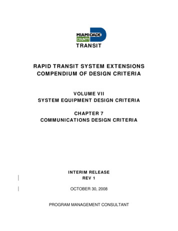
1804IEEE SENSORS JOURNAL, VOL. 11, NO. 9, SEPTEMBER 2011of using JTAG is the reconfiguration time (JTAG is serial, whileSelect Map is parallel).Regarding the node descriptors and state variable, a uniquecode has been assigned to each HW configuration that allowsthe identification of what processing, interface and/or sensingconfigurations are currently loaded in the FPGA. This code canbe read and retransmitted trough the network by the microcontroller.On top of this, the defined node control is quite simple, and itis in charge of receiving and/or sending new SW programs andHW configurations through the network, and loading them inthe C program memory.Regarding network data transmissions, a ZigBee communication module has been used and several tests have been done.Evaluation results can be found in Section V.IV. PARTIAL RUNTIME RECONFIGURABLE SYSTEM FOR WSNThe main advantage of exploiting partial reconfiguration inembedded devices, like WSN nodes, apart from the possibilityof changing part of the configuration in runtime, is that partialconfiguration files are much smaller than complete ones, andthis produces lower memory and bandwidth requirements (thiswill be demonstrated in the results Section V).In order to design a partial runtime reconfigurable system,the FPGA array is divided into reconfigurable and fixed regions.The resulting architectural division is usually called FPGAstructure, resource arrangement or partitioning [24]. In thispaper, the FPGA partial reconfigurable system has been builtbased on Virtual Architectures (VAs) that integrate both theresource division and the on-chip communications (the on-chipinterconnection of the different FPGA regions). This sectiongoes briefly through the main general steps for designing VAs,presented in [25], particularized to the target Spartan 3 FPGA(the one available in the Cookie sensor node) and, after that,the workflow used for the reconfiguration process is described.The first aspect to be taken into account for VAs is the modeland the reconfiguration granularity that are going to be supported. VA models can be one dimensional (1D) or two dimensional (2D). Partial reconfiguration in Virtex II-based architectures (including Spartan 3 FPGAs) is frame-based [26],where entire columns of logic elements are reconfigured. Thus,1D-based VAs are well suited. In order to facilitate the reconfiguration process of the system, the reconfiguration granularityselected is coarse grain, since a reconfiguration implies a full IPCore (Intellectual Property Core) to be loaded in the FPGA. Inthe context of reconfigurable systems, these cores represent already placed and routed designs (partial configuration files) andare referred as hard cores [27].The next step is to analyze the FPGA structure in order tocover the requirements of granularity and architecture model.The structure of the Spartan 3 FPGA is quite regular comparedto other FPGAs (Virtex II for instance). Therefore, the fixed areaof the FPGA occupies the leftmost and rightmost sides of theFPGA array, spanning the area enclosed between the left/rightIOs and the embedded memory columns, marked with blackrectangles in Fig. 4. The fixed area on the left side is used to access the external microcontroller, while the right side fixed areais used to access the node sensors (see Fig. 4). The middle FPGAFig. 4. Sensor node Spartan 3 FPGA Virtual Architecture (VA)—schematicview. The VA is composed of three slots with different width and a pipeline likeon-chip communication build by three types of bus macros.section that is enclosed between the two memory columns has avery regular structure, and is defined as the reconfigurable area.This area is divided into Slots. A slot is defined as a group ofFPGA Configuration Logic Block (CLB) columns. CLBs arethe main reconfigurable components. Each CLB is composedof four LookUp Tables (LUTs).In the target Spartan 3 FPGA (XC3S200), the resulting reconfigurable area spans throughout 16 CLB columns, with 24CLB rows. A pipeline-like triple slot distribution, where eachslot has a special function, has been selected. Runtime reconfiguration support applies [28] to three different functions: sensorsinterface, reconfigurable coprocessor and C-to-FPGA communication, and three different slot widths have been definedfor them, which are 2, 8, and 6 slots, respectively, according togeneric core size estimations. Slot 0 defines the communicationwith the microcontroller (microcontroller interface, referencedas uCIF in Fig. 4), slot 1 is used to allocate the reconfigurablecoprocessor (CP in the figure) and finally, in slot 2, the sensorinterface control (SIF) is allocated.An important aspect in virtual architectures is the on-chipcommunication. In the presented approach, each slot and/orfixed region is connected to the neighboring areas to form thepipeline. This connection is done using special communicationstructures called Bus Macros. All signals that have to cross theslot boundaries require a Bus Macro [26]. Apart from the unidirectional Bus Macros, provided by Xilinx, two other bus macrostructures have been designed. First, a bidirectional macro thatpasses four data bits from left to right and four bits from rightto left. The second type is also a bidirectional macro, but it isused to cross the mentioned Block RAM/Multipliers columns(BRAM/MUL column in Fig. 4). In some cases, a hard coreneeds access to such embedded resources. In the presented VA,this can be done by hard cores loaded in either slot 2 or slot 0.Once all the previous VA design considerations have been setup, the FPGA VA is defined by a set of files that result from thedesign process: i) a user constraint file (.ucf file) that mainly defines slots positions and boundaries and ii) the communication
KRASTEVA et al.: EMBEDDED RUNTIME RECONFIGURABLE NODES FOR WIRELESS SENSOR NETWORKS APPLICATIONS1805already described hard core design. After that, independentlyfrom the method used to generate partial configuration files, thenext step is to use a JTAG FPGA programming tool (iMPACTfor Xilinx FPGAs) to generate the required binary formattedboundary scan configuration file. After that, the next step of theworkflow is to send new configurations through the network to atarget node, where they are saved in a local memory and partialreconfiguration is performed.If the target FPGA is not a Xilinx one, then, a tool calledsvf2xsvf [29] has to be used to generate complete configurationfiles, but partial reconfiguration is not possible.V. RECONFIGURABLE SYSTEM EVALUATION: PARAMETERSDEFINITION, TESTS, AND RESULTSFig. 5. Runtime WSN node partial reconfiguration working flow. The flow isused to generate and send new HW configuration to the FPGA included in the“mote” node.macros used to build the on-chip communications, that are provided as relatively placed macros (.nmc files).Once the VA to be used has been selected (several VAs canbe defined for a single FPGA) and the related definition filesidentified, hard cores for the target system can be designed.This process can be done with a variety of
1800 IEEE SENSORS JOURNAL, VOL. 11, NO. 9, SEPTEMBER 2011 Embedded Runtime Reconfigurable Nodes for Wireless Sensor Networks Applications Yana Esteves Krasteva, Jorge Portilla, Eduardo de la Torre, and Teresa Riesgo Abstract—The use of reconfigurable hardware (HW) can im-pr