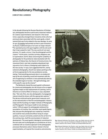
Transcription
e.sA/Va--s oboa#CHLORINE-BASED PLASMA ETCHING OF GaN l*, a m*&s** 3,&*R. J,, Shul,* R. D. Brigs: S. J. Pearton) C. B. Vartuli) C. R. Abernathy) J. W. Lee,"C. Constantine: and C. Baratt's m--4?- 0O c2"Sandia National Laboratories, Albuquerque, NM 87185-0603 L G'*z. -bUniversityof Florida, Department of Materials Science and Engineering, Gainesville, FL 32611'Plasma-Them, Inc., St. Petersburg, FL 33716Co/uF -96 /aoa-- 5)-**,,f4REC El VEDJMAl9 9997The wide band gapnitride materials continue to generate interest in the s e m i c o n d a r s T I- - group-IIt-ABSTRACTcommunity with the fabricition of green, blue, and ultraviolit light emitting diodes (LEDs), bluelasers, and high temperature transistors. Realization of more advanced devices requires patterntransfer processes which are well controlled, smooth, highly anisotropic and have etch ratesexceeding 0.5 pdmin. The utilization of high-density chlorine-based plasmas including electroncyclotron resonance (ECR) and inductively coupled plasma (ICP) systems has resulted inimproved GaN etch quality over more conventional reactive ion etch (RIE) systems.INTRODUCTIONInterest in GaN and related group-Ill nitride materials continues to grow as demonstrations ofblue, green, and W LEDs, blue lasers, and high temperature transistors are rep rted.'' Commercially available LEDs and advances in device fabrication may be attributed to recentprogress in material growth technology. Although further improvements in material properties canbe expected, enhanced device performance can only be obtained with improved process capabilitiesincluding dry etching. Laser facet fabrication is especially dependent upon dry etch pattern transfersince the majority of epitaxially grown group-III nitrides is on sapphire substrates which inhibitscleaving the sample with reasonable yield.The importance of dry etch development for the group-III nitrides is further accentuated by thefact that they resist etching in standard, room temperature wet chemical etchants. These materialsare chemically inert and have strong bond energies as compared to other compoundsemiconductors. GaN has a bond energy of 8.92 eV/atom, InN 7.72 eV/atom, and AlN 11.52eV/atom as compared to GaAs which has a bond energy of 6.52 eV/atom. Therefore, essentiallyall device patterning has been accomplished using dry etching technology. For example,commercially available LEDs from Nichia are fabricated using a C4-based reactive ion etch (RIE)to expose the n-layer of the heterostructure? Also, the first GaN-based laser diode was fabricatedusing R E to form the laser facets! The etched sidewalls were somewhat rough and may havecontributed to scattering loss and a high lasing threshold, thus demonstratmg the need forimproved dry etch processes.With the recent emphasis placed on the development of dry etch processes for the group-IIInitrides, perhaps the most crucial advancement has been the utilization of high-density plasmas.Plasma etching of GaN has been reported using several dry etch techniques including R E , electroncyclotron resonance (ECR), inductively coupled plasma (ICP), magnetron reactive ion etch(MRIE) and chemically assisted ion beam etching (CAJBE). .Using RE,GaN etch rates as highas 650 bmni have been reported at dc-biases of -400 V. 0-13 Under similar dc-bias conditions,high-density plasmas and ion beam etch systems typically yield higher etch rates than RIE etchesdue to ion densities which are 2 to 4 orders of magnitude greater. Etch profdes also tend to bemore anisotropic due to lower process pressures which results in less collisional scattering of theplasma s ecies. GaN etch rates have been reported up to 1.3 pdrnin at -150 V dc-bias in anECR,14-2P3500&min at -100 V dc-bias in a MF3E,23 2100 A/& at -500 V in a CAIBE,24 and6875 &min at -280 V dc-bias in an ICP.z-26 GaN has also been etched using low energy electron'
DISCLAIMERPortions of this document m y be illegiblein electronic image products. Images areproduced from the best available originaldocument.
DECLAIMERThis report was prepared as an account of work sponsored by an agency of the UnitedStates Government. Neither the United States Government nor any agency &ereof, norany of their employees, make any warranty,express or implied,or amrmes any legal liability or mpomiiIity for the accuracy, completeness, or usefulness of any information, apparatus,product, or process disdosed, or represents that its use would not infringe privatelyowned rights. Reference herein to any specific commercial product, process, or service bytrade name, trademark, manufacturer, o r otherwise does not necessanly'constitute orimply its endorsement, recammendation, or favoring by the United States Government orany agency thereof. The views and opinions of authors expressed herein do not necessarily state or reflect those of the UNted States Government or any agency thereof.
L.enhanced etching (LE4) at -2500 kmni in C1, at 100 C and 0 V dc-bias." In this paper, wecompare ECR and ICP etch results for GaN in C12- and BC1,-based plasmas. GaN etch ratesobtained in an ECR and ICP will also be compared to RIE results in several plasma chemistries.EXPERIMENT*The GaN films etched in this study were grown by one of three techniques; metal organicmolecular beam epitaxy (MO-MBE), radio-frequency-MBE (rf-MBE), or metal organic chemicalvapor deposition (MOCVD). The MO-MBE GaN films were grown at 925 C. on either GaAs orA120,'substratesin an Intevac Gen 11system described previously?* The group-III source wastriethylgallium and the atomic nitrogen was formed in an ECR Wavemat source operating at 200 Wforward power. The rf-MBE GaN film was grown in a commercial hBE system equipped with aconventional Ga effusion cell and a rf plasma source to supply atomic nitrogen durigg growth.The epitaxial layers were grown on a n" GaAs substrate. After deposition of a 5000 A Sn-dopedGaAs buffer layer, growth was interrupted while the substrate temperature was stabilized at 620 C.The GaN epi-layer was comprised primarily of the cubic phase. The MOCVD GaN film wasapproximately 1.8 pm thick and was grown on a c-plane sapphire substrate in a multiwafer rotatingdisk reactor at 1040 C with a 20 nm GaN buffer layer grown at 530"C?9The ECR plasma reactor used in this study was a load-locked Plasma-Therm SLR 770 etchsystem with a low profile Astex 4400 ECR source in which the upper magnet was operated at 165A. Energetic ion bombardment was provided by superimposing an rf-bias (13.56 MHz) on thesample. Etch gases were introduced through an annular ring into the chamber just below the quartzwindow. To minimize field divergence and to optimize plasma uniformity and ion density acrossthe chamber, an external secondary collimating magnet was located on the same plane as thesample and was run at 25 A. Plasma uniformity was' further enhanced by a series of externalpermanent rare-earth magnets located between the microwave cavity and the sample.ICP etching offers an attractive alternative high-density dry etching technique. The generalbelief is that ICP sources are easier to scale-up than ECR sources and are more economical in termsof cost and power requirements. ICP does not require the electromagnets or waveguidingtechnology necessary in ECR. Additionally, automatic tuning technolo,oy is much more advancedfor rf plasmas than for microwave discharges. ICP plasmas are formed in a dielectric vesselencircled by an inductive coil into which rf-power is applied. A strong magnetic field is induced inthe center of the chamber which generates a high-density plasma due to the circular region of theelectric field that exists concentric to the coil. At low pressures (5 10 mTorr), the plasma diffusesfrom the generation region and drifts to the substrate at relatively low ion energy. Thus, ICP'etching is expected to produce low damage while achieving high etch rates. Anisotropic profilesare obtained by superimposing a rf-bias on the sample to independently control ion energy. Inorder to study ICP, the ECR source and chamber were removed from the SLR 770 etch systemand replaced with a Plasma-Therm ICP source. The ICP reactor used in this study was acylindrical coil configuration with an alumina vessel encircled by a three-turn inductive coil intowhich 2 MHz rf-power was applied. Identical to the ECR, energetic ion bombardment wasprovided by superimposing an rf-bias (13.56 MHz) on the sample and etch gases were introducedthrough an annular region at the top of the chamber. The R E plasma used in this study wasgenerated by a 13.56 MHz rf-power supply in the ECR chamber configuration discussed abovewith the ECR source power turned off.All samples were mounted using vacuum grease on an anodized Al carrier that was clamped tothe cathode and cooled with He gas. Samples were patterned using Az 4330 photoresist. Etchrates were calculated from the depth of etched features measured with a D e M stylus profdometer2after the photoresist was removed with an acetone spray. Each sample was approximately 1 cmand depth measurements were taken at a minimum of three positions. Standard deviation of theetch depth across the sample was nominally less than k 10% with run-to-run variation less than k10%: The gas phase chemistry for several plasmas was studied using a quadrupole massspectrometer (QMS) or an optical emission spectrometer (OES). Surface morphology, anisotropy,and sidewall undercutting were evaluated with a scanning electron microscope (SEM). The rootmean-square (rms) surface roughness was quanflied using a Digital Instruments Dimension 3000
atomic force microscope (AFM) system operating in tapping mode with Si tips. Auger electronsp’ectroscopy ( A E S ) was used to investigate the near-surface stoichiometry of GaN before and afterexposure to several plasmas.RESULTS AND DISCUSSIONSChlorine-based plasmas have been the dominant etch chemistries used for GaN and compoundsemiconductors in general due to the higher volatility of the group-III chlorides as compared to theother halogen-based plasmas. Table I shows possible etch products and their boiling points forGaN etched in.&variety of halogen- and hydrocarbon-based plasma chenktries. In a C1-basedplasma, the high volatility of GaCl, and the nitrogen based etch products implies that the etch ratesare not limited by desorption of the etch products. However, due to the strong bond energies ofthe group-ID nitrides, the initial bond breaking of the GaN which must precede the etch productformation may be the rate limiting step.,’ Faster GaN etch rates obtained in high-density plasmaetch systems (ECR, ICP, and MRIE) as compared to RIE may be attributed to a two step processdirectly related to the plasma flux. Initially the high-density plasmas increase the bond breakingmechanism allowing the etch products to form and then produce efficient sputter desorption of theetch products. This can be seen in Figure 1 where GaN etch rates are plotted as a function of rfpower for ECR, ICP, and RIE discharges. Plasma etch conditions were; 1 mTon pressure, 10sccm Cl,, 15 sccm H,, 3 sccm CH,, 10 sccm Ar, 1000 W ECR power, and 500 W ICP power.The lowest rf-power required to generate a stable RIE plasma was 50 W, whereas both ECR andICP plasmas were stable at 1 W rf-power. Independent of etch technique, the GaN etch rateincreased as the rf-power or ion energy increased due to improved sputter desorption of the etchproducts. The ECR and ICP GaN etch rates were approximately 5 to 10 times faster than thoseobtained in the R E mode due to higher plasma densities resulting in more efficient GaN bondbreaking followed by enhanced sputter desorption of the etch products. The etched surfacemorphology was evaluated and quantified using AFM as a function of plasma etch technique. Therms roughness measured for samples exposed to the plasmas were normalized to the rmsroughness for the as-grown samples since different GaN samples were used in the etch matrix.The normalized rms roughness remained relatively constant and smooth ( -3 nm) independent ofion energy and etch platform.Etch ProductsGaC1,G*3Gal3r3GaI3(CH,),GaNCl,NF,NB r3NI3NH3N2(CH,),NBoiling Point (“C)201-1000279sub 34555.7 7 1-129explodes-33-196-33Table I. Boiling points of possible GaN etch products for halogen and hydrocarbon based plasmachemistries.
300400500rf-Power (W)Figure 1. GaN etch rates as a function of rf-power as etched in ECR-, ICP-, and RE-generatedC12/H2/CH4/Arplasmas.Chlorine-based discharges usually produce fast etch rates and smooth surface morphologies forcompound semiconductors whereas CH44-basedplasma chemistries typical result in smooth etchmorphologies at much slower rates. This is unexpected based on the information in Table 1 wherethe volatility of the Ga(CH,), etch product is much higher than that for GaCI,. This demonstratesthe complexity of the etch process where redeposition, polymer formation, or gas-phase kineticscan have a significant impact on the etch rates. An example is shown in Figure 2 where GaN etchrates are plotted as a function of rf-power for CljAr and CH4/HJAr ECR- and 00000100200. .300400500rf-Power (W)Figure 2. GaN etch rates as a function of rf-Power for ECR- and -generatedCH,/H,/Ar plasmas.CIjAr and
plasmas. These experiments were performed in the same chamber with either 1000 or 0 W ofapplied ECR power. The pressure was held constant at 1.5 mTorr and the plasma chemistry was 5sccm Cl,/lO sccm Ar or 5 sccm CH4/15 sccm H,/10 sccm Ar. GaN etch rates were si@icantlyfaster in CvAr possibly due to more efficient sputter desorption of the GaCl, etch products ascompared to Ga(CH,),. CH4/H,. plasmas may also initiate redeposition or polymer formation onthe etched surfaces thereby reducing the etch rates. Faster GaN etch rates in the high-density ECRwere attributed to enhanced GaN bond breaking and sputter desorption of the etch products.Although fast GaN etch rates have been observed in chlorine-based plasmas, the source ofreactive C1 as well as the use of additive gases have not been discussed. Unless otherwise noted,the following plasma conditions remained constant: ECR; 1mTorr, 850 W ECR power, 150 W rfPower with corresponding dc-biases of -170 to -210 V, and 30 sccm total flow with 5 sccm Ar andICP; 2 mTorr, 500 W ICP power, 95 to 115 W rf-Power with a constant dc-bias of -250 If: 10 V,and 30 sccm total flow with 5 sccm Ar. Samples etched in the ECR were grown by MO-MBEwhereas samples etched in the ICP were grown by M O O . In Figure 3, GaN etch rates areshown as a function of %H, concentration for ECR- and ICP-generated Cl&/Ar plasmas. GaNetch rates in the ECR and ICP increased slightly as H, was initially added to the ClJAr plasma(10% &)implying a reactant limited regime. Using quadrupole mass spectrometry (QMS) in theECR discharge, the C1 concentration (indicated by d e 35 peak intensity) remained relativelyconstant at 10% &.As the concentration was increased further, the C1 concentration decreasedand the HCl concentration increased as the GaN etch rates decreased in both plasmas, presumablydue to the consumption of reactive C1 by hydrogen. In Figure 4, the rms roughness is plotted as afunction of %H, for the ECR and ICP plasmas. The m s roughness for the as-grown GaNsamples etched in the ECR was 6.4 k 0.5 nm and 3.5 k 0.2 nm for samples etched in the ICP.The rms roughness for GaN etched in the ECR increased as the %H, increased from 0 to 10 andthen decreased as the &concentrationwas increased further. The roughest surface was observedat 10% H, where the etch rate was greatest. The rms-roughness for samples etched in the ICPwere less than 1 nm except for the pure Cl, plasma where the rms roughness was 41 nm.50001ncT400011112040608011-3000 2000-tloo0" 0100% H, Concentration in Cl,/H, PlasmaFigure 3. GaN etch rates as a function of %& for ECR- and ICP-generated Cl,/H.JAr plasmas.
80,I1IIECR As-grown rms 6.4 nmICP As-grown rms 3.5 nmEnIIE:vE0120140160%H2 in C12/H2Plasma180I100Figure 4. GaN rms-roughness as a function of %H, for ECR- and ICP-generated C124/Arplasmas.GaN etch profiles showed a strong dependence on the %H, in the C m / A r ECR plasma(Figures 5a - c). The etched surface was quite rough (Figure 5a) in the CLJ& plasma possibly dueto preferential removal of the GaCl, etch products or micromasking of the surface. The footobserved at the edge of the etched feature may be attributed to mask-edge erosion due to theaggressive attack of photoresist by reactive C1. As the H,concentration was increased to 20%, theetch became smooth and very anisotropic (Figure 5b). However, the SEM micrograph showed alower density of surface roughness near the etched feature than AFM images scanned in open 10 x10 pm areas. This may be attributed to a proximity effect of the etch where redeposition ormicromasking was worse in open areas. It may also explain the smooth etch observed in Figure5b where the ms roughness measured in the field was approximately 21 nm. At 60% H,, the etchremained smooth and anisotropic with a slight foot at the base of the feature (Figure 5c). For GaNsamples etched in the CyrYAr ICP-generated plasma (Figures 5d-f), the features were anisotropicand smooth independent of %H,.Smooth GaN etched surfaces were observed in a pure C1, ICPplasma (Figure 5d) where the rms-roughness was 40 nm possibly due to proximity effects.In Figure 6, BCl, was substituted for Cl, and was used to etch GaN in both the ECR and ICPreactor. The increase in etch rate observed at 10% H, concentration in the ECR-generated BCl,plasma correlated with an increase in the reactive C1 concentration as observed by QMS. As the H,concentration was increased further, the C1 concentration decreased, the HC1 concentrationincreased, and the GaN etch rates decreased due to the consumption of reactive C1 by hydrogen.In the ICP reactor the GaN etch rates were quite slow and decreased as hydrogen was added to theplasma up to 80% where a slight increase was observed. The GaN etch rates were consistentlyfaster in the C1,-based plasmas as compared to BCl, due to the generation of higher concentrationsof reactive C1.In Figure 7, GaN etch rates are shown for ECR-generated C&/sF6/& and BCl,/SF,/Arplasmas as a function of %SF,. With the substitution of SF, for H, in the Cl,-based plasma, theGaN etch rates were typically a factor of 2 slower. As the concentration of SF, was increased, theetch rate decreased up to 30% SF, followed by a slight increase at 40%. As the %SF, wasincreased from 0 to 20, the C1 concentration ( d e 35) decreased but remained si,pificant; fasterGaN etching at 20% SF, might be expected based on the C1 concentration alone. However,formation of SC1 ( d e 67) was observed at 20% SF6 which may be responsible for the reducedGaN etch rate due to consumption of the reactive C1 by S. At 30 and 40% SF,, the C1 . .-
ECR(a)ICP(d)(e (0Figure 5. SEM micrographs of GaN samples etched in either an ECR or ICP CI,,/H,/Ar plasma at(a, d) 0% & ,(b, e) 20% H,, and (c, f ) 60% &. The photoresist mask has been removed.eEfi.e31500Q)2Y1000500Figure 6. GaN etch rates as a function of %%for ECR- and ICP-generated BC1,M Arplasmas.
4000.-E:E5A1a,2c3000200010000 ’101101I1I20304050%SF6ConcentrationFigure 7. GaN etch rates as a function of %SF, concentration for ClJSF,/Ar and BCl,/SF,/Arplasmas.-concentration was greatly reduced and slow GaN etch rates resulted. The opposite trend wasobserved for BCl,, where the GaN etch rates were significantly greater when SF, was substitutedfor %. The GaN etch rate increased up to 30% SF, and then decreased sharply at 40% SF,. TheC1 concentration ( d e 35) also increased as the SF, increased to 30% and then decreased at 40%.As with the Ch-based plasma, there appeared to be a competitive reaction of sulfur with chlorine asthe SCl concentration increased above 30% SF,. Under most etch conditions, the trend of the C1concentration correlated with the trends observed for the GaN etch rates.Auger spectra were taken to determine the near-surface stoichiometry of GaN followingexposure to ECR-generated cl,4/Ar, Cl,/sF,/Ar, B C l , W k , and BC1,/SF6/k plasmas. TheAuger spectrum for the as-grown GaN showed a Ga:N ratio of 1.5 with normal amounts ofadventitious carbon and native oxide on the GaN surface. In general, the Ga:N ratio increased asthe %H,or %SF, concentration increased in either BCl, or C12 These trends implied that the GaNfilm was being depleted of N perhaps due to preferential chemical etching of the N atoms with theaddition of H,or SF, to the plasma.In the ICP reactor, GaN etch rates were obtained for Clfl,/Ar and BCl,/NJAr plasmas.Figure 8 shows the GaN etch rates as a function of %N, concentration in both C1, and BCl,. Asthe %N, concentration increased in the Cl, plasmas, the GaN etch rates decreased due to lessavailable reactive Cl., However, in the’BC1, plasmas the GaN etch rates increased signifcantly upto 40% N, and then decreased as more N, was added. This trend is similar to that observed inECR and ICP etching of GaAs, GaP, and In-containing materials?**32 Ren et al. observed peaketch rates for In-containing materials in an ECR plasma at 75% BC1,- 25% N,. As N, was addedto the BCI, plasma, Ren observed maximum emission intensity for atomic and molecular C1 at 75%BCl, using OES. Correspondingly, the BCI, intensity decreased and a BN emission line appeared.It was suggested that N, enhanced the dissociation of BCl, rksulthg in higher concentrations ofreactive C1 and C1 ions and higher etch rates. This may explain the faster GaN etch rates observedfrom 20 to 60% N, in BCl,/Ar in this study, however.higher concentrations of reactive C1 and BNemission were not observed using OES in the ICP.
nc.f5I2\b)Y0204060% N2 Concentration80100Figure 8. GaN etch rates as a function of %N, concentration for C14N2/Arand BC1,/N2/Ar ICPgenerated plasmas.Additional halogen-containing plasmas have been used to etch GaN including ICl/Ar andlBr/Ar. In Figure 9, GaN etch rates are shown as a function of rf-Power in an ECR plasma. Etchconditions were; 1.5 mTorr pressure, 1000W ECR power, 4 sccm ICMBr, 'and 4 sccm Ar. TheGaN etch rates increased with increasing rf-Power (sputter desorption) at similar rates up to 150W, however at 250 W rf-power, the GaN etch rate in ICl/Ar increased to 1.3 @min whereasthe IBr etch rate decreased slightly. This is the fastest etch rate reported to date for GaN. Nearsurface Auger electron spectroscopy (AES)showed no loss of N in the Ga:N ratio at 50100J50200250300&Power (W)Figure 9. GaN etch rate as a function of rf-Power for ECR- and RIE-generated ICl/Ar and lBr//uplasmas.
rf-powers. The high volatility of the GaI, etch products may have increased the chemical etchmechanism of the Ga and thereby minimized preferential loss of the lighter N atoms maintainingthe stoichiometry of the as-grownSince several GaN samples were used in this study, it is important to identify any etchdependence on growth technique. In Figure 10, GaN ECR etch rates are shown as a function ofrf- power for samples grown by MO-MBE, rf-MBE, and MOCVD. The ECR plasma conditionswere; 2 mTorr pressure, 22.5 sccm Cl,, 2.5 sccm H,, 5 sccm Ar, 30 C electrode temperature,1000 W microwave power, and rf-powers ranging from 1 to 450 W with.a corresponding dc-bias.range of-25 to -275 .25”T-G&l sSp1es’were etched simultaneously. As the rf-power wasincreased the GaN etch rates increased due to higher ion energies and improvGd sputter desorptionefficiency, independent of growth technique. Etch rates approaching 9000 Nmin were obtainedfor the MO-MBE and rf-MBE GaN samples at 450 W rf-power (- -275 V dc-bias). We observeda trend where the MO-MBE GaN etched faster than the rf-MBE GaN which was faster than theMOCVD GaN. Faster etch rates correlated with higher rms roughness for the as-grown GaNsamples. The nns-roughness for the as-grown GaN samples were 19.38 rf: 0.44 nm for MOMBE, 3.12 rf: 0.84 nm for rf-MBE, and 1.76 0.29 nm for MOCVD.Figure 11 shows a SEM micrograph of MOCVD grown GaN etched in a Cl,E&/Ar ICPgenerated plasma. The GaN was overetched by approximately 15%. The plasma conditions were;5 mTorr pressure, 500 W ICP power, 22.5 sccm Cl,, 2.5 sccm H,, 5 sccm Ar, 25 C electrodetemperature, and 150 W rf-power with aocorresponding dc-bias of -280 f 1OV. Under theseconditions the GaN etch rate was -6880 Nmin with highly anisotropic, smooth sidewalls. Thevertical striations observed in the sidewall were due to striations in the photoresist mask whichwere transferred into the GaN feature during the etch. The sapphire substrate was exposed duringthe overetch period and showed significant pitting possibly due to defects in the substrate orgrowth process. With optimization of the masking process, these etch parameters may yieldprofiles and sidewall smoothness which improve etched facet laser performance. Power (W)Figure 10. GaN etch rates as a function of rf-Power for MO-MBE, MOCVD, and rf-MBE grownGaN in a Cl,/HJAr ECR-generated plasma.
Figure 11. SEM micrograph of MOCVD GaN etched in an ICP-generated CIfi/Ar plasma.CONCLUSIONSIn summary, the utilization of high-density ECR and ICP chlorine-based plasmas has resultedin high rate ( 1 pdmin), smooth, anisotropic etching of GaN. The source of reactive C1 (C12,BCI,, ICI, etc.) has several effects on the etch mechanism of GaN which must be identified andunderstood. Using C12-based plasmas typically resulted in relatively high concentrations ofreactive C1 which increased the GaN etch rate. The addition of H,, N,, or SF, to Ch- or BC1,based plasmas appeared to effect the chemical removal the N atoms from the GaN or theconcentration of reactive C1 in the plasma which directly correlated to the GaN etch rate. Verysmooth pattern transfer was obtained for a wide range of plasma chemistries and conditions. Themechanism of breaking the GaN bonds appears to be critical and perhaps the rate limiting step inthe etch mechanism. High-density plasmas provide improved GaN etch results due to a two stepprocess directly related to the plasma flux. Initially .the high-density plasmas increase the bondbreaking mechanism allowing the etch products to form and then produce efficient sputterdesorption of the etch products. ICP etching of the group-III nitrides in CLJ& plasmas may yieldprofies and sidewall smoothness which improve yield and performance of etched facet lasers.Identifying plasma conditions which maintain the stoichiometry of the as-grown films andminimize plasma-induced-damage are critical to the fabrication high performance group-III nitridedevices and must be addressed.ACKNOWLEDGMENTSThe authors would like to thank P. L. Glarborg and L. Griego for their technical support. Thiswork was performed at Sandia National Laboratories supported by the U.S. Department of Energyunder contract # DE-AC04-94AL85000. Sandia is a multiprogram laboratory operated by SandiaCorporation, a Lockheed Martin Company, for the United States Department of Energy.
REFERENCESS. Nakamura, T. Mukai, M. Seno, and N. Iwasu, Jpn. J. Appl. Phys. 31, L139 (1992).H. Amano, M. Kito, K. Hiramatsu, and I. Akasuki, Jpn. J. Appl. Phys. 28, L2112 (1989).S. Nakamura, T. Mukai, and M. Senoh, Appl. Phys. Lett. 64, 1687 (9194).S. Nakamura, M. Senoh, S. Nagahama, N. Iwasa, T. Yamada, T. Matsushito, H. Kiyoku,and U. Sugimoto, Jap. J:Appl. Phys. 35, L74 (1996).5 . J. C. Zolper,’R J. Shul, A. G. Baca, R. G. Wilson, S. J: Pearton, R. A. Stall, Appl. Phys., Le.tts. 68,2273 (1996).6. S. Strite and H. Morkoc, J. Vac. Sci. Technol. B 10, 1237 (1992).7;A. Kahn, J. N. Kuzina, J: M. Van Hove, D. T. Olson, S. Krishnankutty, and R. M.Kolbas, Appl. Phys. Lett. 58, 526 (1991).8. T. Marsuoka, T. Sasaki, and A.‘ Katsui, Optoelectronic Devices and Technologies 5 , 53(1990).9. M. A. Khan, A. Bhattarai, J. N. Kuznia, and D. T. Olson, Appl. Phys. Lett. 63, 1214 (1993).10. I. Adesida, A. Mahajan, E. Andideh, M. Asif Khan, D. T. Olsen, and J. N. Kuznia, Appl.Phys. Lett. 63, 2777.11. M. E.‘Lin, Z. F. Zan, Z. Ma. L. H. Allen, and H. Morkoc, Appl. Phys. Lett. 64, 887(1994).12. A. T. Ping, I. Adesida, M. Asif Khan, and J. N. Kuznia, Electron. Lett. 30, 1895 (1994).13. H. Lee, D. B. Oberman, and J. S. Harris, Jr., J. Electron. Mat. 25, 835 (1996).14. C. B. Vartuli, S. J. Pearton, J. W. Lee, J. Hong, J. D. MacKenzie, C. R. Abernathy, and R.J. Shul, Appl. Phys. Lett. 69, 1426 (1996).15. C. B. Vartuli, S. J. Pearton, J. W. Lee, J. D. MacKenzie, C. R. Abernathy, and R. J. Shul,J. Vac. Sci. and Technol A, in press, (1997).16. C. B. Vartuli, J. D. MacKenzie, J. W. Lee, C. R. Abemathy, S. J. Pearton, and R. J. Shul,J. Appl. Phys. 80, 3705 (1996).17. S. J. Pearton, C. R. Abernathy, F. Ren, J. R. Lothian, P. W. Wisk, A. Katz, and C.Constantine, Semicond. Sci. Technol. 8, 3 10 (1993).18. S. J. Pearton, C. R. Abernathy, and F. Ren, Appl. Phys. Lett. 64,2294 (1994).19. S. J. Pearton, C. R. Abernathy, and F. Ren, Appl. Phys. Lett. 64, 3643 (1994).20. R. J. Shul, S. P Kilcoyne, M. Hagerott Crawford, J. E. Parmeter, C. B. Vartuli, C. R.Abernathy, and S. J. Pearton, Appl. Phys. Lett. 66, 1761 (1995).21. L. Zhang, J. Ramer, J. Brown, K. Zheng, L. F. Lester, and S. D. Hersee, Appl. Phys. Lett.68, 367 (1996).22. R. J. Shul, A. J. Howard, S. J. Pearton, C. R. Abernathy, C. B. Vartuli, P. A. Barnes, and .M. J. Bozack, J. Vac. Sci. Technol. B13, 2016 (1995).23. G. F. McLane, L. Casas, S. J. Pearton, and C. R. Abernathy, Appl. Phys. Lett. 66, 3328(1995).24. I. Adesida, A. T. Ping, C. Youtsey, T. Dow, M. Asif Khan, D. T. Olson, and J. N. Kuzina,.Appl. Phys. Lett 65, 889 (1994).25. R. J. Shul, G. B. McClellan, S. J. Pearton, C. R. Abernathy, C. Constantine, and C. Barratt,Electron. Lett. 32, 1408 (1996).26. R. J.Shul, G. B. McClellan, S. A. Casalnuovo, D. J. Rieger, S. J.
commercially available LEDs from Nichia are fabricated using a C4-based reactive ion etch (RIE) to expose the n-layer of the heterostructure? Also, the first GaN-based laser diode was fabricated using RE to form the laser facets