Transcription
By Jennifer HeathcoteThis article is the third installment in a three-part series designed toconsolidate key principles and technical information regarding the scienceand engineering behind UV-LEDs. If you have not read “Part I—Operationand Measurement” (July/August 2010) or “Part II—Curing Systems” (Sept/Oct2010), you may want to do so before continuing with Part III.Light Emitting Diodes (LEDs) areengineered to produce discreteinfrared, visible or ultraviolet(UV) wavelengths when a DC voltageis applied. The type of output, overallperformance and operating efficiencyof any given die is directly relatedto its material composition and themanufacturing methods employed. Asa result, there has been a concertedIt is only with an understanding of how far thetechnology has come as well as what is involvedin producing LED emitters that one can trulyappreciate the potential of where the technologyhas yet to take us.effort for the last 60 years to identifynew semiconductive compounds,improve chip structures and optimizeprocessing techniques. Much of thisactivity has been concentrated inthe longer wavelength visible andinfrared ranges; and has directly ledto improved yield rates, lower powerconsumptions, brighter colors andincreased operating efficiencies as wellas a steady decline in unit costs.By comparison, UV-LED technologyis relatively new, and engineers anddevelopers are still hard at worktrying to understand and optimize thecore technology as well as implementreliable manufacturing methods. Thepurpose of this paper is to provide ageneral history of LED development aswell as an overview of typical processesemployed in chip production. It is onlywith an understanding of how far thetechnology has come, as well as whatis involved in producing LED emitters,that one can truly appreciate thepotential of where the technology hasyet to take us.Discovery of ElectroluminescenceJöns Jacob Berzelius (1779-1848)was a successful Swedish scientistrecognized for his great achievementsin the field of electrochemistry.His penchant for methodicalexperimentation led to his discoveryof previously unknown elements,including cerium, selenium andthorium. In 1824, while attemptingto artificially manufacture diamonds,Berzelius synthesized Silicon Carbide(SiC). Silicon Carbide is a strong andchemically inert material having lowdensity, high surface hardness andminimal thermal expansion.Seven decades after the inventionof Silicon Carbide, a Pittsburgh-basedSPRING 2011 RADTECH REPORT 43Technical PaperUV-LED Overview Part III:Diode Evolution andManufacturing
Technical PaperAmerican entrepreneur, EdwardGoodrich Acheson (1856-1931),developed a low-cost, high-volumemanufacturing process to producethe material. Acheson was granteda patent for his process in 1893 andsubsequently marketed the material tothe abrasives and grinding industriesunder the trademark of Carborundum.In the early 1900s, the Britishbased Marconi Company sent a youngelectronics engineer by the name ofHenry Joseph Round (1881-1966) toAmerica to research developmentsin radio technology. One of Round’sprojects involved the evaluation ofCarborundum and its use in earlycrystal-detector radios. Roundsubjected Silicon Carbide crystals tovarious experiments, including onesin which he applied a direct current tothe material. He noticed that whenevera current was applied, the crystalsemitted light. This was the very firstobservation of electroluminescence.Round’s findings were published inthe Feb. 9, 1907, edition of the journalElectrical World.In 1928, a Russian scientist,inventor and radio technician by thename of Oleg Losev reported his ownelectroluminescence observations.He conducted a series of experimentson Silicon Carbide rectifiers used inradio circuits and discovered thatthe light emissions could be switchedvery quickly. Losev believed thatthe phenomenon could be furtherdeveloped for use as a light relay. He iscredited with being the first individualto envision a practical application forelectroluminescence.It wasn’t until the late 1960s thatthe first LEDs made from SiliconCarbide became available. The devicesemitted a blue spectral output but hada poor 0.005% electrical-to-opticalpower-conversion efficiency. Despiteall the best efforts and technologicaladvancements, pure Silicon Carbide44 RADTECH REPORT SPRING 2011diodes emitting at 470 nm neverexceeded 0.03% efficiency. As aresult, the use of Silicon Carbide inthe production of LEDs was mostlyabandoned in the 1990s for betterperforming and more efficientcompounds. In more recent years,SiC is once again being used inconjunction with more complex alloysto produce regular and high-brightnessvisible LEDs.1Evolution of LED SemiconductorCompoundsIn the decades following thediscovery of electroluminescence,researchers identified andevaluated many naturally occurringsemiconductive materials. By the1950s, the general consensus wasthat any serious advancement inthe technology would require thedevelopment of new man-madecompounds. These compoundswould be engineered to embodyspecific electrochemical andemissive properties; operate athigher efficiencies; and consume lesspower. An entire portfolio of newmaterials was necessary with thediode performance determining whichcompounds would be used for whichapplications.Formal research and developmentprojects involving LED semiconductorsstarted in the 1950s in the labs ofRadio Corporation of America; GeneralModern versions of red LEDs.Nick Holonyak, Jr., “father” of the LightEmitting Diode.Electric; International BusinessMachines; American Telephone andTelegraph; Monsanto and HewlettPackard, as well as in the labs ofvarious universities. From theseefforts, the first infrared (870-980nm)-emitting LEDs based on GalliumArsenide (GaAs) were reported in1962. Nick Holonyak, Jr., who wasconsulting at GE, is given credit for theinvention and is affectionately knowas the “father of the light emittingdiode.” Texas Instruments became thefirst company to use a small volumeof these diodes commercially at areported price of 130 each.1 Due totechnical advancements, infraredLEDs now yield a unit price that isminiscule in comparison to what TexasInstruments initially paid. As a result,infrared LEDs are extensively usedin video games, remote controls andcommunication systems.After the initial successes withGallium Arsenide infrared LEDs,
Technical Paperdevelopment projects quickly expandedto include Aluminum Gallium Arsenide(AlGaAs) and Gallium ArsenidePhosphide (GaAsP). By 1967, thefirst visible-spectrum, red emissionswere produced by a team at IBM usingAlGaAs. IBM soon integrated red LEDsmade with GaAsP into circuit boardsand mainframe computers as status andfunction indicators. Modern versionsof the devices are shown on page 2.In the 1960s, General Electric becamethe first company to commercially sellred LEDs at a price of 260 each.1 Inan effort to reduce costs, Monsantofocused on manufacturing and openeda dedicated facility in 1968 to beginhigh-volume production.Research expanded to GalliumPhosphide (GaP) in the hopes ofmaking more efficient red and greenLEDs. AT&T utilized green LEDsin the late 1970s for backlightingtouch-tone phone keypads. Theyselected red LEDs for use as statusindicators for multiline officephones. Hewlett-Packard and TexasInstruments developed GaAsP LEDsfor the alphanumeric displays indigital calculators and watches.Monsanto continued experimentingwith various manufacturingtechniques and managed to achieveemissions in the red, orange,yellow and green spectrums. Whileelectronics applications utilizingLEDs progressively expanded, thereremained various challenges regardinglow diode efficiencies, limitedbrightness, high power consumptionand the inability to view LED emittersin direct sunlight.In a much more forward thinkingpursuit, the director of the MaterialsResearch Division at RCA wasintrigued by the possibility of a flatscreen television where red, green andblue LEDs would be instantly switchedin various combinations to create videoimages. At the time, red and greenMessage-changing highway billboard with red, green and blue high-brightness LEDs.LEDs were actively being developedfrom AlGaAs, GaAsP, GaP and GaAsP;however, the industry had not yetdetermined the optimal structure forblue emitters. Gallium Nitride (GaN)was thought to be the best candidateand in the late 1960s RCA beganworking on the development of blueLEDs made from this material. RCAmade its first observations of GaNluminescence centered at 475 nm in1971. Additional doping of the materialwith magnesium generated 430 nmblue and violet LEDs.Despite some initial success, RCA’smanagement team became discouragedby the lack of commercially viableprogress and the magnitude ofadditional research required. RCAterminated its work on Gallium Nitridein the mid-70s. Even today, 40 yearsafter RCA embarked on its quest todevelop a flat screen television madeentirely of LEDs, the dream of an allLED television is still a bit elusive.While red, green and blue LEDs arewidely used for large, electronichighway billboards and commercialsignage, LEDs are limited to indicatorlights and high-brightness backlightingin all general consumer flat screentelevisions. See photos above.LED-backlit Liquid Crystal Display (LCD)television.Fortunately for the UV-curingindustry, work on GaN was resurrectedby Japan in the 1980s. In 1989,Japanese researchers produced the firstGaN junction with magnesium dopingand in 1992 a GaN UV-LED with anefficiency of around 1% was born. TheNichia Chemical Industries Corporationin Japan has been a leading driver ofdevelopment using GaN, GaInN andGaP compounds doped with impuritiesto produce high-brightness blue, green,white and UV-LEDs. Commercially,Gallium Nitride LEDs are most widelyused for backlighting electronic devicessuch as mobile and smart phones;personal data assistants; and globalpositioning systems. High-brightnessLEDs are increasingly being used inautomotive applications; traffic andpedestrian crossing signals; backlightingof LCD and rear projection televisiondisplays; and general lighting.SPRING 2011 RADTECH REPORT 45
Technical PaperHigh-brightness LED traffic signal (left)and crossing signal (right).Development work has alsocontinued on AlGaInP high-brightnessLEDs in the rest of the visiblespectrum. Alloys of these are now thedominant materials used for highbrightness emissions in the red (625nm), orange (610 nm) and yellow(590 nm) spectral range. It should beemphasized that UV-LEDs packagedfor use in curing systems still representa very small portion of the total volumeof UV, white and high-brightness LEDs;however, since the technologies aresimilar, the design and manufacturingof UV-LED chips directly benefitsfrom improved performance andhigher volume production of whiteand high-brightness diodes. Examplesof common high-brightness LEDapplications are shownat left while variouspackages of UV-LED chipsare provided in the photosto the right.Despite the negligiblepeak irradiance of the firstUV-LED chips (1992),the discovery was asignificant breakthroughin the evolution ofsemiconductor technologyas it confirmed thatLEDs were not limitedto infrared and visiblespectrums. As is the casewith most cutting edgePackaged UV-LEDs from Integration Technology (top),technologies, it oftenNichia (bottom).takes years or decadesto transition from initialLED curing systems commerciallydiscovery to viable application. Theviable for an increasing number ofevolution of UV-LEDs has been noapplications.different. It took more than a decadeUV Process Supply and Phoseonafter the first lab-created ultravioletare credited with commercializingdiode for UV-LED systems to beginthe first UV-LED systems. Otherappearing on the market (2003).companies such as IntegrationThe early systems were not veryTechnology Limited, Lumen Dynamics,powerful and the applications wereSummit UV, Sun LLC and Clearstone,limited. Fortunately, the overallto name a few, entered the marketoutput, performance and efficienciessoon afterward. Today, the majority ofhave increased every year. Startingconventional UV system developersaround 2008, UV-LED systems beganhave embarked on some level ofgenerating sufficient UV output at aresearch or commercialization ofreasonable price point to make UVirradiators made with UV-LEDs. LargeHigh-brightness Formula One rain taillight (left) and high-brightness headlight(above) are examples of common highbrightness LED applications.46 RADTECH REPORT SPRING 2011
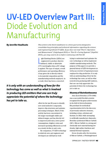
Figure 1Timeline for evolution of LEDsconductive compound, Silicon Carbide(SiC), is illustrated in Figure 1.Semiconductor ManufacturingThe spectral emission, electricalto-optical power-conversion efficiency,unit cost, quality, yield rate andlifetime hours of each die depend notonly on the substrate material, but alsoon each additional processing step andmanufacturing method employed. As aresult, significant investment has goneinto developing and controlling theproduction of LEDs.Actual manufacturing yield ratesvary significantly depending on thetype of LED. Yield rates for standardinfrared and visible LEDs haveimproved drastically over the past50 years as most of the productionissues have been resolved. Yieldrates for white and visible spectrumhigh-brightness LEDs are increasingrapidly; although, there is still room forimprovement. The current quality ofUV-LED production, unfortunately, isnot very good and much optimizationwork remains to be done. With UVLEDs, there is a significant amount ofscrap generated during production thathas a direct impact on the final die costand performance.Every single stage and step of theproduction process—from raw materialselection through to packaging—iscritical. Each has the potential tointroduce defects or foreign matter,resulting in lower efficiencies andinsufficient performance in the finaldies. As a result, numerous qualityassurance checks are performed andmost processes take place in Class1 and Class 10 clean rooms. Eachand every step of the manufacturingprocess, therefore, is a distinct andchallenging engineering and qualityimprovement project that takes years,if not decades, to perfect.An overly simplified description ofthis process can be segmented intothree parts that focus on the ingot,wafer and die. It should be notedthat there are many variations to theproduction methods described; notall steps have been included in thisdocument; and each manufacturerlikely incorporates proprietaryprocessing that is not generallyknown to the public. As a result, thefollowing sections are meant to givethe reader some general insight intoa typical LED manufacturing processand are by no means meant to be fullycomprehensive.SPRING 2011 RADTECH REPORT 47Technical Paperinvestments are being made despitethe reality that not all applications arecurrently suited for UV-LED curingand many system configurationsare still quite expensive. In lieu ofthese challenges, the overall chipand packaging technology continuesto evolve and, in time, prices andperformance will also improve. Thishas encouraged more semiconductormanufacturers, chip packagingcompanies and UV system developers toenter or consider entering the market.This increase in competition will likelyadvance the technology much furtherin a much shorter period of time.To summarize, engineers andresearch scientists have beenformulating and experimenting fornearly 60 years with an ever increasingportfolio of man-made semiconductorcompounds that emit infrared,visible and, most recently, ultravioletwavelengths. These compounds havebeen engineered to embody specificelectrochemical and emissive propertieswhile operating at increasingly higherefficiencies and consuming lesspower. Since each compound emits adifferent wavelength and/or amount ofenergy, an entire portfolio of materialsis necessary in order to producedies for various applications. Thefinal diode performance determineswhich compounds are used for whichapplications.It should be emphasized thatthe necessary research is far fromexhausted, and there are presentlycomplex alloys still in development,including GaN/SiC, GaN/Sapphire,GaN/Silicon, GaN/B–Si/pSiC, GaNGlass, GaN/ZnO, GaN/AIN, GaN/B-GaN/pAIN and GaN/Ge, to name a few. Verypreliminary research into materialsthat emit shorter wavelength UV-A,UV-B and UV-C diodes is also currentlyunderway. A timeline summarizingkey breakthroughs in developmentsince the discovery of the first semi-
Technical PaperThe IngotThe manufacture of LEDsemiconductors starts with theproduction of a long, cylindrical ingot,also called a boule. The ingot is typicallyformed to diameters of 2, 4, 6, 8 or 12inches and can be grown to any desiredlength. The material properties areuniform throughout the ingot, and thecrystalline structure contains relativelyfew impurities or contaminants. This isachieved through precision temperatureand pressure control in a cleanenvironment and by using only thehighest purity of raw materials.Formation of the ingot begins whenhigh-grade raw materials are mixedtogether in a specially designed reactorcharacteristics of the original seedmaterial (2-d). See photo at left.Before moving to the next stageof production, a diamond saw isused to remove the cone and theremaining cylindrical ingot is groundand polished.The WaferFully formed ingots.the ingot takes the shape of a conethat tapers from the seed outwardto the desired diameter (2-c). Thecrystals continue to grow in lengthas long as the process conditions areFigure 2Forming the ingotchamber as illustrated in Figure 2.When elevated temperatures andpressures are applied, the materialscombine to form a uniform moltensolution that is covered with a layerof liquid boron oxide to preventvaporization. A rod or chuck is thenlowered toward the solution (2-a). Onthe end of the chuck is a tiny, purifiedseed that contains the exact propertiesof the mixture. When the seed reachesthe solution, a chemical bond begins toform between the seed and the moltenmaterial (2-b).As the rod is rotated and withdrawnat a slow and constant rate of speed,some of the mixture begins to cooland solidify on the seed. The top of48 RADTECH REPORT SPRING 2011maintained. The applied temperaturesand pressures, as well as the rotationand extraction speed, all have a directeffect on the diameter and the qualityof the ingot. When the desired growthis reached, the seed and bonded ingotare removed from the chamber. Theresult is an ingot with all the physicalA diamond saw is used to slicethe ingot into crystalline wafers orsubstrates that are less than 250microns thick (10 mils). This isillustrated in Figure 3. After slicing,the wafer is subjected to a lappingand/or etching process in order tocarefully remove unnecessary ordamaged particles from the surface.Lapping is a physical process thatinvolves moving the wafer over a planeof liquid abrasive, while etching is achemical process intended to dissolveunwanted material. Both are used toensure a smooth surface. Next, thethickness and flatness of each wafer ismeasured, and the wafers are sortedand polished in order to improve theefficiency and quality of downstreamprocessing and make the wafers morereceptive to additional layers of semiconductive material.Any imperfections created whenthe ingot is formed and sliced or whenthe wafer is lapped, etched or polishedwill lead to a poorly functioning ornon-functioning LED. Unclean wafersalso have a negative effect on theperformance of the final diodes. Asa result, all wafers are cleaned usingFigure 3Wafers being sliced from ingot
Wafer processing—liquid phase epitaxyultrasonic or solvent-based methodsin order to remove any remaining dirt,dust or foreign matter.Next, a process known as LiquidPhase Epitaxy is used to growadditional layers of semiconductivematerial on top of each wafer. Theselayers often contain intentionallyadded impurities or dopants thatimprove the emissive characteristicsand efficiencies of the final diodes. Thedopants interfere with the crystallinestructure of the die resulting in analtered output when a voltage isapplied. All epitaxial layers have thesame crystal orientation as the ingot;however, the existence of dopantsmeans that each layer has a differentelectronic density.Each epitaxial layer is severalmicrons thick, and the process involvespassing each wafer underneathvarious reservoirs of molten materialor melt as illustrated in Figure 4. Amelt can contain one or several typesof dopants. If multiple dopants areneeded to produce the desired effect,they can either be grown on thewafer structure in sequential layersor all at once.Sometimes it is necessary to furtherincrease the quantity of dopants orintroduce new dopants into the waferstructure after the epitaxial layers aregrown. This step is often administeredusing a continuous diffusion furnaceor furnace tube where dopants areforced into the upper layer(s) usinghigh temperature gases. A photo of onesuch furnace is shown below.The next step is to add conductivemetal contacts or circuitry to thewafer. This may be done all at onceor built up sequentially by repeatingthe following photoresist and vapordeposition process several times. First,a light-sensitive, liquid material calleda “photoresist” is applied to the topsurface of the wafer while it spins.Spinning ensures that the material isevenly distributed across the entiresurface. Next, the wafer and appliedresist are baked at a low temperaturein order to harden the resist surface.A mask (also called a “reticule”)containing the metallic contactpattern is placed over the wafer. Theentire wafer is then exposed to UVlight. All exposed areas of the resistmaterial that are not blocked by thereticule cure underneath the lightand are subsequently washed awayin a developer bath. The resist thatwas under the mask remains on topof the semiconductor layers. It will beremoved in a later step.Contact metal is then evaporatedonto the wafer in the areas where theresist was removed. This is done ina high-temperature, vacuum-sealedchamber flooded with a mixture ofhydrogen and nitrogen gas. Hightemperatures are used to vaporizethe metal contact material inside thechamber. Once the metal is vaporized,the chamber conditions are adjusted inorder to condense the metal onto thewafer in the areas where the resist wasremoved. The remaining resist is thenstripped in a chemical bath leaving justthe epitaxial wafer and metal contacts.Finally, the contact pattern is annealedto the wafer in a high temperaturefurnace over a period of several hours.The end result is a chemical bondbetween the semiconductor and thecontacts. An example of a processedwafer is provided in Figure 5.Wafers pictured in front of furnace tube entrance.SPRING 2011 RADTECH REPORT 49Technical PaperFigure 4
Technical PaperFigure 5Processed waferThe Die (Chip, Diode,Semiconductor)Depending on the diameter, afully processed wafer is made up ofthousands or even tens of thousandsof individual LEDs all with the samegeneral material structure and metalliccontact pattern. Figure 6 shows oneLED die resting on the face of a U.S.penny. This single die would have beenone of many cut from a 2-, 4-, 6-, 8- or12-inch diameter wafer using a laser ordiamond saw.After the dies are extracted fromthe wafer, a forward voltage is appliedto each and every die, and the outputis measured using an integratingsphere. It is only at this time thatmanufacturers know whether theproduction process was successful.Each functioning LED is then binnedaccording to wavelength, peakirradiance, and forward voltage. Foradditional information on integratingspheres and binning, refer to “UVLED Overview Part I—Operation andMeasurement.”After the diodes are binned,they must be packaged accordingto the intended application. Thesemiconductor manufacturer will oftenpackage the dies itself before sellingthe LEDs to the market as modules.Alternatively, some semiconductormanufacturers will sell the individualdies without further packaging. In thiscase, the packaging is done directlyby the final equipment manufactureror other supplier. The packaging ofUV-LEDs was detailed in “UV-LEDOverview Part II: UV Curing Systems.”ConclusionThe evolution of LEDs has spanned187 years since the invention ofSilicon Carbide; 118 years since thecommercialization of Carborundum;104 years since the discovery ofelectroluminescence; 83 years sincethe light relay was first conceptualized;56 years since the initiative to engineersemiconductive man-made compounds;Figure 6Completed individual die shown in proportion toa U.S. penny19 years since the first UV-LED wasproduced in a lab; and eight yearssince UV-LED curing systems werefirst offered to the market. It has beena long and remarkable journey thathas involved extensive development ofpreviously unknown compounds; thecreation of diverse diode structures;and the invention and optimization ofprecision manufacturing methods.Despite all the amazingaccomplishments, this is a journeythat is still far from over. Duringthe foreseeable future, UV-LEDperformance will continue to improve.More wavelengths will becomeavailable; higher irradiances will begenerated; efficiencies will increase;lifetime hours will improve; and costswill become more attractive. Thesebreakthroughs will not necessarilyhappen overnight, but recentadvancements evaluated in thehistorical context of LED evolutionmake it hard not to be excited aboutthe technology’s future and all itspossibilities. wReferences1. Schubert, E. Fred. Light-EmittingDiodes. Cambridge, UK: CambridgeUniversity Press. 2008.2. Held, Gilbert. Introduction to LightEmitting Diode Technology andApplications. Florida, USA: AuerbachPublications. 2009.3. Light-Emitting Diode. How ProductsAre Made, Volume 1. 2006 - 2011.April 4, 2011. deLED.html4. Silicon Wafer Processing. IISME.Summer 2000. April 4, 2011.http://iisme.org/etp/Silicon WaferProcessing.pdfIndividual die50 RADTECH REPORT SPRING 2011—Jennifer Heathcote is generalmanager, North Americafor Integration Technology inChicago, Ill.
industry, work on GaN was resurrected by Japan in the 1980s. In 1989, Japanese researchers produced the first GaN junction with magnesium doping and in 1992 a GaN UV-LED with an efficiency of around 1% was born. The Nichia Chemical Industries Corporation in Japan has been a leading dr