Transcription
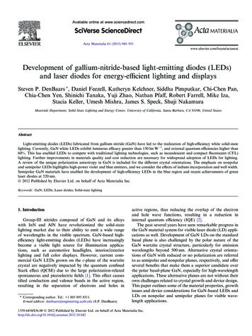
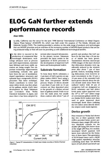
ICMOVPE IX ReportELOG GaN further extendsperformance recordsAlan MillsLa Jolla, California was the venue for the June 1998 biennial 'International Conference on Metal OrganicVapour Phase Epitaxy' (ICMOVPE IX), which was held under the auspices of The Metals, Minerals andMaterials Society (TMS). The meeting provided a window on the wide range of products and technologiesthat use MOVPE processes and an overview of the increasing number of MOVPE-based products that are being produced today or that will soon be providing us with additional technological benefits.' n the drive to succeed in theproduction of commercial blue.wavelength diode-lasers, technology advances such as processand yield improvements, extendedlaser lifetimes and more stable operation are being sought. Two important technology improvementscontributing towards this goalhave been the use of modulationdoped superlattice structures andepitaxial layer overgrowth (ELOG)processes. This latter technique,which contributes to lower substrate defect levels, was first adopted for gallium nitride (GaN) laserdevelopment by Shuji Nakamuraand co-workers from NichiaChemical Industries in Japan, andsince then it has been adopted bylseveral other research laboratories.In his plenary lecture, Nakamuraprovided the latest results in theapplication of ELOG processes tothe development of improved GaNlasers and homoepitaxial wafers.Substrate formationTo form these ELOG substrates, a2 vm layer of GaN is grown on sapphire wafers (0001C face) using adual flow, low-pressure MOVPEprocess. Stripes of silicon dioxide2 ml thick (3 tm wide on 13 tmcentres) are then deposited priorto the growth of a thicker, secondlayer of gallium nitride.Voids occurover the mask areas, but usuallythese coalesce after about 7 tm of10500CW 25 Cgrowth and produce fiat GaN surfaces by the time that a 20 ktm layer of nitride has been grown.Transmission electron microscope(TEM) images of this layer showedthat dislocation densities were significantly reduced in the windowareas after about 7 tm of layergrowth. Defects, including threading dislocations, were however almost non-existent in the 10 tm x10 tm areas of the extended GaNlayers grown directly above the silicon dioxide mask areas. These flatsurfaced wafers with 20 ktm ofovergrown GaN are designated asELOG substrates and had defectlevels many orders improved overthe 108 to 101 cm -2 defect rangeof conventional gallium nitride layers. Similar ELOG wafers were thenused to grow improved shortwavelength diode lasers (utilizingthe low defect areas directly abovethe striped oxide mask regions).400Device growthE - a00oQ.62004-5lOO2 f::LOv(D01002003004000500Current (mA)Figure 1. Typical RT characteristics of InGaN laser diodes (courtesy of Nichia ChemicalIndustries).36III-VsReview Vol.11 No. 6 1998Prior research at Nichia had shownthat two or three quantum wells(QWs) provided better power performance than a single QW, with device threshold currents for thedouble QW being 50% below thoseof the single QW.Thus, two modulation-doped InGaN quantum welllayers were selected for the formation of these lasers. This generationof ELOG-based lasers used a MQWridge guided, superlattice structurecombining more than 720 MOVPElayers of GaN,AIGaN and InGaN epi0961-1290/98/ 19.00 1998ElsevierScience Ltd.All rightsreserved.
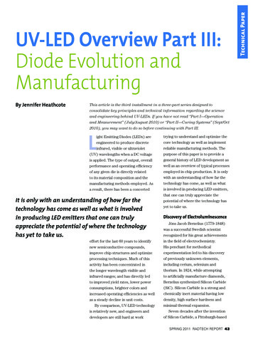
ICMO VPE IX Report150only 50% of sapphire substratelasers (30 C.W 1 versus 60 C.W 1for sapphire substrates). Heat-sinksupported ELOG wafers are expected to have even lower heatrise coefficients. By the time of theICMOVPE IX conference, these homoepitaxially grown lasers hadachieved another first: 300 hoursof operation without degradationat 50 C.At the time of writing this50 C operating lifetime n o w extends to over 500 hours.CW 2 mW 20"C100gk-500IIII10002000300040005000Time (hours)Figure 2. Operating current of ELOG laser diodes versus lifetime (courtesy of Nichia).taxy. They were fabricated on standard sapphire substrates, subsequently thinned to 70 tm.Formation of the laser structurewas completed by cleaving thewafer, half-coating the end facetswith two pairs of quarter-wave titanium dioxide/silicon dioxide mirrors (to reduce the thresholdcurrent for the evaluation devices)and by the deposition of metal contacts (nickel/gold for the p-GaN layer and titanium/aluminium for then-GaN layer).Typical room temperature characteristics of these ELOG-basedblue ( 408 rim) laser diodes areshown in Figure 1. The data include the highest reported continuous wave (CW) p o w e r output fora III-V nitride laser of 420 mW atan operating current of 490 mA.Other ELOG-based diodes supported a range of first-time achievements. The firsts include the420-mW output p o w e r per laserfacet, a demonstrated 250 hourlaser lifetime at a 50 C operatingtemperature and, at lower p o w e rlevels (2 mW at 20 C), ELOG-basedlaser diodes having lifetimes in excess of 4800 hours (Figure 2). Atthe time of writing, these operating lifetimes n o w exceed 6000hours. All of these achievementsare the best values reported todate for III-V nitride lasers. Similarlasers fabricated in the w i ndow re-gions of the ELOG substrates,rather than the mask regions, hadhigher threshold currents, whichare presently presumed to becaused by increased light scattering from the much higher levels ofscrew dislocations present in theseregions ( - 10 7 cm2).Many of these process improvements have benefited not onlylaser development but also nitridebased LED processes. Thus today'sbest light output levels for nltrideLEDs are 5 lumens per watt (I.W-1)for blue, 30 l.W] for green and 10l.W] for yellow, placing them all inthe commercial device category, either as technology leaders or serious contenders.GaN homoepitaxyIn related developments at Nichia,the thickness of the ELOG layerwas increased to 250 tm using hydride vapour phase epitaxy. Thesapphire substrate was then removed to form 'bulk' GaN wafers,which were subsequently used forMQW laser diode fabrication. Asanticipated, these wafers were easier to cleave for laser facet formation, and the homoepitaxiallygrown lasers operated at significantly lower temperatures (for agiven p o w e r output). For example,the temperature rise during operation for an unsupported laser wasReal-time monitoringReal-time process monitoring haslong been claimed as an MBEprocess advantage over MOVPEprocesses. As sensor and processtechnologies have been improvinghowever, real-time monitoring hasbecom eacceptedfor s o m eMOVPE processes. In his plenarylecture, J. Thomas Zettler from theTechnical University of Berlin,Germany, described the benefitsofReflectanceAnisotropySpectroscopy (RAS) also known asRDS(ReflectanceDifferenceSpectroscopy) for MOCVD. RASwas first described by Bellcore(Morristown, NJ, USA) over tenyears ago and it is now widely usedto follow both MBE and MOVPElayer growth processes, particularly for III-V materials.The RAS signature originates in the first threemonolayers of a surface and istherefore very indicative of surfacecomposition, atomic structure anddoping effects in the growing layers, each of which can cause significant changes in surface chargeand the reflectance signal. RASmonitoring has improved such thatit can n o w be used on standardMOVPE systems, including rotatingwafer systems and it can monitordevice growth processes. Therefore, RAS can n o w be used to readsurface stoichiometry, surface morphology, surface reconstructionstates (4x4, 2x4, 2x6 etc.), dopingeffects, and significant surfacechanges during gallium arsenideand ternary com poun d layerIIl-Vs Review Vol.11 No. 6 199837
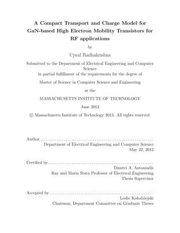
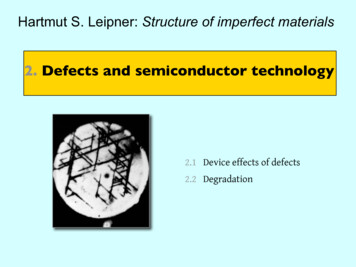
ICMO VPE IX ReportMOVPE advances in amber LEDsn addition to the leading-edgework on short wavelength GaNemitters by MOVPE processesreportedabove, theNichiaLaboratory hasrecently announced the development of highambient operating temperatureamber (590 run) LEDs. Previousamber LEDs developed at Nichiahad lower output power ( 5 mW)thancommerciallyavailableAIInGaP (aluminium indium gallium phosphide) LEDs a n d wouldnot have been accepted in thecommercial markets. However, inon-goLt!g research concurrent withthe laser developments, newly reported work on MOVPE-grownLoGaN LEDs based on the structure shown in Figure 3 has led toimproved device performance,with the potential for commercialapplications.The latest amber LEDs are single quantum well (QW) structuresMOVPE-grown on sapphire substrates under similar flow conditions to the blue lasers, but athigher pressures (1 atm). The dimensions of these LED structures(Figure 3) consist of a 300 A GaNbuffer layer, a 0.7 tm thick layer ofundoped GaN, a 3.3 gtn thick layerof n-type GaN:Si, a 400 A currentspreading layer of undoped GaN, a25 A thick active layer of undopedInGaN, a 300 A thick layer of pAIGaN:Mg and 0,2 tm p-type layerof GaN:Mg as the contact layer.Unlike previous amber InGaNLEDs, an important2.0feature in the n e w 1.8aP LEDsstructure is the inserc1.6tion of an undopedGaN layer next to the1.4active layer. This highOe resistivity layer causes,5 1.2the current to be1.0InGaN LEDsspread uniformly overo0.8the active InGaN lay. .t er.- 0.6To form the LEDw 0.4IIIII-20020406080-40lamps, the wafersAmbienttemperature( C)were etched to expose the n-GaN con- Figure 4. The output power of amber InGaN and AIInGaPtact areas and metal LEDs as a function of the ambient temperature. Output wasnormalized to 1.0 at 25 C for each LED. (Courtesy of Nichia.)c o n t a c t s similar tomoulded into lamps. The outputthose used for the lasers werepowers of these new LOGANLEDsevaporated on to the 1 and n-reand commercial amber LEDs aregions.After being cut into 350 tmshown in Figure 4, where thex 350 gm squares, the LED diepower values have been normalwere attached to lead frames andgrowth. By using the ratio betweentwo parts of the analytical spectrum, it can also be used to estimate surface temperature andchanges in temperature. Thus RASmonitoring can n o w provide avery versatile real-time analyticaltool for both the research engineerand the device manufacturer, including on-line process calibration,during the MOVPE process.In later papers, the use of RASto monitor GaAs growth condi-tions was also reported by otherlaboratories. Randall Creightonfrom Sandia National Laboratories(Albuquerque, NM, USA) used RASto define deposition rates accurately over a wide range of growthconditions. At higher trimethyl gallium (TMG) feed rates and/or lower temperature conditions, 'aninteresting' sub-linear dependenceon TMG partial pressure was observed. In this regime a lx2 reconstruction occurs on a methyliIIl-Vs Review Vol.11 No. 6 199838p-,UnUnGaN bufferSapphire subsFigure 3. The structure of amber InGaN LEDs (courtesy of Nichia Chemical Industries).group terminated arsenic-rich surface. Markus Pristovsek from theTechnical University of Berlin described the use of RAS to monitorthe homoepitaxial growth of gallium arsenide on high index surfaces. All surfaces exhibited tworeconstructions, one arsenic richand the other arsenic deficient.Simon Watkins from Simon FraserUniversity(Burnaby,BritishColumbia, Canada) reported on theextension of RAS techniques to the
ICMO VPE IX ReportTable I. The characteristics of amber InGaN and AIInGaP LEOs measured at a current of 20 mA at RTOutput power (mW)Forward voltage (V)Peak wavelength (nm)FWHM (nm)Luminous efficiency (m-lW -1)Rise time (ns)Fall time (ns)Amber InGaN LEDs1.43.359450l0Amber AIInGaP LEDs0.661.9559117820302724perature and that thetemperature dependence of the output issuperiorforthe InGaN LEDs in the100 ! j m m / n n '-20 to 80 C range.OfD.The output of the"5InGaN LEDs decreases only by 10% beOtweenroom. 80temperatureand80 C.Theyalsoshowed no degradation for up to 100060IIII1o0hours of aging (Figure02004006008005). The rise and fallAging time (hours)times for both LEDsFigure 5. Output power as a function of aging time for amber were similar, as wereInGaN LEDs operated at a forward current of 20 mA at RT.the luminous efficien(Courtesy of Nichia.)cy values at 10 l.W-1ized to unity at 25 C. The imporfor the InGaN devices and 8 I.W-1for the AIInGaP LEDs.tant device characteristics at roomtemperature are compared in TableThe spectral purity for the1, at drive currents of 20 mA andcommercial device is better thanusing typical forward voltages ofthe developmental InGaN LED 3.3 V for the InGaN devices. It can17 nm versus 50 um width at theirbe seen that the output power ofrespective FWHMs (full width atthe new InGaN LEDs is abouthalf maximum) - but this differtwice as high as that of the comence would probably not be demercial amber lamps at room temtectable by the human eye. Thelarger spread was presumed to bedue to inhomogeneities in theQW indium content. From the information presented it is probablethat the InGaN LEDs could alreadyserve practical uses for highertemperature applications and, incidentally, an advantage was alsoclaimed for the nontoxic nature ofthe InGaN on sapphire system. Asthis InGaN technology is in its early stages, considerable improvementsinperformanceareexpected; however, cost-effectivemanufacturing processeswillhave to be developed before theycould compete in the main commercial markets. With ultraviolet,blue, green and n o w amber LEDsand/or lasers, these developmentsillustrate the ever increasing rangeof light emitting products that canbe manufactured from gallium nitride MOVPE processes and formthe basis for several n e w growthmarkets. Red GaN-ba. l LEDshave also been demonstrated, buttheir performance was a long wayoff from that of the other III-VLEDs.atomic layer epitaxial growth of indium arsenide and indium phosphide layers. InAs layer growth wassimilar to that of GaAs with a selflimiting double arsenic layer beingpresent, but no evidence wasfound for a double phosphorus layer during InP layer growth.natural regular ordering such ascheetah spots and zebra stripes.Temmyo suggested that consideration of natural processes and'Turing stability' could play a "pioneering role for optical devices innew, exotic, large-mismatch" devicegrowth conditions. 120Turing stabilityIn the next series of invited talks, J.Temmyo, from NTT Laboratories(Kanagawa,Japan), discussed self-organization (ordered) versus the serfassembly of InGaAs of quantum dotsized islands. The island shapes (triangular, zigzag) on 311B surfacesvaried with indium composition atgrowth temperatures in the 700 to800 C range. The order of these islands was considered to be withinthe realm of Turing stability, as defined by the mathematician AlanTuring in 1952 for short-range autocatalysis, and was compared withInSb sensorsChristine Wang from MIT LincolnLaboratory (Lexington, MA, USA)III-Vs Review Vol.11 No. 6 199839
I C M O VPE I X Reportdescribed the growth of indium/antimony/arsenic heterostructures using MOVPE processes, whichproduced sensor performances exceeding those of MBE grown devices based on the same alloystructures. In this work TEG, TMI,TMSb and TBA were used to growGaInAsSb heterostructure layers,which are lattice matched to gallium antimonide. Devices based onthese GaSb-GalnAsSb-AICmAsSb heterostructure alloys have cutoffwavelengths in the 2 to 2.4 lainwavelength region, which correspond to black body radiation in the1100 to 1500 K temperature range(0.5 eV bandgap).The benefits of the MOVPEprocesses are the reduction ofgrowth times to about one hourfrom six hours, and the achievement of the highest quantum efficiencies and open circuit voltagesobtained to date for thermophotovoltaic devices at 2.3 gtm. Withwindow coatings, absorption efficiencies of up to 70% have been obtained. Although most of the alloysin the necessary compositionalrange are metastable, no degradation of properties was detected fordevice structures grown at rates notexceeding 5 tm per hour.This year the conference alsorecognized the rapidly growingfield of oxide film depositions byMOVPE in the invited paper presented by Bruce Wessels fromNorthwestern University, IL, USA.Spurred on by the silicon devicedemand for high dielectric constant materials and new barrier layers, he reported on the successfulepitaxial deposition of barium titanate ferroelectric oxides for future multi-gigabit DRAMs anderbium doped titanates for waveguides.Thin film electro-optic modulators have been made andferroelectric oxide thin m s showgood prospects for future optoelectronic IC devices.Germanium substratesFor many years silicon has beenIII-Vs Review Vol.11 No. 6 199840proposed as the eventual substrate of choice for the production of 'low cost' GaAs devices and the quest continues in somelaboratories. Unfortunately, thistechnology may never succeed asthe 'low cost' III-V substrate, because gallium arsenide epitaxy onsilicon appears to cost about thesame as a GaAs wafer (and because of the potential drawbacksof the large lattice mismatchwhich creates defects and processproblems).During the last few years however, a stealth operation has beenmounted by germanium to become the low cost substrate ofchoice for the MOVPE manufacture of some III-V devices. Despitethe potential theoretical problemsassociated with the growth of gallium arsenide on germanium, suchas differences in thermal expansion and crystal polarity, the use ofbuffer layers has allowed germanium to become the substrate ofchoice for III-V based space-application AlGaAs/GaAs solar cells.The benefits offered by germanium substrates are lower cost,larger sized wafers, significantlyhigher wafer strength and low defect levels (zero etch pit densities).This substitution for gallium arsenide is relatively easy to makebecause there is only a small latticemismatch (0.12%) between thetwo substrate materials, whichwould be insignificant for most device applications. Similar layergrowth technology has now beenextended to light-emitting devicesin a cooperative effort in Belgiumbetween IMEC, based in Leuven,and Union Mini re, headquarteredin Brussels. Mark D'Hondt et al. described the successful development of AIGaAs lasers and LEDs ongermanium substrates, which nowshow promise for the productionof commercial devices.Nitrides from DMHRajaram Bhat from Corning Inc(Corning, NY, USA) described thelow pressure MOVPE growth ofarsenide/nitride QWs using dimethyl hydrazine (DMH) as the nitrogen source. In this approach,the nitrides are being synthesizedfrom the low nitrogen end of therange and the active layers werewells with 99 periods of 1.7 nmGaAsN (N content --- 2.6%) and 2.5nm of GalnAsN (N content 5.4%).The intended application ofthese arsenide/nitride emitters is1.55-gtm lasers.Although the contained nitrogen levels were low (up to 5%),photoluminescence at 1.35 gtmwas obtained from GaInAsNstrained layer QWs where the nitrogen content did not exceed4.2%. Several other researchgroups also reported the growthof mixed arsenide/nitride structures from DMH sources, but theirnitrogen incorporation did not exceed 1%.In related nitride research,Daniel Friedman from NREL(Golden, CO, USA) described theDMH-sourced MOVPE growth ofGalnAsN active layers on galliumarsenide for potential solar applications. One electron volt solarcells were successfully preparedwhich, if combined into four-junction structures, would have thepotential for 46% efficienciesfrom cells under 500 suns radiation intensity.The conference location wasvery attractive and overlooked thePacific Ocean, a feature that addeda sense of tranquillity to the surroundings, a benefit for which TheMetals, Minerals and MaterialsSociety must be thanked.The conference closed with promises ofan equally distinguished locationbeing selected for the milleniumedition, still two years away.Contact" Dr Alan MillsPO Box 4098Mountain ViewCA 94040, USA.Tel: 1-650-968-2383;Fax: 1-650-968- 8416;E-mail: amills@inreach.com
GaN homoepitaxy In related developments at Nichia, the thickness of the ELOG layer was increased to 250 tm using hy- dride vapour phase epitaxy. The sapphire substrate was then re- moved to form 'bulk'