Transcription
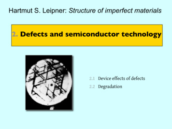
Hartmut S. Leipner: Structure of imperfect materials2. Defects and semiconductor technology2.1 Device effects of defects2.2 Degradation
2.1 Device effects of defects„Über Halbleiter sollte man nicht arbeiten, das isteine Schweinerei, wer weiß ob es überhauptHalbleiter gibt.“[Pauli 1931]hsl 2007 – Structure of imperfect materials – Epitaxy and interface defects2
The first transistor and ICTransistor as invented by Bardeen andBrattain at Bell labs, 1947hsl 2007 – Structure of imperfect materials – Epitaxy and interface defectsIntegrated circuit of J. Kilby, 19583
Cost reduction“In 1958, the year of the invention of the integratedcircuit, a single transistor sold for about 10. Today, it ispossible to buy more than 50 million transistors for thatprice.”[Kilby: 2000]hsl 2007 – Structure of imperfect materials – Epitaxy and interface defects4
Moore’s lawIn 1965 Gordon E. Moore postulated his law: The doubling of transistorsper circuit every couple of years.Intel expects that it will continue at least through the end of this decade.hsl 2007 – Structure of imperfect materials – Epitaxy and interface defects5
log (number)Moore’s lawsTimeFunctional form of key semiconductor industry business trends (Tx – transistors)The exponential expansion of the total number of transistors per chip or area againstthe time (in years) over the last half-century is known as (the original) Moore’s law.hsl 2007 – Structure of imperfect materials – Epitaxy and interface defects6
The field-effect transistor (FET)SourcenGatepDrainnStructure of a MOSFET (metal–oxide–semiconductor FET). The electrical contact tothe gate is separated from the semiconductor by a thin layer of insulator, typicallysilicon dioxide.hsl 2007 – Structure of imperfect materials – Epitaxy and interface defects7
Mobility of electrons in n-type semiconductorsMobility related to acoustic phonon interactionμn (cm2 V 1s 1)µv ! (m ) 5/3 T 3/2Mobility related to ionized donorsµD ! (m ) 1/2 ND T 3/2111 µnµv µDConductivityT (K)σ neµnMobility of electrons μn in Si[Yu, Cardona 2001]hsl 2007 – Structure of imperfect materials – Epitaxy and interface defects8
Scattering at dislocationsTwo contributions:Scattering due to the deformationpotentialLinear arrangement of charged scatteringcentersμnaType and direction of dislocations areimportant:I–U characteristics measured parallel andTperpendicular to the dislocations are differentMobility of electrons in n-type Ge before andafter plastic bending. Curve (a) was calculatedwith the space-charge cylinder model.[Seeger 1997]hsl 2007 – Structure of imperfect materials – Epitaxy and interface defects9
Electron mobility and dislocation densityRelaxed Si1 xGex, x 0.3Graded Si1 yGey, y 0 0.3Si SubstrateThickness of graded layer (µm)Effect of the grading rate in the buffer on the density of threading dislocationsand the electron mobility measured at 0.4 K. The dotted line is an extrapolationshowing that the mobility is not limited by the dislocations once their density isbelow 107 cm 2 (thickness of graded layer 0.5 µm).[Ismail 1996]hsl 2007 – Structure of imperfect materials – Epitaxy and interface defects10
Reverse current (A)Diode characteristics and dislocationsBias (V)Reverse bias I–U characteristics for InP photodiodes containing differentdislocation densities (given in cm 2)[Beam et al. 1992]hsl 2007 – Structure of imperfect materials – Epitaxy and interface defects11
Dislocations at the p–n junction Dislocations as electrically active defects cause a shortening of the junction Transport of minority carriers under reverse bias affected Energy levels of dislocations (recombination centers): source of electrical noise Dopant precipitation at dislocations: local field enhancement under reversebias, drop in reverse breakdown voltage Microplasma (high electron–hole density) formationhsl 2007 – Structure of imperfect materials – Epitaxy and interface defects12
Charged-dislocation model - -Captured majority carriersModel of Read (1957): The line charge of the dislocation is screenedby a cylindrical space charge region, i. e. in an n-type semiconductora negative dislocation is surrounded by positively charged donors.Radius of the Read cylinder:(Q charge per unit length)Smearing out of the screening cloud for T 0hsl 2007 – Structure of imperfect materials – Epitaxy and interface defects13
Influence of dislocations on the p–n junctionTop surfaceAHigh concentration zone ofphosphorus donorsBn layerCp–n junctionScheme according to Holt (1996) illustrating the absorption of the diffusing impurity(e. g. phosphorus) by dislocations and the retardation of the diffusion front. In this way,cusps in the p–n junction are produced. The magnitude of the effect depends on thedepth of the dislocation; shallower ones produce the larger effects. A and B are stronglydecorated dislocations. The impurity atmosphere at dislocation C is weaker.hsl 2007 – Structure of imperfect materials – Epitaxy and interface defects14
Defects in GaAs field-effect transistorsSourceBGateDrainn channelBSI GaAs substrateStructure of a FET. Si implantation is used for the production of the n-conductivechannel. Lateral isolation is provided by amorphization in B. The symmetrical n contacts are made of Ni/Au–Ge, the gate by Ti–Pt–Au. The drain/source–gate separationis 2 µm.hsl 2007 – Structure of imperfect materials – Epitaxy and interface defects15
Precipitates in FET structures(a)(b)LSTLSTLaser scattering tomography (LST) of precipitates (a) decorating dislocationsin the substrate and (b) in the channel between drain and gate.[Castagné et al. 1992]hsl 2007 – Structure of imperfect materials – Epitaxy and interface defects16
(a)Threshold voltage (mV)Precipitate density (cm 3)FET characteristic curvesBreakdown voltage (V)2 µm20 µm50 µmTheoryPrecipitate density (cm–3)(b)Influence of the precipitates on the breakdown voltage (a) and the threshold voltage (b)of the GaAs FET. The symbols in (b) represent different lengths of the channels.[Castagné et al. 1992]hsl 2007 – Structure of imperfect materials – Epitaxy and interface defects17
2.2 Degradation Limitation of the lifetime of semiconductor devices, especiallyoptoelectronic devicesDefect formation during operation Classification of degradation modes, recombination enhanced defect generation and motionhsl 2007 – Structure of imperfect materials – Epitaxy and interface defects18
Scheme of a laser diodeCurrentwActive zonedpedp doOpticallyroughpedn doLRadiationBasic structure of a laser diodeOptical resonator realized withthe Fabry–Perot conditionmλ 2nL(m integer number, λ wavelength,n refraction index, L resonatorlength)Mirror facePopulation inversion at thep–n junction as the lasingcondition (i. e. stimulatedemission larger than opticalabsorption)hsl 2007 – Structure of imperfect materials – Epitaxy and interface defects19
GaN laser diodeNichia blue laser diodeconsisting of a stack ofAlGaN, GaN, and InGaNlayers. The SiO2 islandsare stoppers forthreading dislocations.Top surfaceDouble heterostructure1 µmGaNSubstrate–film interfaceAl2O3hsl 2007 – Structure of imperfect materials – Epitaxy and interface defectsTEM cross-section image ofthe layer containingthreading dislocationsTEM[Lester et al. 1995]20
Quantum efficiencyInfluence of dislocations on device efficiency1.0GaN0.80.60.4GaAs0.2GaAlAs410510GaP GaAsP610710810910Dislocation density (cm–2)Light output as a function of the dislocation density in the active region for variouslaser diodes according to Lester et al. (1995) and Sugahara et al. (1998)hsl 2007 – Structure of imperfect materials – Epitaxy and interface defects21
Light outputDegradation of light-emitting devicesTime of operationA representative degradation curve of light output versus time. The scalealong the ordinate can vary over hours to ten on thousands of hours.hsl 2007 – Structure of imperfect materials – Epitaxy and interface defects22
Formation of dark-line defectsELELMicro-electroluminescence distribution of !110"-oriented dark-line defectsin a high-power GaAs light-emitting diode of the 1980ies.hsl 2007 – Structure of imperfect materials – Epitaxy and interface defects23
Dislocations in a GaAs LED(a)EBIC21(b)CL321325 µmDislocations in a GaAs light-emitting diode in EBIC (a) and cathodoluminescence (b)images. Note the vanishing contrast in (b) for the dislocations 1 to 3.[Schreiber et al. 1984]EBIC – electron beam induced currenthsl 2007 – Structure of imperfect materials – Epitaxy and interface defects24
Dark-line defects and dislocation motionEL!100"10 µmTEMDark-line defects of a GaAlAs laser diode in the electroluminescence distributionand in a transmission electron microscope image. B denotes a threadingdislocation and A the formation of a dislocation dipole in a !100" direction. g is thediffraction vector.[Hutchinson, Dobson 1980]hsl 2007 – Structure of imperfect materials – Epitaxy and interface defects25
Growth of dark-line defectsNActive layerbScheme of the growth of a dislocation network in theactive layer of the laser device. (a) Initially, thedislocation PN with the Burgers vector b crosses thelayer; (b) climb into the active zone; (c) further climbconfined to the active zone causes elongation alongthe [100] direction.[Hutchinson, Dobson 1975]PTEMhsl 2007 – Structure of imperfect materials – Epitaxy and interface defects26
Dislocation climb in the active layer(a)(b)Two models proposed for the extension of !100" -oriented dark-line defectsin degraded optoelectronic devices via dislocation climb. (a) Model relatedto absorption of interstitials, (b) emission of vacancies.hsl 2007 – Structure of imperfect materials – Epitaxy and interface defects27
Influencing defects by carrier recombination Release of energy by recombination of excess carriers (photons, phonons) Recombination energy may be directly used for defect reactions(generation, motion, transformation) – recombination enhanced defect reaction Energy transfer can be directly an special sites on the dislocation (kinks) –recombination enhanced dislocation glide Stimulated activity of the kink migration: increase in the dislocation velocityhsl 2007 – Structure of imperfect materials – Epitaxy and interface defects28
Electron-beam-stimulated dislocation motionCLMoving dislocations near ascratch on GaAs observed bycathodoluminescence imaging[Höring et al. 2000]hsl 2007 – Structure of imperfect materials – Epitaxy and interface defects29
Recombination enhanced dislocation glideTemperature dependence of thethermal and recombination-enhanceddislocation velocity υ of polar 60 αand β dislocations in GaAs[Maeda, Takeuchi 1983]n-type GaAsτ 26 MN m 2with/without irradiationαβv (m/s)I 0.26 A m 2III 2.6 A m 21000/T (K 1)!υ υ0 τ m exp QkB T"!"Q !E ηI exp kB T(Q activation energy in the dark, I beam current density, ΔE reduction in the activation energyby the electron beam, τ stress, m stress exponent, υ0 and η prefactors)hsl 2007 – Structure of imperfect materials – Epitaxy and interface defects30
Defect structures 〈110〉-oriented dark-line defects(GaAlAs)dislocation glide enhanced by nonradiative recombination of carriers 〈100〉-oriented dark-line defects(GaAlAs)recombination-enhanced dislocation climb Dark-spot defects(InGaAsP)reaction between metal contacts and the matrix, microdefectshsl 2007 – Structure of imperfect materials – Epitaxy and interface defects31
Degradation modes Catastrophic optical damage( 1 h)Local heating at the mirror surface related to high output-power density Rapid degradation( 100 h)Formation of dark-line defects Gradual degradation(several 1000 h)Microdefects (loops, point defect clusters) Facet degradation( 10000 h)Oxidation or point defect formation at the mirror facetshsl 2007 – Structure of imperfect materials – Epitaxy and interface defects32
ReferencesJ. C. Kilby in: Handbook of semiconductor manufacturing technology, Marcel Dekker 2000.P. Y. Yu, M. Cardona: Fundamentals of Semiconductors. Berlin: Springer 2001.K. Seeger: Semiconductor Physics. Berlin: Springer 1997.K. Ismail: Sol. State Phen. 47–48, (1996) 409.E. A. Beam et al.: Semicond. Sci. Technol. A 7 (1992) 229.D. B. Holt: Scanning Microsc. 10 (1996) 1047.S. D. Lester et al.: Appl. Phys. Lett. 66 (1995) 1249.T. Sugahara et al.: Jpn. J. Appl. Phys. Pt. 2 37 (1998) L398.J. Schreiber et al. in: 6. Tagung Mikrosonde, Dresden 1984, p. 151.P. W. Hutchinson, P. S. Dobson: Phil. Mag. A 41 (1980) 601.K. Maeda, S. Takeuchi: J. Physique 44 (1983) C4/375.hsl 2007 – Structure of imperfect materials – Epitaxy and interface defects33
GaN laser diode Nichia blue laser diode consisting of a stack of AlGaN, GaN, and InGaN layers. The SiO 2 islands are stoppers for threading dislocations. Top surface Double heterostructure GaN Substrate–film interface Al 2O 3 TEM cross-section image of the layer containin


