Transcription
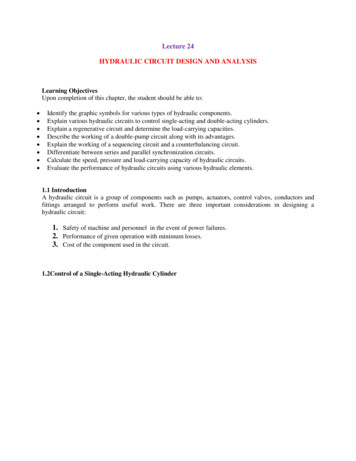
Lecture 30: Cleanroom design andcontamination controlContents1 Introduction12 Contaminant types2.1 Particles . . . . . . . . . . . . . . . .2.2 Metal ions . . . . . . . . . . . . . . .2.3 Chemicals . . . . . . . . . . . . . . .2.4 Airborne Molecular contaminants . .2.5 Contamination problems and sources2244553 Clean room design.64 Clean room materials124.1 Process water . . . . . . . . . . . . . . . . . . . . . . . . . . . 124.2 Process chemicals and gases . . . . . . . . . . . . . . . . . . . 125 Wafer-surface cleaning115IntroductionYield improvement is the biggest challenge in integrated circuit fabrication.Initially, process is focused on producing a wafer with a yielding die, i.e. a diethat works according to the IC specification. Once, that has been obtainedyield steadily increases. The limiter for yield is usually wafer contaminationin the fab. This has become even more important now, since device dimensions are currently in the nm range. Cleanroom technology is designed tominimize this contamination. Figure 1 shows two examples of particles onwafer. A particle between two metal lines can cause shorting of electricalsignals. Figure 2 shows SEM images of two types of defects that have caused1
MM5017: Electronic materials, devices, and fabricationFigure 1: Defects between (a) metal lines and (b) on the surface of a wafer.Surface defects can affect the growth of new layers while defects betweenmetal lines can cause electrical shorts. Adapted from Microchip fabrication- Peter van Zant.an open circuit and a short circuit. Particles on surfaces can cause errors inlithography by interfering with the masking process. As device dimensionsshrink, the minimum dimensions of these defect particles also shrink. Sometypical sizes of contaminants are shown in figure 3.2Contaminant typesContaminants can be divided into five main classes.2.1ParticlesCurrent device dimensions in the semiconductor industry are in the nm range.The devices are also densely packed, so that the spacing between adjacentlines are also in the nm range, see figure 1. Compared to this, human hairis approximately 100 µm in diameter and typical dust particles are 1 µm insize. Some common particle sources in the fab are1. People working in the fab2. Generated by fab equipment3. Processing chemicals2
MM5017: Electronic materials, devices, and fabricationFigure 2: SEM image of defects causing (a) an open circuit and (b) shortcircuit. In typical integrated circuits, these defects need to be only afew microns wide to affect the electrical signals and as device dimensions shrink the size of these killer defects also shrinks. Adapted ary/index.php/Random DefectsFigure 3: Typical sizes of common contaminants on wafers. These are allrelated to wafer handling in the fab. To minimize these defects, wafers areexposed to the fab environment only under extremely controlled conditions.Adapted from Microchip fabrication - Peter van Zant.3
MM5017: Electronic materials, devices, and fabricationTable 1: Trace impurities in a commonly used resist stripper in the fab.Concentrations are in ppb. The data values are sourced from Microchip fabrication - Peter van Zant.Impurity Concentration inum60Manganese60Lead60Zinc60Chlorides1000The rule of thumb for particle contaminants is that the maximum allowablesize must be smaller than one-half the first metal layer half pitch. With decreasing device dimensions, the ability to detect these small particles becomesimportant.2.2Metal ionsDopant concentrations in semiconductors are very small, of the order of 1015to 1017 ions per cm 3 (typically ppm or ppb). Presence of electrically activeimpurities or contaminants can alter device performance. These impuritiesare called mobile ionic contaminants (MICs). These are ions that have highmobility in the semiconductor. They can cause failure even after packaging(they might not be detected during sort). Sodium is the most common MIC,which is commonly found in chemical sources. Table 1 shows concentrationsof metallic impurities in resist strippers. The MICs can affect the metal oxidesemiconductor (MOS) junction by modifying the barrier potential. Speciallow metal grade chemicals have been developed for use in the semiconductorindustry, to overcome this problem.2.3ChemicalsAnother source of contaminants are unwanted chemicals that contaminateprocess chemicals and deionized water that are used in various steps in thefabrication process. They can affect the regular processing e.g. contamination in the etchant can cause non uniform etching or change the etching rate.4
MM5017: Electronic materials, devices, and fabricationChlorine is a common contaminant that is found in these chemicals.Bacteria is another common contaminant that can grow on unwashed surfaces. These can act as particulate contaminants and also as a source ofmetallic ions.2.4Airborne Molecular contaminantsAirborne molecular contaminants (AMCs) are contaminants from processtools or chemical delivery systems. They enter the fabrication area and causedefects on the wafers. AMCs can be gases, dopants, process chemicals, moisture, and/or organics. A common source of AMCs is during wafer transfer inthe in the fab. Wafer transfer and storage usually happens through FOUPs(front opening universal pods). The FOUP is a plastic container with groovesfor holding wafers and outgassing of the FOUP can contaminate the wafers.Thus, wafers stored in the fab for long time can pick up dust just by sittingin these FOUPs. One solution is to use nitrogen purged FOUPs to minimizedust particles.2.5Contamination problems and sourcesThe presence of contaminants can cause three major effects1. Device yield - this is the most obvious effect and can be easily bedetected. Contaminants can cause the die to fail electrical tests andthus reduce yield.2. Device performance - contamination can cause a lowering of deviceperformance with time. This is a more serious problem because itcauses lowering of device life.3. Device reliability - this is the hardest to detect because this can leadto failure in service. Sometimes, it might not even be detected duringelectrical testing during sort.The general sources of contamination are1. Air2. Fabrication facility3. Cleanroom personnel4. Process water, chemicals, and gas5
MM5017: Electronic materials, devices, and fabricationFigure 4: Relative sizes of different airborne contaminants. The units arein microns. Cleanroom classifications are based on the maximum size ofparticles that are filtered. Smaller clean room numbers are better, since thismeans that the maximum allowable size is smaller. Adapted from Microchipfabrication - Peter van Zant.5. Static charge6. Process equipment3Clean room designAir is the most common source of contaminants. To minimize airborne contaminants, a cleanroom is used, which is an area with a controlled level ofcontaminants. This is specified by the number of particles per unit vol, belowa specified particle size. The relative sizes of different airborne contaminantsare shown in figure 4. There are different standards and classifications forcleanrooms. One commonly used standard is the US FED STD 209E standard. There is also an ISO standard. These standards mention the numberof particles of a given size that are permitted per unit volume, tabulatedin 2. The particle sizes for the US FED STD 209E standard are shown infigure 5. The clean room standards are on a log scale. Smaller class number6
MM5017: Electronic materials, devices, and fabricationFigure 5: Particles sizes and densities for different FED STD 209E. The yaxis refers to the particle sizes that are permissible, while the x-axis givesthe relative concentrations. Adapted from Microchip fabrication - Peter vanZant.7
MM5017: Electronic materials, devices, and fabricationTable 2: ISO clean room standards and US FED STD equivalents. Theclean room classifications are linked to the size of the particles, see figure 4.Different parts of a fab can have different clean room classifications. Sourcehttp://en.wikipedia.org/wiki/cleanroomISO ClassISOISOISOISOISOISO123456maximum particles per m3 0.1 µm 1 µm100.0831000.8310008.31000083510832610320FED STD 209E equivalentClass 1Class 10Class 100Class 1000is better as far as contamination control is concerned. Typically, differentparts of the fab have different classifications. In the portion where the wafersare exposed, the highest class is required (i.e. the smallest number).There are different clean room designs that are available and implementable.The goal of the design is to minimize contamination while having maximumutilization of the available area.1. Ballroom design2. Tunnel design3. Mini-environments4. Wafer isolation technology (WIT)The earliest clean room was of the ballroom design. In this design, thefabrication facility is built as one common area (a ballroom)with differentworkstations or hoods for each process. HEPA (high efficiency particulateattenuation) filters are used in the hoods to minimize contamination. Thedesign is similar to chemical hoods found in most labs, and is shown in figure6. With increase in integration, the number of processes required for IC fabrication has also increased. This means more processing stations/equipmentshave to be packed in the fab. Also, with device size shrinkage, clean roomrequirements became more stringent. So, the ballroom design was replacedby the tunnel design.In the tunnel design, the clean room is divided into a clean area, called thebay or the tunnel, and the region separating two bays is called the chase.HEPA filters are mounted in the ceiling of the bay areas, as shown in figure8
MM5017: Electronic materials, devices, and fabricationFigure 6: Hood design for wafer work station with vertical laminar flowHEPA filters. Earlier generations of IC fabrication used work stations likethese, with the wafers being physically carried from one station to the next.These have since been replaced by automatic wafer carriers. Adapted fromMicrochip fabrication - Peter van Zant.Figure 7: HEPA filters on top of the bay area. The fab is divided into bays(process work stations) and chases (service areas) and clean air flows downthe bay area. Adapted from Microchip fabrication - Peter van Zant.9
MM5017: Electronic materials, devices, and fabricationFigure 8: Laminar flow clean room design showing both the bays and chases.The chase refers to the service areas, usually behind the tool, used for maintenance work. In earlier designs, the bays and chases were physically separatedby walls, but now the whole fab is built as one large area, back to the ballroomdesign. Adapted from Microchip fabrication - Peter van Zant.7. The chase area is used for maintenance work on the process equipment.The drawback of this design is that it occupies a lot of space, since theremust be a physical separation (wall) between the bay and chase.The current clean rooms go back to the ballroom design. The bay and chaseareas are still defined, but they are not physically separated. On the otherhand, airflow is regulated in such a way that air flows up from a perforatedfloor through the chase regions, through HEPA filters and clean air flowsdown in the bay areas. This is shown in figure 8. The area below the fabis called the sub-fab. Power equipment, plumbing, vacuum pumps, processgas and chemical canisters are located in the sub-fab. The sub-fab is locatedbelow the perforated floor so that air that flows down in the chase goes tothe sub-fab. Blowers are located to blow the air back up through the chasearea. There is also a raised metal floor in the fab where wiring is located.This is located above the perforated floor.In the current clean room design, to ensure minimal contamination to thewafers, they are not exposed within the fab, except in highly regulated areas.Inside the process equipment, wafers are exposed in enclosures called wafermini-environments. These mini-environments are sealed to the fab air (either by vacuum or by excess pressure) so that contamination is minimized.10
MM5017: Electronic materials, devices, and fabricationFigure 9: Process tool with mini-environment where wafers are exposed forloading in the tool. Wafers are loaded as cassettes into a environmentallycontrolled chamber and then individual wafers are loaded in the tool. Theseareas are usually isolated from the fab by using a pumping system. Adaptedfrom Microchip fabrication - Peter van Zant.The wafer handling process is automated, so that the human operator doesnot control the movement and loading of the wafers. Figure 9 shows a typical process tool along with the wafer mini-environment. The tool could bea furnace, for growing thermal oxides. Wafers are transferred to the furnace from a previous operation, using FOUPs. In most commercial fabs,the transfer process is automated and takes places using overhead vehicles(OHVs). The wafer mini environment is located in front of the furnace andis physically connected to it. The FOUPS are transferred to the mini environment, where the FOUPs are opened and individual wafers transferredfor processing. Once processing is done, wafers are transferred back to theFOUPs and then moved on to the next step using the OHVs.11
MM5017: Electronic materials, devices, and fabricationTable 3: Resistivity of water vs. concentration of dissolved ions. Concentrations are in ppm. The data values are sourced from Microchip fabrication Peter van Zant.Resistivity (Ω cm) Dissolved solids (ppm)1.8 1070.0281.5 1070.03371 100.0561 100.551 10510,0005044.1Clean room materialsProcess waterWater is used extensively in fabrication e.g. in any cleaning process. Typically, wafers are rinsed in water to remove excess chemicals, after a processstep, and then dried in nitrogen. This procedure is repeated in many
3 Clean room design Air is the most common source of contaminants. To minimize airborne con-taminants, a cleanroom is used, which is an area with a controlled level of contaminants. This is speci ed by the number of particles per unit vol, below a speci ed particle size. The relative sizes of di erent airborne contaminants are shown in gure 4. There are di erent standards and classi cations .