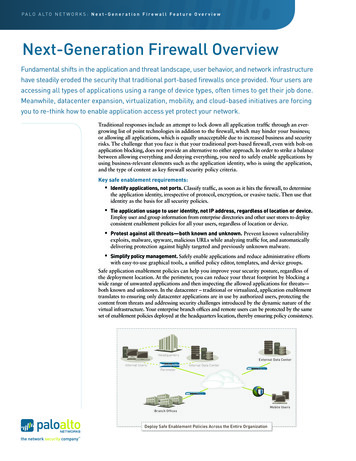
Transcription
Next generation Advanced Packaging usinginnovative laser assisted assembly processesNew key technologies in advanced packaging and interconnection technology like µLEDs, heterogenousintegration, cubing, ultra-thin flex, embedded packaging, optical packaging etc. dominate not only thecontents of podium discussions at conferences and exhibitions, they also impact the growth projectionsand analyses of technical rating agencies.The goal of many companies concerned with chip size packaging (CSP) is to develop and offer processsolutions fitting the highly complex demands of these new technologies for an efficient bondingtechnology.As a world leader in wafer bumping & advanced packaging including an own machine production,PacTech, since 1995, deals with the development of innovative laser enabled process technologies aswell as the provision of the respective machine system solutions.The main problem in conventional bonding techniques, like the thermo compression bonding (TCB), thethermosonic wire bonding (TS) or the bonding via an oven reflow, lies in the introduction of high thermalloads and in the case of the TCB and TS-Bonding mechanical loads during the bonding process.Common to all of them is the risk for creating mechanical stresses in the bonds as well as the wholepackage, which can be primarily identified via global and local warpage, positional offsets of the bondingpads, micro cracks in the intermetallic compound layers and delamination effects of the redistributionlayer (RDL), as well as bonding fails at the contacts and the contact interfaces to the substrate.These lead to performance losses, reduced usability and reduced life cycle times of the finished product.Machine producers undertake great efforts to solve or compensate for this problem via proceduralmeans. For example, many conventional bonders are equipped with heated substrate holders or heatedprocess gases, which on the one hand are to minimize the temperature difference when joining thecomponents and on the other hand should reduce the thermal load using heated active process gases.These approaches, however, reach their limits when it comes to new material combinations and theongoing miniaturization. Especially the bonding of ultra-thin organic and inorganic materials paired withsimultaneous reduction of the contact pad geometries down to few µm or the bonding of pure metalpads such as Cu on Cu are problematic.All of the above justifies the call for a thermally and mechanically minimally interactive principle for thebonding process.As the leading capacity in the area of laser enabled bonding of solder spheres and semiconductorelements, PacTech holds the key to a localized, low stress and selective bonding process by introducingthe necessary energy optically via a laser.The main advantage, apart from interaction times of less than 1s, is that the optical energy can becoupled right into the bonding position by taking the absorption coefficients of the respective elementsinto account and choosing the optimal wavelength.This way, thermal loads can be omitted, mechanical stresses avoided and diffusion effects at theinterfaces reduced to a minimum, which is paramount in very small bonding pads of less than 1µm asfound in opto-electronic packages.Figure A1 shows a characteristic laser reflow profile, while figure A2 shows the respective modulatedpower density distribution of the laser beam for a force free bonding of a 1.1mm x 1.1mm x 150µm bluelight InGaN LED with a 3µm Sn20Au80 solder layer onto a Ag plated Cu lead frame. The bonding takesplace within a timeframe of 250ms.
Fig. A1: Laser reflow profile for an LED assemblyFig. A2: Laser power distribution for an LED assembly.This compares to a conventional TCB process, which takes place in a time frame of 8s at 280 C andunder a force corresponding to the weight of 1kg.The carrier substrate is also pre-heated to above 200 C to reduce the losses due to thermal conduction.The thermal energy is not introduced directly at the bonding interface but conducted through the elementto be bonded, which is practically repurposed as a thermode.The described process parameters and procedures demonstrate the advantages of the optical insertionof energy compared to the conventional thermal conduction through the whole element.Additionally, a much more beneficial IMC formation can be observed (Figure A3). Studies show, thatthis laser reflow characteristic IMC has higher life cycle times because it experiences lower phasegrowth.Fig. A3: IMC structure of a 40µm Cu-Pillar LAB bondThese advantages of the thermal and dynamic interaction during the bonding of the laser assistedbonding (LAB) process, paired with the increased life cycle time, find a broad range of applications inPacTech’s process portfolio.Several of the newer applications will be presented in the following sections:LAPLACE LAdB Laser Assisted de-BondingBy reversing the process sequence of our established laser enabled bonding process for microchips(LAPLACE LAB), innovative solutions for removing faulty elements and packages (like SoP, SiP, PoPetc.) could be developed.The process principle of laser enabled removal (LAPLACE LAdB) of faulty semiconductor elements andpackages is sketched in Figure B1.
Fig. B1: Process principle of laser enabled removal of faulty elementsTo perform the process, one starts by placing the bond tool onto the faulty semiconductor element(daughter substrate) and applying a vacuum inside the tool.Next, the laser, which is adapted to the package to be processed in its wavelength and power densitydistribution, is activated and shot at the bonding interface.Within just a few ms, the solder liquefies and is separated via a vertical axis movement of the bond tool.The instantaneous supply of nitrogen prevents any oxidation during the liquid phase.The advantages compared to conventional repair solutions, which are based on mechanically abrasiveprocesses like grinding and polishing or thermode processes introducing massive thermal loads, areobvious because the minimally invasive introduction of heat energy damages neither neighboringfunctional chip layers nor passivation or metallization layers.Our investigations show, that using flux or special process gases, the residual solder assumes a quality,which allows for the direct bonding of a new chip (Figure B2).Fig. B2: Removal of a faulty PoP via LAPLACE LAdBUsing PacTech’s technology even chips with a Cu-Pillar interface can be repaired up to four times beforea deviation in quality, reliability and life cycle is to be expected.Figure B3 shows the residual solder on the flex board of a chip on board application with 40µm Cu pillarbonds.Fig. B3: Residual solder on a 40µm contact pad
This also requires a sufficient precision of the bond system. PacTech offers, among other systems, themulti-functional bond platform LAPLACE “Genesis”, which reaches positioning accuracies in the subµm regime using a combination of highly precise axis systems, a unique recognition mechanism and anano positioning system (Figure B4).Fig. B4: LAPLACE-GENESIS bond platformSB²-WB Laser Soldered Wire BondingAll conventional wire bond processes like thermosonic (TS), ultrasonic (US) or thermo compression (TC)bonding have the introduction of strong mechanical forces (30-90cN) or large thermal loads (100 C250 C) at the bonding interface in common.Applications on brittle materials such as GaAs, PZT-ceramics, organic thin films ( 20µm) like an MCMD-type package or vibration sensitive pins cannot be equipped with a conventional wire bond in a reliableand reproducible manner.Additionally, the material structure of the wire is being transformed during the electric flame off (EFO) orthe ultrasonic welding.A characteristic property of this is the so called “neck-break” failure mode on wire pull tests.To overcome this problem, PacTech developed the SB²-WB wire bond process. At the core of thisinnovative solution for the creation of alternative low stress wire bonds on the chip level or substratelevel sits a combination of the unique SB²-Jet solder jetting principle with a wire feeding unit.The simplified working principle is illustrated in Figure C1.Fig. C1: Principle of the SB²-WB process
The wire is fed onto the contact pad underneath the solder jet capillary. Almost simultaneously to thefeeding and positioning of the wire, a molten solder sphere is applied to the wire. Compared to competingprocesses, this process can be regarded as mechanically contactless as the force created by the solderlies in the µN regime.The bonding process itself happens within a time regime of less than 10ms as it is performed usinglaser. Next, the wire is pulled over to the corresponding contact, forming a loop if needed, and bondedusing a solder ball analogous to the first contact. Finally, the wire is cut using a blade, pulling force orwell-proportioned laser pulse. Alternatively, to the conventional processes, the wire can be continued tofurther contact pads and bonded to them without intermission or change to the wire profile.An example for an application is shown in Figure C2, the wire bond is realized between vibrationallysensitive pins and a LTTC carrier substrate.Fig. C2: SB²-WB wire bonds in a plug moduleFigure C3, shows a lateral SB²-WB wire bond on a sensor housing.Fig. C3: SB²-WB wire bond on a sensor housingThe SB²-WB process allows for the formation of the typical loop forms in the bond wire. Anotheradvantage is, that the SB²-WB process can be geometrically tailored such that the wire exits the solderbond in a direct lateral fashion without any vertical component. Thus, the height of this variant is lowerthan that of ultra-low loop (ULL) or stand-off stitch bond (SSB) solutions in conventional wire bondingprocesses.Our studies show that the expected stability and life cycle durations match or even exceed those ofconventional wire bonding techniques for soft solders and in dependence of the chosen wire diameterand solder sphere volume.For example, performing a current load capability test a more advantageous heat distribution could beidentified (Figure C4).
Fig. C4: Optical temperature measurement under current load (FHG-ENAS)The above result is mainly caused by the advantageous property of the SB²-WB process of not changingthe material structure of the wire through thermo mechanical effects.Another advantage lies in the simple repairability of faulty contacts, as these can easily be de- andrebonded.Because of the intermetallic compounds, which are characteristic for the short laser reflow, this processcan be repeated several times without a loss in performance arising.The newly developed SB²-WB process can process and bond wires in the range of 15µm-500µm. Thesmallest processable pitch lies around 40µm. All common solderable wire materials can be processedreliably with a speed of up to 6 bonds per second.SB²-Jet Macro Solder Ball BumpingThe classic area of placement technology of wired elements via through hole technology (THT) alsocalls for alternative solutions to overcome the technical disadvantages of wave, selective and handsoldering for future generations of circuit boards for certain applications.PacTech focuses on the omission of flux and the resulting reduction of subsequent cleaning steps aswell as the bonding of smaller wire distances resulting in higher package densities and the soldering ofhardly accessible contacts.This is why PacTech has broadened its spectrum of processable solder ball sizes of 30µm-760µm andnow offers support for sizes of up to 2000µm to serve the volume needs of the through hole technologyassembly.The overall process principle of the SB²-Jet process stays the same even with these very large solderballs (Figure D1).Fig. D1: Principle of the SB²-Jet processThe solder spheres are singulated in a specialized bond head and enter a capillary. The diameter of thecapillary’s lower opening is smaller than that of the solder ball, which forces the ball to a halt at the tipof the capillary.
Via a laser pulse, the solder ball is molten and applied to the bond contact by nitrogen pressure. Uponarrival on the contact pad, the solder assumes a spherical shape (solder bump) again, due to its surfacetension.The advantageous process characteristic is conserved unconditionally even in very large solder ballsizes. The local, selective and flux free bonding from a distance of up to five times the solder balldiameter provides manufacturers of circuit board based products with new perspectives.For example, the bonding can take place deep inside a casing or at a moment in time, when furthercleaning steps are already prohibited.Figure D2 shows an example for an application on a LTCC carrier for a head light module.Fig. D2: THT contact pin soldering in the casing of a head light moduleFig. D3: THT plug casing contacting through circuit boardAgain, PacTech offers a broad spectrum of machine solutions. Figure D4 shows an exemplary availablemachine platform.Fig. D4: SB²-Jet dual bonder
Inside the system either several universal 3D axis systems or PacTech’s robotic solution with a bondhead effector can be integrated. The system contains a loading, transfer and unloading unit to allow fora fully automated operation. Universal interfaces for data communication, RFID or code reader come aspart of the standard.In conclusion, PacTech’s state-of-the-art laser-assisted bonding/de-bonding technologies offercompelling benefits in the form of low optical interaction times ( 1s), topical/local interaction with ultrahigh precision (μm), high-quality IMCs, and ultra-low thermal and mechanical stresses (μN). A widerange of solder sphere (wire) sizes and compositions could be used. In addition to robust processes andspecialized machine systems outlined above for solder- and wire-bonding applications, PacTech offersa multitude of other innovative and alternate solutions (e.g. cantilever, capacitor, LED) tailored for eachrespective application to fulfill complex demands while simultaneously offering high productivity andyield. PacTech strives to be at the forefront of offering agile solutions for sophisticated problems inrelation to applications involving flip-chips, probe cards, MOSFETs, diodes, μLEDs, RF, etc. Our goal isto actively shape the bonding technologies of tomorrow and beyond.About PacTechPac Tech – Packaging Technologies GmbH is a world leading provider of advanced wafer bumping,packaging and solder ball placement equipment. As an innovator in the area of Laser Assisted SolderJetting and Laser Chip Bonding, PacTech provides high accuracy high speed high flexibility solderbonding solutions for semiconductors and additional electronic components, alongside with its uniqueturnkey solution for wafer level electroless plating including process, equipment and chemical suppliesfrom a single source.For more than 25 years and with great success, PacTech supports besides equipment manufacturing,subcontracting services for high volume production and engineering projects on wafer, substrate andchip level at the sites in Germany, the U.S. & Malaysia with by now nearly 400 employees.From electroless Ni/Au or Ni/Pd Under Bump Metallization (UBM) for Flip Chip or WLCSP, electrolessNi/Pd/Au OPM for Au or Cu wire bonding, electroplated Cu Pillars, solder balling via Single Jetting (SB²),Ball Drop Stencil Technology (Ultra-SB²) and wire soldering to a multitude of back-end services,PacTech provides a broad range of highly specialized technology solutions.For more information, contact:Thomas OppertPacTech – Packaging Technologies GmbHAm Schlangenhorst 7-9D-14641 Nauen, Germanytel: 49 (0) 3321 4495 100email: sales@pactech.de
Next generation Advanced Packaging using innovative laser assisted assembly processes New key technologies in advanced packaging and interconnection technology like µLEDs, heterogenous integration, cubing, ultra-thin flex, embedded packaging, optical packaging etc. dominate not only the . multi-funct