Transcription
PRELIMINARY80296SA COMMERCIALCHMOS 16-BIT MICROCONTROLLER 50 MHz Operation† Chip-select Unit— 6 Chip-select Pins 6 Mbytes of Linear Address Space— Dynamic Demultiplexed/MultiplexedAddress/Data Bus for EachChip Select 512 Bytes of Register RAM 2 Kbytes of Code/Data RAM Register-register Architecture Footprint and Functionally CompatibleUpgrade for the 8XC196NP and80C196NU Optional Phase-locked Loop (PLL)Circuitry with 2x or 4x Clock Multiplier 32 I/O Port Pins 19 Interrupt Sources, 14 withProgrammable Priorities 4 External Interrupt Pins and NMI Pin 2 Flexible 16-bit Timer/Counters withQuadrature Counting Capability— Programmable Wait States(0–15) for Each Chip Select— Programmable Bus Width(8- or 16-bit) for Each Chip Select— Programmable Address Range forEach Chip Select Event Processor Array (EPA) with4 High-speed Capture/CompareChannels Multiply and Accumulate Executes in80 ns Using the 40-bit HardwareAccumulator 3 Pulse-width Modulator (PWM)Outputs with High Drive Capability 880 ns 32/16 Unsigned Division Full-duplex Serial Port with DedicatedBaud-rate Generator Complete System DevelopmentSupport†40 MHz standard; 50 MHz is Speed Premium 100-pin QFP Package High-speed CHMOS TechnologyThe 80296SA is a member of Intel’s 16-bit MCS 96 microcontroller family. The 80296SA features 6 Mbytesof linear address space, a demultiplexed bus, and a chip-select unit. The external bus can dynamically switchbetween multiplexed and demultiplexed operation. The device has hardware and instructions to supportvarious digital signal processing algorithms.NOTEThis datasheet contains information on new products in production. The specificationsare subject to change without notice. Verify with your local Intel sales office that you havethe latest datasheet before finalizing a design.COPYRIGHT INTEL CORPORATION, 1997January 1997Order Number: 272748-003
Information in this document is provided in connection with Intel products. No license, express or implied, byestoppel or otherwise, to any intellectual property rights is granted by this document. Except as provided inIntel’s Terms and Conditions of Sale for such products, Intel assumes no liability whatsoever, and Intel disclaims any express or implied warranty, relating to sale and/or use of Intel products including liability or warranties relating to fitness for a particular purpose, merchantability, or infringement of any patent, copyright orother intellectual property right. Intel products are not intended for use in medical, life saving, or life sustainingapplications.Intel retains the right to make changes to specifications and product descriptions at any time, without notice.*Third-party brands and names are the property of their respective owners.Copies of documents which have an ordering number and are referenced in this document, or other Intel literature, may be obtained from:Intel CorporationP.O. Box 7641Mt. Prospect, IL 60056-7641or call 1-800-548-4725
CONTENTS80296SA CommercialCHMOS 16-bit Microcontroller1.0 Product Overview . 12.0 Nomenclature Overview. 23.0 Pinout . 34.0 Signals . 65.0 Address Map . 136.0 Electrical Characteristics . 146.1 DC Characteristics. 146.2 AC Characteristics. 186.2.1 Relationship of XTAL1 to CLKOUT . 186.2.2 Explanation of AC Symbols . 196.2.3 AC Characteristics — Multiplexed Bus Mode . 206.2.3.1 System Bus Timings, Multiplexed Bus . 226.2.3.2 READY Timing, Multiplexed Bus . 236.2.4 AC Characteristics — Demultiplexed Bus Mode . 246.2.4.1 System Bus Timings, Demultiplexed Bus . 266.2.4.2 READY Timing, Demultiplexed Bus . 276.2.4.3 80296SA Deferred Bus Timing Mode . 286.2.5 HOLD#, HLDA# Timings . 296.2.6 AC Characteristics — Serial Port, Synchronous Mode 0 . 306.2.7 External Clock Drive . 317.0 Thermal Characteristics . 338.0 80296SA Errata. 339.0 Datasheet Revision History . SA Block Diagram .1The 80296SA Family Nomenclature .280296SA 100-pin QFP Package .3ICC versus Frequency in Reset . 17Effect of Clock Mode on CLKOUT. 18System Bus Timings, Multiplexed Bus Mode . 22Example READY Timings at 50 MHz, Multiplexed Bus, BUSCONx 1 Wait State. 23System Bus Timings, Demultiplexed Bus Mode. 26Example READY Timings at 50 MHz, Demultiplexed Bus, BUSCONx 1 Wait State . 27Deferred Bus Mode Timing Diagram. 28HOLD#, HLDA# Timing Diagram . 29Serial Port Waveform — Synchronous Mode 0. 30External Clock Drive Waveforms. 31AC Testing Input and Output Waveforms During 5.0 Volt Testing . 32Float Waveforms During 5.0 Volt Testing. 32PRELIMINARYiii
ivDescription of Product Nomenclature . 280296SA 100-pin QFP Pin Assignment . 480296SA 100-pin QFP Pin Assignment Arranged by Functional Categories . 5Signal Descriptions . 680296SA Address Map . 13DC Characteristics Over Specified Operating Conditions. 14AC Timing Symbol Definitions. 19AC Characteristics the 80C296SA Will Meet, Multiplexed Bus Mode . 20AC Characteristics the External Memory System Must Meet, Multiplexed Bus Mode . 21AC Characteristics the 80C296SA Will Meet, Demultiplexed Bus Mode . 24AC Characteristics the External Memory System Must Meet, Demultiplexed Bus Mode . 25HOLD#, HLDA# Timings . 29Serial Port Timing — Synchronous Mode 0 . 30External Clock Drive. 31Thermal Characteristics . 33PRELIMINARY
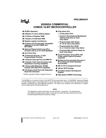
80296SA COMMERCIAL CHMOS 16-BIT MICROCONTROLLER1.0PRODUCT OVERVIEWThe 80296SA is a member of Intel’s 16-bit MCS 96 microcontroller family. The 80296SA features 6 Mbytesof linear address space, a demultiplexed bus, and a chip-select unit. The external bus can dynamically switchbetween multiplexed and demultiplexed operation. The device has hardware and instructions to supportvarious digital signal processing algorithms.Code/DataRAM(2 Kbytes)Port 3Memory Addr Bus (24)SIOMemory Data Bus (16)Chip-selectUnitBus Control SignalsA19:16BaudrateGeneratorPort AlignerQueuePort 4InstructionSequencerRegister File(3-port RAM)MemoryInterfaceUnitDestination Addr (24)Destination Data (16)Peripheral Addr Bus (8)ALUEPAPeripheral Data Bus (16)Source 2 Addr (24)Source 2 Data (16)Memory Addr Bus (24)Source 1 Addr (24)Source 1 Data (16)Memory Data Bus (16)InterruptControllerTimer 1Timer 2Port 1A3175-02Figure 1. 80296SA Block DiagramPRELIMINARY1
80296SA COMMERCIAL CHMOS 16-BIT MICROCONTROLLER2.0NOMENCLATURE OVERVIEWXXX8XXXXXXXXXagi aTeA2815-01Figure 2. The 80296SA Family NomenclatureTable 1. Description of Product NomenclatureParameterTemperature and Burn-in OptionsDescriptionno markCommercial operating temperature range (0 C to 70 C)with Intel standard burn-in.Packaging OptionsSQFPProgram–memory Options0Without ROMProcess InformationProduct FamilyDevice Speed2Optionsno mark296SACHMOS—4040 MHz5050 MHzPRELIMINARY
80296SA COMMERCIAL CHMOS 16-BIT D11AD12AD13AD14AD15A16 / EPORT.0A17 / 24252627282930S80296SAView of component asmounted on PC 857565554535251VSSA18 / EPORT.2A19 / EPORT.3WR# / WRL#RD#BHE# / 3A14A15VSSXTAL1XTAL2VSSP2.7 / CLKOUTVCCP2.6 / HLDA#P2.5 / HOLD#P1.1 / EPA1P1.2 / EPA2P1.3 / EPA3P1.4 / T1CLKP1.5 / T1DIRVCCP1.6 / T2CLKVSSP1.7 / T2DIRP4.0 / PWM0P4.1 / PWM1P4.2 / PWM2P4.3VCCVSSP2.0 / TXDP2.1 / RXDP2.2 / EXTINT0P2.3 / BREQ#P2.4 / 0 / CS0#P3.1 / CS1#P3.2 / CS2#P3.3 / CS3#VSSP3.4 / CS4#P3.5 / CS5#P3.6 / EXTINT2NCP3.7 / EXTINT3P1.0 / EPA0VCCA3155-02Figure 3. 80296SA 100-pin QFP PackagePRELIMINARY3
80296SA COMMERCIAL CHMOS 16-BIT MICROCONTROLLERTable 2. 80296SA 100-pin QFP Pin 3.651HOLD#/P2.576RD#2NC (see Note)27NC (see T.2/A185NC (see P3.550EXTINT1/P2.475BHE#/WRH#100AD1NOTE:4PinFor compatibility with future products, tie pin 5 to VCC and leave pins 2 and 27 unconnected.PRELIMINARY
80296SA COMMERCIAL CHMOS 16-BIT MICROCONTROLLERTable 3. 80296SA 100-pin QFP Pin Assignment Arranged by Functional CategoriesAddress & Data(continued)Address & DataNameNamePower & .1A210AD1485CS2#/P3.2A311AD1584CS3#/P3.3A412Bus Control & C8132VCC93Processor MINARYNameNo ConnectionNamePin25
80296SA COMMERCIAL CHMOS 16-BIT MICROCONTROLLER4.0SIGNALSTable 4. Signal DescriptionsNameA15:0TypeI/ODescriptionSystem Address BusThese address pins provide address bits 0–15 during the entire external memorycycle during both multiplexed and demultiplexed bus modes.A19:16I/OAddress Pins 16–19These address pins provide address bits 16–19 during the entire external memorycycle during both multiplexed and demultiplexed bus modes, supporting extendedaddressing of the 1-Mbyte address space.NOTE: Internally, there are 24 address bits; however, only 20 external addresspins (A19:0) are implemented. The internal address space is 16 Mbytes(000000–FFFFFFH) and the external address space is 1 Mbyte (00000–FFFFFH). The microcontroller resets to FF2080H.A19:16 share package pins with EPORT.3:0.AD15:0I/OAddress/Data LinesThese pins provide a multiplexed address and data bus. During the address phaseof the bus cycle, address bits 0–15 are presented on the bus and can be latchedusing ALE or ADV#. During the data phase, 8- or 16-bit data is transferred.AD7:0 share package pins with P3.7:0. AD15:8 share package pins with P4.7:0.ALEOAddress Latch EnableThis active-high output signal is asserted only during external memory cycles. ALEsignals the start of an external bus cycle and indicates that valid address informationis available on the system address/data bus (A19:16 and AD15:0 for a multiplexedbus; A19:0 for a demultiplexed bus).An external latch can use this signal to demultiplex address bits 0–15 from theaddress/data bus in multiplexed mode.BHE#OByte High Enable†During 16-bit bus cycles, this active-low output signal is asserted for word and highbyte reads and writes to external memory. BHE# indicates that valid data is beingtransferred over the upper half of the system data bus. Use BHE#, in conjunctionwith address bit 0 (A0 for a demultiplexed address bus, AD0 for a multiplexedaddress/data bus), to determine which memory byte is being transferred over thesystem bus:BHE#AD0 or A0 Byte(s) Accessed001010both byteshigh byte onlylow byte onlyBHE# shares a package pin with WRH#.†6Chip configuration register 0 (CCR0) determines whether this pin functions asBHE# or as WRH#. CCR0.2 1 selects BHE#; CCR0.2 0 selects WRH#.PRELIMINARY
80296SA COMMERCIAL CHMOS 16-BIT MICROCONTROLLERTable 4. Signal Descriptions (Continued)NameBREQ#TypeODescriptionBus RequestThis active-low output signal is asserted during a hold cycle when the bus controllerhas a pending external memory cycle. When the bus-hold protocol is enabled(WSR.7 is set), the P2.3/BREQ# pin can function only as BREQ#, regardless of theconfiguration selected through the port configuration registers (P2 MODE, P2 DIR,and P2 REG). An attempt to change the pin configuration is ignored until the bushold protocol is disabled (WSR.7 is cleared).The microcontroller can assert BREQ# at the same time as or after it assertsHLDA#. Once it is asserted, BREQ# remains asserted until HOLD# is deasserted.BREQ# shares a package pin with P2.3.CLKOUTOClock OutputOutput of the internal clock generator. The CLKOUT frequency is ½ the internaloperating frequency (f). CLKOUT has a 50% duty cycle.CLKOUT shares a package pin with P2.7.CS5:0#OChip-select Lines 0–5The active-low output CSx# is asserted during an external memory cycle when theaddress to be accessed is in the range programmed for chip select x or chip selectx 1 if remapping is enabled. If the external memory address is outside the rangeassigned to the six chip selects, no chip-select output is asserted and the busconfiguration defaults to the CS5# values.Immediately following reset, CS0# is automatically assigned to the range FF2000–FF20FFH.CS5:0# share package pins with P3.5:0.EPA3:0I/OEvent Processor Array (EPA) Capture/Compare ChannelsHigh-speed input/output signals for the EPA capture/compare channels. For highspeed PWM applications, the outputs of two EPA channels (either EPA0 and EPA1or EPA2 and EPA3) can be remapped to produce a PWM waveform on a sharedoutput pin.EPA3:0 share package pins with P1.3:0.EPORT.3:0I/OExtended Addressing PortThis is a standard 4-bit, bidirectional port.EPORT.3:0 share package pins with A19:16.PRELIMINARY7
80296SA COMMERCIAL CHMOS 16-BIT MICROCONTROLLERTable 4. Signal Descriptions (Continued)NameTypeEXTINT3:0IDescriptionExternal InterruptsThese programmable interrupts are controlled by the EXTINT CON register. Thisregister controls whether the interrupt is edge-triggered or level-sensitive andwhether a rising edge/high level or falling edge/low level activates the interrupt.In standby and powerdown modes, asserting the EXTINTx signal causes the deviceto resume normal operation. The interrupt does not need to be enabled, but the pinmust be configured as a special-function input. If the EXTINTx interrupt is enabled,the CPU executes the interrupt service routine. Otherwise, the CPU executes theinstruction that immediately follows the command that invoked the power-savingmode.In idle mode, asserting any enabled interrupt causes the device to resume normaloperation.EXTINT0 shares a package pin with P2.2, EXTINT1 shares a package pin withP2.4, EXTINT2 shares a package pin with P3.6, and EXTINT3 shares a package pinwith P3.7.HLDA#OBus Hold AcknowledgeThis active-low output indicates that the CPU has released the bus as the result ofan external device asserting HOLD#. When the bus-hold protocol is enabled(WSR.7 is set), the P2.6/HLDA# pin can function only as HLDA#, regardless of theconfiguration selected through the port configuration registers (P2 MODE, P2 DIR,and P2 REG). An attempt to change the pin configuration is ignored until the bushold protocol is disabled (WSR.7 is cleared).HLDA# shares a package pin with P2.6.HOLD#IBus Hold RequestAn external device uses this active-low input signal to request control of the bus.When the bus-hold protocol is enabled (WSR.7 is set), the P2.5/HOLD# pin canfunction only as HOLD#, regardless of the configuration selected through the portconfiguration registers (P2 MODE, P2 DIR, and P2 REG). An attempt to changethe pin configuration is ignored until the bus-hold protocol is disabled (WSR.7 iscleared).HOLD# shares a package pin with P2.5.INSTOInstruction FetchWhen high, INST indicates that an instruction is being fetched from externalmemory. The signal remains high during the entire bus cycle of an externalinstruction fetch. INST is low for data accesses, including interrupt vector fetchesand chip configuration byte reads. INST is low during internal memory fetches.8PRELIMINARY
80296SA COMMERCIAL CHMOS 16-BIT MICROCONTROLLERTable 4. Signal Descriptions (Continued)NameNMITypeIDescriptionNonmaskable InterruptIn normal operating mode, a rising edge on NMI generates a nonmaskable interrupt.NMI has the highest priority of all interrupts except trap and unimplemented opcode.Assert NMI for greater than one state time to guarantee that it is recognized.If NMI is held high during and immediately following reset, the microcontroller willexecute the NMI interrupt service routine when code execution begins. To preventan inadvertent NMI interrupt vector, the first instruction (at F2080H) must clear theNMI pending interrupt bit.ANDB INT PEND1, #7FH.During idle mode, a rising edge on NMI causes the microcontroller to exit idle modeand branch to the interrupt service routine.ONCEIOn-circuit EmulationHolding ONCE high during the rising edge of RESET# places the microcontrollerinto on-circuit emulation (ONCE) mode. This mode puts all pins, except READY,RESET#, ONCE, and NMI, into a high-impedance state, thereby isolating themicrocontroller from other components in the system. The value of ONCE is latchedwhen the RESET# pin goes inactive. While the microcontroller is in ONCE mode,you can debug the system using a clip-on emulator.To exit ONCE mode, reset the microcontroller by pulling the RESET# signal low. Toprevent inadvertent entry into ONCE mode, connect the ONCE pin to VSS.P1.7:0I/OPort 1This is a standard, 8-bit, bidirectional port that shares package pins with individuallyselectable special-function signals.Port 1 shares package pins with the following signals: P1.0/EPA0, P1.1/EPA1,P1.2/EPA2, P1.3/EPA3, P1.4/T1CLK, P1.5/T1DIR, P1.6/T2CLK, and P1.7/T2DIR.P2.7:0I/OPort 2This is a standard, 8-bit, bidirectional port that shares package pins with individuallyselectable special-function signals.Port 2 shares package pins with the following signals: P2.0/TXD, P2.1/RXD,P2.2/EXTINT0, P2.3/BREQ#, P2.4/EXTINT1, P2.5/HOLD#, P2.6/HLDA#, andP2.7/CLKOUT.P3.7:0I/OPort 3This is a standard, 8-bit, bidirectional port that shares package pins with individuallyselectable special-function signals.Port 3 shares package pins with the following signals: P3.0/CS0#, P3.1/CS1#,P3.2/CS2#, P3.3/CS3#, P3.4/CS4#, P3.5/CS5#, P3.6/EXTINT2, andP3.7/EXTINT3.P4.3:0I/OPort 4Port 4 is a standard, 4-bit, bidirectional I/O port with high-current drive capability.Port 4 shares package pins with the following signals: P4.0/PWM0, P4.1/PWM1,and P4.2/PWM2. P4.3 has a dedicated package pin.PRELIMINARY9
80296SA COMMERCIAL CHMOS 16-BIT MICROCONTROLLERTable 4. Signal Descriptions d Loop 1 and 2 EnableThese input pins enable the on-chip clock multiplier feature and select either thedoubled or the quadrupled clock speed:PLLEN20011PLLEN10101Mode1x mode; PLL disabled; f FXTAL12x mode; PLL enabled; f 2FXTAL1Reserved †4x mode; PLL enabled; f 4FXTAL1†CAUTION: This reserved combination causes the device to enter an unsupportedtest mode.PWM2:0OPulse Width Modulator OutputsThese are PWM output pins with high-current drive capability. The duty cycle andfrequency-pulse-widths are programmable.PWM2:0 share package pins with P4.2:0.RD#OReadRead-signal output to external memory. RD# is asserted during external memoryreads.READYIReady InputThis active-high input can be used to insert wait states in addition to thoseprogrammed in chip configuration byte 0 (CCB0) and the bus control x register(BUSCONx).CCB0 is programmed with the minimum number of wait states (0, 5, 10, 15) for anexternal fetch of CCB1, and BUSCONx is programmed with the minimum number ofwait states (0–15) for all external accesses to the address range assigned to thechip-select x channel.If the programmed number of wait states is greater than zero and READY is lowwhen this programmed number of wait states is reached, additional wait states areadded until READY is pulled high. If the programmed number of wait states is equalto zero, hold the READY pin high. Programming the number of wait states equal tozero and holding the READY pin low produces unpredictable results.RESET#I/OResetA level-sensitive reset input to, and an open-drain system reset output from, themicrocontroller. Either a falling edge on RESET# or an internal reset turns on a pulldown transistor connected to the RESET# pin for 16 state times.In the powerdown, standby, and idle modes, asserting RESET# causes themicrocontroller to reset and return to normal operating mode. If the phase-lockedloop (PLL) clock circuitry is enabled, you must hold RESET# low for at least 2 ms toallow the PLL to stabilize before the internal CPU and peripheral clocks are enabled.After a reset, the first instruction fetch is from FF2080H.10PRELIMINARY
80296SA COMMERCIAL CHMOS 16-BIT MICROCONTROLLERTable 4. Signal Descriptions (Continued)NameRPDTypeIDescriptionReturn from PowerdownTiming pin for the return-from-powerdown circuit.If your application uses powerdown mode, connect a capacitor between RPD andVSS if either of the following conditions are true. the internal oscillator is the clock source the phase-locked loop (PLL) circuitry is enabled (see PLLEN2:1 signaldescription)The capacitor causes a delay (at least 2 ms) that enables the oscillator and PLLcircuitry to stabilize before the internal CPU and peripheral clocks are enabled.Refer to the “Special Operating Modes” chapter of the 80296SA MicrocontrollerUser’s Manual for details on selecting the capacitor.The capacitor is not required if your application uses powerdown mode and if bothof the following conditions are true. an external clock input is the clock source the phase-locked loop circuitry is disabledIf your application does not use powerdown mode, leave this pin unconnected.RXDI/OReceive Serial DataIn modes 1, 2, and 3, RXD receives serial port input data. In mode 0, it functions aseither an input or an open-drain output for data.RXD shares a package pin with P2.1.T1CLKITimer 1 External ClockExternal clock for timer 1. Timer 1 increments (or decrements) on both rising andfalling edges of T1CLK. Also used in conjunction with T1DIR for quadraturecounting mode.andExternal clock for the serial I/O baud-rate generator input (program selectable).T1CLK shares a package pin with P1.4.T2CLKITimer 2 External ClockExternal clock for timer 2. Timer 2 increments (or decrements) on both rising andfalling edges of T2CLK. It is also used in conjunction with T2DIR for quadraturecounting mode.T2CLK shares a package pin with P1.6.T1DIRITimer 1 External DirectionExternal direction (up/down) for timer 1. Timer 1 increments when T1DIR is high anddecrements when it is low. Also used in conjunction with T1CLK for quadraturecounting mode.T1DIR shares a package pin with P1.5.T2DIRITimer 2 External DirectionExternal direction (up/down) for timer 2. Timer 2 increments when T2DIR is high anddecrements when it is low. It is also used in conjunction with T2CLK for quadraturecounting mode.T2DIR shares a package pin with P1.7.PRELIMINARY11
80296SA COMMERCIAL CHMOS 16-BIT MICROCONTROLLERTable 4. Signal Descriptions (Continued)NameTXDTypeODescriptionTransmit Serial DataIn serial I/O modes 1, 2, and 3, TXD transmits serial port output data. In mode 0, it isthe serial clock output.TXD shares a package pin with P2.0.VCCPWRDigital Supply VoltageConnect each VCC pin to the digital supply voltage.VSSGNDDigital Circuit GroundThese pins supply ground for the digital circuitry. Connect each VSS pin to groundthrough the lowest possible impedance path.WR#OWrite†This active-low output indicates that an external write is occurring. This signal isasserted only during external memory writes.WR# shares a package pin with WRL#.†WRH#OChip configuration register 0 (CCR0) determines whether this pin functions asWR# or WRL#. CCR0.2 1 selects WR#; CCR0.2 0 selects WRL#.Write High†During 16-bit bus cycles, this active-low output signal is asserted for high-byte writesand word writes to external memory. During 8-bit bus cycles, WRH# is asserted forall write operations.WRH# shares a package pin with BHE#.†WRL#OChip configuration registrer 0 (CCR0) determines whether this pin functions asBHE# or WRH#. CCR0.2 1 selects BHE#; CCR0.2 0 selects WRH#.Write Low†During 16-bit bus cycles, this active-low output signal is asserted for low-byte writesand word writes to external memory. During 8-bit bus cycles, WRL# is asserted forall write operations.WRL# shares a package pin with WR#.†XTAL1IChip configuration register 0 (CCR0) determines whether this pin functions asWR# or WRL#. CCR0.2 1 selects WR#; CCR0.2 0 selects WRL#.Input Crystal/Resonator or External Clock InputInput to the on-chip oscillator, internal phase-locked loop circuitry, and the internalclock generators. The internal clock generators provide the peripheral clocks, CPUclock, and CLKOUT signal. When using an external clock source instead of the onchip oscillator, connect the clock input to XTAL1. The external clock signal mustmeet the VIH specification for XTAL1.XTAL2OInverted Output for the Crystal/ResonatorOutput of the on-chip oscillator inverter. Leave XTAL2 floating when the design usesan external clock source instead of the on-chip oscillator.12PRELIMINARY
80296SA COMMERCIAL CHMOS 16-BIT MICROCONTROLLER5.0ADDRESS MAPTable 5. 80296SA Address MapHexAddressDescription (Note 1, Note 2)Addressing Modes forData AccessesFFFFFFFFF800External device (memory or I/O) in 1-Mbyte mode (CCB1.1 0)A copy of internal code RAM in 64-Kbyte mode (CCB1.1 1)ExtendedFFF7FFFF2080External program memory (Note 3)ExtendedFF207FFF
80296SA COMMERCIAL CHMOS 16-BIT MICROCONTROLLER 1.0 PRODUCT OVERVIEW The 80296SA is a member of Intel's 16-bit MCS 96 microcontroller family. The 80296SA features 6 Mbytes of linear address space, a demultiplexed bus, and a chip-select unit. The external bus can dynamically switch