Transcription
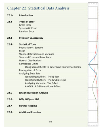
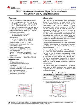
TMP117SNOSD82D – JUNE 2018 – REVISED SEPTEMBER 2022TMP117 High-Accuracy, Low-Power, Digital Temperature SensorWith SMBus - and I2C-Compatible Interface1 Features3 Description The TMP117 is a high-precision digital temperaturesensor. It is designed to meet ASTM E1112and ISO 80601 requirements for electronic patientthermometers. The TMP117 provides a 16-bittemperature result with a resolution of 0.0078 Cand an accuracy of up to 0.1 C across thetemperature range of –20 C to 50 C with nocalibration. The TMP117 has in interface that isI2C- and SMBus -compatible, programmable alertfunctionality, and the device can support up to fourdevices on a single bus. Integrated EEPROM isincluded for device programming with an additional48-bits memory available for general use. TMP117 high-accuracy temperature sensor– 0.1 C (maximum) from –20 C to 50 C– 0.15 C (maximum) from –40 C to 70 C– 0.2 C (maximum) from –40 C to 100 C– 0.25 C (maximum) from –55 C to 125 C– 0.3 C (maximum) from –55 C to 150 COperating temperature range: –55 C to 150 CLow power consumption:– 3.5-μA, 1-Hz conversion cycle– 150-nA shutdown currentSupply range:– 1.7 V to 5.5 V from –55 C to 70 C– 1.8 V to 5.5 V from –55 C to 150 C16-bit resolution: 0.0078 C (1 LSB)Programmable temperature alert limitsSelectable averagingDigital offset for system correctionGeneral-purpose EEPROM: 48 bitsNIST traceabilitySMBus , I2C interface compatibilityMedical grade: meets ASTM E1112 and ISO80601-2-56RTDs replacement: PT100, PT500, PT10002 ApplicationsElectronic thermometersWireless environmental sensorsThermostatsAutomotive test equipmentWearable fitness and activity monitorsCold chain asset trackingGas meters and heat metersTemperature transmittersFor non-medical applications, the TMP117 can serveas a single chip digital alternative to a Platinum RTD.The TMP117 has an accuracy comparable to a ClassAA RTD, while only using a fraction of the powerof the power typically needed for a PT100 RTD.The TMP117 simplifies the design effort by removingmany of the complexities of RTDs such as precisionreferences, matched traces, complicated algorithms,and calibration.The TMP117 units are 100% tested on a productionsetup that is NIST traceable and verified withequipment that is calibrated to ISO/IEC 17025accredited standards.Device Information(1)PART NUMBERTMP117(1)0.4BODY SIZE (NOM)WSON (6)2.00 mm 2.00 mmDSBGA (6)1.53 mm 1.00 mm0.5WCSP AverageTMP117 Min/MaxClass AA RTD0.40.3AverageTMP117 Min/MaxClass AA RTDTemperature Error 0.5-55PACKAGEFor all available packages, see the package optionaddendum at the end of the data sheet.0.5Temperature Error (qC) The low power consumption of the TMP117 minimizesthe impact of self-heating on measurement accuracy.The TMP117 operates from 1.7 V to 5.5 V andtypically consumes 3.5 μA.-0.4-30-5204570Temperature (qC)95120145AccuYBG Temperature Accuracy-0.5-55-30-5204570Temperature (qC)95120145AccuDRV Temperature AccuracyAn IMPORTANT NOTICE at the end of this data sheet addresses availability, warranty, changes, use in safety-critical applications,intellectual property matters and other important disclaimers. PRODUCTION DATA.
TMP117www.ti.comSNOSD82D – JUNE 2018 – REVISED SEPTEMBER 2022Table of Contents1 Features.12 Applications. 13 Description.14 Revision History. 25 Pin Configuration and Functions.46 Specifications. 56.1 Absolute Maximum Ratings . 56.2 ESD Ratings . 56.3 Recommended Operating Conditions .56.4 Thermal Information .56.5 Electrical Characteristics .66.6 Switching Characteristics .76.7 Two-Wire Interface Timing . 76.8 Timing Diagram.86.9 Typical Characteristics. 87 Detailed Description. 117.1 Overview. 117.2 Functional Block Diagrams. 117.3 Feature Description.127.4 Device Functional Modes.147.5 Programming. 187.6 Register Map.258 Application and Implementation. 338.1 Application Information. 338.2 Typical Application. 339 Power Supply Recommendations.3510 Layout.3610.1 Layout Guidelines. 3610.2 Layout Examples. 3711 Device and Documentation Support.3911.1 Documentation Support. 3911.2 Receiving Notification of Documentation Updates. 3911.3 Support Resources. 3911.4 Trademarks. 3911.5 Electrostatic Discharge Caution. 3911.6 Glossary. 3912 Mechanical, Packaging, and OrderableInformation. 394 Revision HistoryNOTE: Page numbers for previous revisions may differ from page numbers in the current version.Changes from Revision C (April 2021) to Revision D (September 2022)Page Changed device numbers in the Bus Overview section. 20Changes from Revision B (March 2019) to Revision C (April 2021)Page Updated the numbering format for tables, figures, and cross-references throughout the document.1 Changed minimum supply rating to 1.7 V for restricted temperature range. 1 Updated minimum supply voltage in Description.1 Added 1.7 V supply rating for in Recommended Operating Conditions. 5 Updated Long term stability and drift conditions from 300 hrs to 1000 hrs.6 Corrected ALERT Pin Output Voltage vs Pin Sink Current labels. 8 Added I2C behavior notes. 20 Updated Power Supply Recommendations to reflect new 1.7 V supply rating.35 Updated documentation links. 39Changes from Revision A (October 2018) to Revision B (March 2019)Page Moved the medical grade specs and RTD replacement information to the Features section . 1 Changed application bullets.1 Added YBG (DSBGA) package information. 1 Added YBG package accuracy image. 1 Changed accuracy image to indicate DRV package. 1 Changed TJ(MAX) from 150 C to 155 C.5 Added YBG package thermal information. 5 Added YBG package temperature accuracy chart. 8 Changed conversion cycle timing diagram. 14 Changed one-shot timing diagram with AVG[1:0] 00.15 Changed alert mode timing diagram.16 Changed therm mode timing diagram. 17 Changed write word command timing diagram. 22 Changed read word command timing diagram.22 Changed SMBus alert timing diagram. 222Submit Document FeedbackCopyright 2022 Texas Instruments IncorporatedProduct Folder Links: TMP117
TMP117www.ti.com SNOSD82D – JUNE 2018 – REVISED SEPTEMBER 2022Changed general-call reset command timing diagram. 22Updated the formatting in the Register Map section.25Added return links to the register descriptions.25Fixed access type code location and descriptions.25Changed typical connections diagram.33Added YBG package layout example. 37Changes from Revision * (June 2018) to Revision A (October 2018)Page Changed device status from Advanced Information to Production Data . 1 Changed shutdown current from: 250 nA to: 150 nA .1Submit Document FeedbackCopyright 2022 Texas Instruments IncorporatedProduct Folder Links: TMP1173
TMP117www.ti.comSNOSD82D – JUNE 2018 – REVISED SEPTEMBER 20225 Pin Configuration and FunctionsSCL1GND2ALERT3ThermalPad6SDA5V 4ADD012ASDASCLBV GNDCADD0ALERTFigure 5-1. DRV Package 6-Pin WSON Top ViewNot to scaleFigure 5-2. YBG Package 6-Pin DSBGA Top ViewTable 5-1. Pin ddress select. Connect to GND, V , SDA, or SCL.ALERT3C2OOver temperature alert or data-ready signal. This open-drain output requires apullup resistor.GND2B2—GroundSCL1A2ISDA6A1I/OV 5B1ISerial clockSerial data input and open-drain output. Requires a pullup resistor.Supply voltageSubmit Document FeedbackCopyright 2022 Texas Instruments IncorporatedProduct Folder Links: TMP117
TMP117www.ti.comSNOSD82D – JUNE 2018 – REVISED SEPTEMBER 20226 Specifications6.1 Absolute Maximum RatingsOver free-air temperature range unless otherwise noted(1)MINMAXUNITSupply voltageV –0.36VVoltage atSCL, SDA, ALERT and ADD0–0.36VOperating junction temperature, TJ–55155 CStorage temperature, Tstg–65155 C(1)Stresses beyond those listed under Absolute Maximum Ratings may cause permanent damage to the device. These are stressratings only, which do not imply functional operation of the device at these or any other conditions beyond those indicated underRecommended Operating Conditions. Exposure to absolute-maximum-rated conditions for extended periods may affect devicereliability.6.2 ESD RatingsVALUEV(ESD)(1)(2)Electrostatic dischargeHuman-body model (HBM), per ANSI/ESDA/JEDEC JS-001(1) 2000Charged-device model (CDM), per JEDEC specification JESD22C101(2) 1000UNITVJEDEC document JEP155 states that 500-V HBM allows safe manufacturing with a standard ESD control process.JEDEC document JEP157 states that 250-V CDM allows safe manufacturing with a standard ESD control process.6.3 Recommended Operating ConditionsMINNOMMAXV Supply voltage, TA -55 C to 150 C1.83.35.5UNITVV Supply voltage, TA -55 C to 70 C1.75.5VVI/OSCL, SDA, ALERT and ADD005.5VTAOperating free-air temperature–55150 C6.4 Thermal InformationTMP117THERMAL METRIC(1)YBG (DSBGA)DRV (WSON)UNIT6 PINS6 PINS133.270.7 C/WRθJAJunction-to-ambient thermal resistanceRθJC(top)Junction-to-case (top) thermal resistance1.082.3 C/WRθJC(bot)Junction-to-case (bottom) thermal resistanceN/A11.7 C/WRθJBJunction-to-board thermal resistance40.935.4 C/WψJTJunction-to-top characterization parameter0.12.2 C/WψJBJunction-to-board characterization parameter40.735.3 C/WMTThermal Mass0.85.1mJ/ C(1)For more information about traditional and new thermal metrics, see the IC Package Thermal Metrics application report, SPRA953.Submit Document FeedbackCopyright 2022 Texas Instruments IncorporatedProduct Folder Links: TMP1175
TMP117www.ti.comSNOSD82D – JUNE 2018 – REVISED SEPTEMBER 20226.5 Electrical CharacteristicsOver free-air temperature range and V 1.7 V to 5.5 V for TA -55 C to 70 C, or V 1.8 V to 5.5 V for TA -55 C to150 C (unless otherwise noted); Typical specifications are at TA 25 C and V 3.3 V (unless otherwise noted)PARAMETERTEST CONDITIONSMINTYPMAX-20 C to 50 C-0.1 0.050.1-40 C to 70 C-0.15 0.050.15UNITTEMPERATURE TO DIGITAL CONVERTERTMP117-40 C to 100 C-55 C to 125 C-55 C to 150 CTemperatureaccuracy25 C to 50 CTMP117M0 C to 70 C0 C to 85 CTMP117NDC power supply sensitivity8 averages1-Hz conversion cycleThermal Pad unsoldered(DRV Package)I2C Input voltages: VIL 0.05 * V , VIH 0.95 *V -0.2 0.10.2-0.25 0.10.25-0.3 0.10.3-0.1 0.050.1-0.15 0.050.15-0.2 0.10.2-40 C to 100 C-0.2 0.10.2-55 C to 125 C-0.25 0.10.25-55 C to 150 C-0.3 0.10.3One-shot mode, 8 Averages6Temperature resolution (LSB)Repeatability(1)V 3.3 V8 averages1-Hz conversion cycleLong-term stability and drift1000 hours at 150 C(2)Temperature cycling andhysteresis(3)8 AveragesConversion timeOne-shot modem C/V7.8125m C 1LSB 0.03 C 213 C15.5LSB17.5msDIGITAL INPUT/OUTPUTInput capacitance4VIHInput logic high levelSCL, SDAVILInput logic low levelSCL, SDAIINInput leakage currentVOLSDA and ALERT outputlogic low levelpF0.7 * (V )V0.3 * (V )V-0.10.1μA00.4V135220μADuty cycle 1 Hz, averaging mode off, serial businactive. TA 25 C3.55Duty cycle 1 Hz, 8 averaging mode on, serial businactive. TA 25 C1622μADuty cycle 1 Hz, averaging mode off, serial busactive, SCL frequency 400 kHz15IOL -3 mAPOWER SUPPLYIQ ACTIVEIQISBISDIEE6Quiescent current during activeActive Conversion, serial bus inactiveconversionQuiescent currentStandby current(4)Serial bus inactive. SCL, SDA, and ADD0 V . TA 25 C1.253.1μAShutdown currentSerial bus inactive, SCL, SDA, and ADD0 V . TA 25 C0.150.5μAShutdown currentSerial bus inactive, SCL, SDA and ADD0 V , TA 150 C5μAShutdown currentSerial bus active, SCL frequency 400 kHz, ADD0 V EEPROM write quiescentcurrentADC conversion off; serial bus inactiveSubmit Document Feedback17μA240μACopyright 2022 Texas Instruments IncorporatedProduct Folder Links: TMP117
TMP117www.ti.comSNOSD82D – JUNE 2018 – REVISED SEPTEMBER 2022Over free-air temperature range and V 1.7 V to 5.5 V for TA -55 C to 70 C, or V 1.8 V to 5.5 V for TA -55 C to150 C (unless otherwise noted); Typical specifications are at TA 25 C and V 3.3 V (unless otherwise noted)PARAMETERVPORtRESET(1)(2)(3)(4)TEST CONDITIONSMINTYPMAXUNITPower-on-reset thresholdvoltageSupply rising1.6Brownout detectSupply falling1.1VReset TimeTime required by device to reset1.5msVRepeatability is the ability to reproduce a reading when the measured temperature is applied consecutively, under the same conditions.Long term stability is determined using accelerated operational life testing at a junction temperature of 150 C.Hysteresis is defined as the ability to reproduce a temperature reading as the temperature varies from room hot room cold room. The temperatures used for this test are -40 C, 25 C, and 150 C.Quiescent current between conversions6.6 Switching CharacteristicsOver free-air temperature range and V 1.7 V to 5.5 V for TA -55 C to 70 C, or V 1.8 V to 5.5 V for TA -55 C to150 C (unless otherwise noted); Typical specifications are at TA 25 C and V 3.3 V (unless otherwise noted)PARAMETERTEST CONDITIONSMINTYPMAXUNITEEPROMProgramming time7Number of writesData retention timems1,00050,000Times10100Years6.7 Two-Wire Interface TimingOver free-air temperature range and V 1.7 V to 5.5 V for TA -55 C to 70 C, or V 1.8 V to 5.5 V for TA -55 C to150 C (unless otherwise noted)FAST-MODEfSCLSCL operating frequencytBUFBus free time between STOP and START conditionstHD;STAMINMAX1400UNITKHz1300nsHold time after repeated START condition.After this period, the first clock is generated(1)600nstSU;STARepeated START condition setup time600nstSU;STOSTOP condition setup time600nstHD;DATData hold timetVD;DATData valid time(2)tSU;DATData setup timetLOWSCL clock low periodtHIGHSCL clock high periodtF – SDAData fall timetF, tR – SCLClock fall and rise timetRRise time for SCL 100 kHz0µs100ns1300ns600ns20 (V /5.5)Serial bus timeout (SDA bus released if there is no clock)(1)(2)ns0.9300ns300ns1000ns40ms20The maximum tHD;DAT could be 0.9 µs for Fast-Mode, and is less than the maximum tVD;DAT by a transition time.tVD;DATA time for data signal from SCL "LOW" to SDA output ("HIGH" to "LOW", depending on which is worse).Submit Document FeedbackCopyright 2022 Texas Instruments IncorporatedProduct Folder Links: TMP1177
TMP117www.ti.comSNOSD82D – JUNE 2018 – REVISED SEPTEMBER 20226.8 Timing UFSDAtFtSU;STAtSU;DATtSU;STOVIHVILPSSPFigure 6-1. Two-Wire Timing Diagram6.9 Typical Characteristicsat TA 25 C, V 3.3 V, and measurement taken in oil bath (unless otherwise noted)0.50.50.4AverageAverage r3VTMP117 Min/MaxTemperature Error (qC)Temperature Error -30-5204570Temperature (qC)95120-0.5-55145204570Temperature (qC)95120145WCSPFigure 6-3. YBG Package Temperature Error vs Temperature7070TA -40 qCTA 25 qCTA 125 qC50V 1.8 V, St. Dev 0.89V 3.3 V, St. Dev 1.01V 5.5 V, St. Dev 1.05603050Population (%)Temperature Error (mqC)-51-Hz conversion cycle, 8 averages modeFigure 6-2. DRV Package Temperature Error vs ly Voltage (V)4.85.3-4TMP1TempFigure 6-4. Temperature Error vs Supply Voltage8-30Accu1-Hz conversion cycle, 8 averages mode-701.8TMP117 Min/Max0.30.3-0.5-55AverageAverage r3V0.4-3-2-1012Data Distribution (LSB)34DataFigure 6-5. Data Reading Distribution Over Supply Voltage (NoAveraging)Submit Document FeedbackCopyright 2022 Texas Instruments IncorporatedProduct Folder Links: TMP117
TMP117www.ti.comSNOSD82D – JUNE 2018 – REVISED SEPTEMBER 20226.9 Typical Characteristics (continued)at TA 25 C, V 3.3 V, and measurement taken in oil bath (unless otherwise noted)7025T -50 qC, St. Dev 0.88T 25 qC, St. Dev 0.92T 100 qC, St. Dev 1.066020Population (%)Population (%)5040301510520010-70 -60 -50 -40 -30 -20 -10 0 10 20 30 40 50 60 70Temperature Error ((mqC)temp0-4-3-2-1012Data Distribution (LSB)3TA 25 C. V 3.3 V. One-shot mode with averaging 8.4Figure 6-7. Typical Temperature Distribution ErrorDataFigure 6-6. Data Reading Distribution Over Temperature (NoAveraging, V 3.3 V)1010V 1.8 VV 3.3 VV 5.5 V9887Current (PA)Current (PA)76546543322110-75V 1.8 VV 3.3 VV 5.5 V9-50-250255075Temperature (qC)1001250-75150-50-25Serial bus inactiveSupply Current (PA)60504030201033.54Supply Voltage (V)4.555.5Active Conversion Time Change Percentage (%)f 1 MHzf 400 kHzf 100 kHz2.5100125150CurrFigure 6-9. Quiescent Current in Standby Mode702255075Temperature (qC)Serial bus inactiveFigure 6-8. Quiescent Current in Shutdown Mode01.50TMP1Curr8V 1.8 VV 3.3 VV 5.5 V6420-2-4-6-8-75-50Supp-250255075Temperature (qC)100125150TMP1contNormalized to 25 C and V 3.3 VSCL pin clockedFigure 6-10. Quiescent Current in Shutdown ModeFigure 6-11. Active Conversion Time vs TemperatureSubmit Document FeedbackCopyright 2022 Texas Instruments IncorporatedProduct Folder Links: TMP1179
TMP117www.ti.comSNOSD82D – JUNE 2018 – REVISED SEPTEMBER 20226.9 Typical Characteristics (continued)at TA 25 C, V 3.3 V, and measurement taken in oil bath (unless otherwise noted)1800VOUT (V)0.8Supply Current (PA)V 1.8 VV 2.0 VV 3.3 VV 5.5 V0.60.4V 5.5 VV 4.4 VV 3.3 VV 2.0 V6004002000.20000369121518IOUT (mA)212427Aler102030405060VIN / V (%)708090100ICCInput voltage of SCL, SDA, or ADD0 pin30Figure 6-12. ALERT Pin Output Voltage vs Pin Sink Current10Figure 6-13. Supply Current vs Input Cell VoltageSubmit Document FeedbackCopyright 2022 Texas Instruments IncorporatedProduct Folder Links: TMP117
TMP117www.ti.comSNOSD82D – JUNE 2018 – REVISED SEPTEMBER 20227 Detailed Description7.1 OverviewThe TMP117 is a digital output temperature sensor designed for thermal-management and thermal-protectionapplications. The TMP117 is two-wire, SMBus, and I2C interface-compatible. The device is specified over anambient air operating temperature range of –55 C to 150 C. Figure 7-1 shows a block diagram of the TMP117.7.2 Functional Block DiagramsV ensorCircuitryADCGNDCopyright 2017, Texas Instruments IncorporatedFigure 7-1. Internal Block DiagramSubmit Document FeedbackCopyright 2022 Texas Instruments IncorporatedProduct Folder Links: TMP11711
TMP117www.ti.comSNOSD82D – JUNE 2018 – REVISED SEPTEMBER 20227.3 Feature Description7.3.1 Power UpAfter the supply voltage reaches within the operating range, the device requires 1.5 ms to power up beforeconversions can begin. The device can be programmed to start up in shutdown mode as well. See the EEPROMProgramming section for more information. The temperature register reads –256 C before the first conversion.7.3.2 AveragingUsers can configure the device to report the average of multiple temperature conversions with the AVG[1:0]bits to reduce noise in the conversion results. When the TMP117 is configured to perform averaging with AVGset to 01, the device executes the configured number of conversions to eight. The device accumulates thoseconversion results and reports the average of all the collected results at the end of the process. As shown in thenoise histograms of Figure 6-6 and Figure 6-7, the temperature result output has a repeatability of approximately 3 LSBs when there is no averaging and 1 LSB when the device is configured to perform eight averages.Figure 7-2 shows the total conversion cycle time trade-off when using the averaging mode to achieve thisimprovement in noise performance. Averaging will increase the average active current consumption due toincreasing the active conversion time in a conversion cycle. For example a single active conversion typicallytakes 15.5 ms, so if the device is configured to report an average of eight conversions, then the activeconversion time is 124 ms (15.5 ms 8). Use Equation 1 to factor in this increase in active conversion timeto accurately calculate the average current consumption of the device. The average current consumption of thedevice can be decreased by increasing the amount of time the device spends in standby period as comparedto active conversion. Under the factory EEPROM settings, the device is configured to report an average of eightconversions with a conversion cycle time of 1 second by default.Averaging can be used in both the continuous conversion mode and the one-shot mode.1 Second124 ms8 Conv8 Averages, 1-Hz CCStandby15.5 msI2C Temperature orConfiguration Register ReadData Ready FlagFigure 7-2. Averaging Timing Diagram12Submit Document FeedbackCopyright 2022 Texas Instruments IncorporatedProduct Folder Links: TMP117
TMP117www.ti.comSNOSD82D – JUNE 2018 – REVISED SEPTEMBER 20227.3.3 Temperature Result and LimitsAt the end of every conversion, the device updates the temperature register with the conversion result. The datain the result register is in two's complement format, has a data width of 16 bits and a resolution of 7.8125 m C.Table 7-1 shows multiple examples of possible binary data that can be read from the temperature result registerand the corresponding hexadecimal and temperature equivalents.The TMP117 also has alert status flags and alert pin functionality that use the temperature limits stored in thelow limit register and high limit register. The same data format used for the temperature result register is used fordata written to the high and low limit registers.Table 7-1. 16-Bit Temperature Data FormatTEMPERATURE( C)TEMPERATURE REGISTER VALUE(0.0078125 C RESOLUTION)BINARYHEX–2561000 0000 0000 00008000–251111 0011 1000 0000F380–0.12501111 1111 1111 0000FFF0–0.00781251111 1111 1111 1111FFFF00000 0000 0000 000000000.00781250000 0000 0000 000100010.12500000 0000 0001 0000001010000 0000 1000 00000080250000 1100 1000 00000C801000011 0010 0000 00003200255.99210111 1111 1111 11117FFFSubmit Document FeedbackCopyright 2022 Texas Instruments IncorporatedProduct Folder Links: TMP11713
TMP117www.ti.comSNOSD82D – JUNE 2018 – REVISED SEPTEMBER 20227.4 Device Functional ModesThe TMP117 can be configured to operate in various conversion modes by using the MOD[1:0] bits. Thesemodes provide flexibility to operate the device in the most power efficient way necessary for the intendedapplication.7.4.1 Continuous Conversion ModeWhen the MOD[1:0] bits are set to 00 or 10 in the configuration register, the device operates in continuousconversion mode. The device continuously performs temperature conversions in this mode, as shown in Figure7-3, and updates the temperature result register at the end of every active conversion. The user can read theconfiguration register or the temperature result register to clear the Data Ready flag. Therefore, the Data Readyflag can be used to determine when the conversion completes so that an external controller can synchronizereading the result register with conversion result updates. The user can set the DR/nAlert EN bit in theconfiguration register to monitor the state of the Data Ready flag on the ALERT pin.Every conversion cycle consists of an active conversion period followed by a standby period. The devicetypically consumes 135 µA during active conversion and only 1.25 µA during the low-power standby period.Figure 7-3 shows a current consumption profile of a conversion cycle while in continuous current mode. Theduration of the active conversion period and standby period can be configured using the CONV[2:0] andAVG[1:0] bits in the configuration register, thereby allowing the average current consumption of the device tobe optimized based on the application requirements. Changing the conversion cycle period also affects thetemperature result update rate because the temperature result register is updated at the end of every activeconversion.Use Equation 1 to calculate the average current consumption of the device in continuous conversion mode.(Active Current Consumption u Active Conversion Time) (Standby Current Consumption u Standby Time)Conversion Cycle Time(1)Start of conversiontStandby timetActive conversion time(Affected by averaging)Conversion Cycle time Conversion Cycle timeFigure 7-3. Conversion Cycle Timing Diagram7.4.2 Shutdown Mode (SD)When the MOD[1:0] bits are set to 01 in the configuration register, the device instantly aborts the currentlyrunning conversion and enters a low-power shutdown mode. In this mode, the device powers down all activecircuitry and can be used in conjunction with the OS mode to perform temperature conversions. Engineerscan use the TMP117 for battery-operated systems and other low-power consumption applications because thedevice typically only consumes 250 nA in SD mode.14Submit Document FeedbackCopyright 2022 Texas Instruments IncorporatedProduct Folder Links: TMP117
TMP117www.ti.comSNOSD82D – JUNE 2018 – REVISED SEPTEMBER 20227.4.3 One-Shot Mode (OS)When MOD[1:0] bits are set to 11 in the configuration register, the TMP117 will run a temperature conversionreferred to as a one-shot conversion. After the device completes a one-shot conversion, the device goes to thelow-power shutdown mode. A one-shot conversion cycle, unlike the continuous conversion mode, only consistsof the active conversion time and no standby period. Thus, the duration of a one-shot conversion is only affectedby the AVG bit settings. The CONV bits do not affect the duration of a one-shot
TMP117 High-Accuracy, Low-Power, Digital Temperature Sensor With SMBus - and I2C-Compatible Interface 1 Features TMP117 high-accuracy temperature sensor - 0.1 C (maximum) from -20 C to 50 C