Transcription
SPU-sim : A cycle accurate simulator for theStencil Processing UnitYohann UguenAdvisor: Sanjay RajopadhyeFrom May 25 to August 15, 2015Colorado State University, Computer Science Department,80521 Fort Collins, Colorado, eduAbstract. In this report, we describe the implementation of a simulatorfor a GPGPU extension model called the Stencil Processing Unit (SPU).We explain the features of the SPU that are currently implemented as anextension to an existing GPGPU simulator called gpgpu-sim. To ensurethe correctness of our simulator, we used the tiled matrix multiplicationprogram as a simplified stencil kernel.Keywords: GPU architecture, stencil computation, energy consumption, tiling1IntroductionAs we move to the exascale era, the challenge is not only increasing computationspeed but also reducing energy consumption. Graphics Processing Units (GPUs)originally targeted a specialized domain and were therefore more efficient thanCentral Processing Unit (CPUs) in terms of speed and energy consumption;however, they have recently evolved towards general purpose computing. Thistrend created a new type of coprocessors, called GPGPUs or General PurposeGPU. They combine features of hardware accelerators and CPUs.Although accelerators are already more energy efficient than CPUs for compute bound programs, there remains significant room for improvement. It hasbeen shown [1,2] that changing parallelization strategy on CPUs can greatly reduce the energy consumption with almost no loss in terms of speed. As GPGPUsinclude some of CPUs’ tools (e.g., synchronization mechanisms, caches, memory hierarchy), the optimizations made on CPUs could also apply to GPGPUs.These optimizations cannot be directly applied on GPU, but some work-aroundsolutions have been proposed recently [3,4].Rajopadhye et al. [1] recently proposed a GPGPU extension, called the Stencil Processing Unit (SPU), an extension of GPUs to compute a class of programscalled dense stencils computations. This model allows communications betweenadjacent streaming processors, which is not the case in current GPUs. This feature is proposed to reduce the off chip memory accesses as the computed data
2SPU-sim : A cycle accurate simulator for the SPUis going to be reused by another thread block running on a neighboring streaming processor. However, their claims were presented in the form of analyticalformulas, that were not validated empirically.The goal of this internship was to validate the claimed advantages of theSPU architecture. The specific contributions, are:– Implementation of a simulator for the Stencil Processing Unit asan extension of an existing GPGPU simulator– Possible improvements: We describe different improvements that can bedone to the SPU architecture and run timeThis report is organized as follows: Section 2 introduces necessary notions tounderstand the rest of the report; Section 3 describes the architecture simulatedby our SPU simulator; Section 4 shows how we ensured the correctness of thesimulator; Section 5 shows what can be improved; and Section 6 concludes.2BackgroundIn this section, we will introduce the general notions needed to understand therest of this report. First, we will describe GPGPU programming and architecture,then, we will introduce dense stencil computations, the class of programs targetedby the SPU.2.1Programming model for GPGPUThere are two major GPGPU providers and each of them uses a different framework and different architectures. The programming model is shared across vendors with slight differences over naming. In this report, we only use NVIDIAnomenclature, and we consider the kernel to be executed a CUDA kernel.During the execution of a kernel, the work is distributed over thread blocks.Each thread block will be assigned to a Streaming Multiprocessor (SM). Thenumber of thread blocks and the number of threads per thread block is set bythe programmer, regardless of the actual architecture. The compiler will ensurethat the parameters are correct, or produce an error.Every SM has its own shared memory, only accessible within this SM. All thethreads within a thread block can communicate through this shared memory butthe other thread blocks cannot access the same data, even if they are assignedto the same SM. The next memory level is the global memory, accessible by anySM, but is slower than the shared memory.Each thread block is divided into warps containing 32 threads each. Thesewarps can synchronize, using barriers, in order to communicate through theshared memory. The thread blocks are completely independent and cannot besynchronized.The GPGPU run-time system manages the scheduling of the thread blocks,in a way that is totally hidden to the programmer. It will try to concurrently
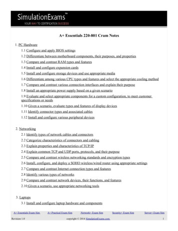
SPU-sim : A cycle accurate simulator for the SPU3execute multiple thread blocks on the same SM in order to increase performance.It is not always possible due to hardware limitations such as the shared memorysize needed by a thread block, the number of threads per thread block, etc.In the next section, we describe stencil computations and their execution onGPGPUs.2.2Stencil computations and its implementation on GPGPUsIn our case, a stencil defines the value of a rectangular grid point in a 2dimensional spatial grid at time t as a function of neighboring grid points atrecent times before t or during t. A stencil computation computes the stencil foreach grid point over time steps.The computation of such kernels can be split into tiles where each tile operates on a subset of the complete domain. Multiple tiles can be executed concurrently after mathematical transformations and proper tiling. Tiles may dependon values produced by other tiles; care must be taken to ensure that these intertile dependencies are acyclic. Each tile will then load all the data needed for itsexecution, which involves writing back the computed data in the closest memorythat is shared across all the threads. On CPUs, this level of memory will be theRandom Access Memory (RAM), and on GPGPUs it will be the global memory.When executing these tiles as thread blocks on GPGPUs, synchronization isnecessary between thread blocks to ensure that the scheduling of the blocks iscorrect [3,5]. Current GPUs do not allow synchronization between thread blocks,meaning that the type of synchronization used is not claimed to be supportedby the current generations of GPGPUs and might not even work on futuregenerations. In addition to that, the global memory used to store the data forthe computation and the synchronization between thread blocks is slow, meaningthat a lot of time might be wasted waiting for the load/store unit to performthe global memory accesses.Rather than use a stencil computation for our tests we used a tiled matrixmultiplication algorithm, which exercises the same features of the simulator butis simpler to create and run.Figure 1 shows how matrix C is tiled with indices (i, j) [0, 3]2 . Each tilecomputes a subset of the final matrix C and all tiles are independent. In thisexample, tile (0, 0) will first multiply the green tile from matrix A and the redtile from matrix B. The yellow tiles from matrix C represent the tiles that needthe same tile from A and B during their computation. We can see that thesetwo input tiles are used by six other tiles than (0, 0).Assigning each tile to a thread block on GPGPUs will make every threadblock load from global memory, some data that is also loaded by a neighboringthread block. This introduces long delays and thus, a performance loss, in termsof speed and energy. On modern GPUs this performance and energy degradationis considerably mitigated by the presence of caches, but for simplicity of thediscussion, we assume a GPU platform without caches. Rajopadhye et al. claimthat even this would have a speed and energy cost that would be further reduced
4SPU-sim : A cycle accurate simulator for the SPUby the SPU, but this is also not empirically justified. The simulator developedin this project is intended to allow all these three cases to be tested.Fig. 1: Data usage in tiled matrix-matrix multiplicationIn the next section, we introduce the architecture that we simulate: a stencilspecialized GPGPU extension.3The simulated architectureThis section is organized as follows: In the first part we will introduce the globalarchitecture simulated by the SPU simulator (SPU-sim); In the second section,we discuss several programming challenges caused by obfuscation of SPU architecture from the programmer; Finally, we will describe one possible optimizationfor our simulator.3.1PrincipleThe only way for multiple thread blocks to share data on current GPGPUs is touse the global memory. If the data shared between these thread blocks does notfit in a shared level of cache, the accesses to these memory locations will resultin global memory accesses. This memory is an off chip memory that introduceslong delays for each access.In order to enable inter-SM communication, the SPU has a new kind ofmemory called Communication Buffers (CBs). These CBs are used as producer/consumer buffers between adjacent SMs. Each SM can read from its northand west buffers, and may write to its south and east buffers so that the datapropagation is limited to one direction (from NW to SE). Every SM is then
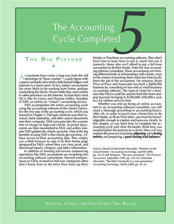
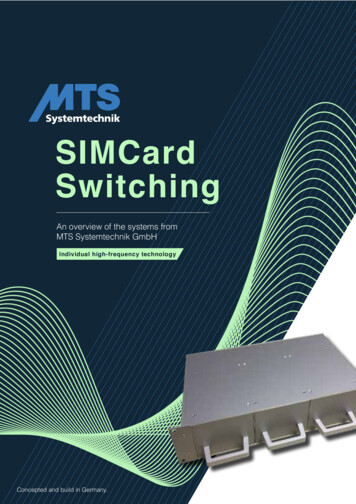
SPU-sim : A cycle accurate simulator for the SPU5related to four CBs, one in each direction. Figure 2 illustrates the data propagation between adjacent SMs on GPGPUs. The data produced by the top leftSM is written to global memory for the other neighboring SMs to be able toload it. Even though the data was locally close to the loading SMs, global memory accesses are issued. Figure 3 illustrates how the communication buffers areattached to the SMs and with arrows representing the data propagation on theSPU. Dotted boxes represent the SMs and CBs in the neighborhood of the solidline SM.Fig. 2: Data propagation for stencilcomputation on GPGPUFig. 3: CBs attachment to SMs anddata propagation on the SPUTo ensure that the data is written by the producer before the consumerreads it, a SPU-wide barrier through all the SMs is introduced. We call it ablock synchronization. We refer to time step as the computation between twoblock synchronizations. Figure 4 shows how synchronization issues are avoidedby splitting the CBs into two distinct memories. At time step N the SM1 writesin CB1 while SM2 reads from CB2. A block synchronization make the SMs toswitch buffers so that at time step N 1, SM1 writes in CB2 and SM2 readsfrom CB1. This synchronization ensures that the data is produced before it isconsumed. We consider this pair of buffers to be the single, unique CB for therest of this report.For the rest of this example, let’s consider that we have a four by four grid ofSMs. As GPGPU programming hides the actual architecture from the programmer through virtualization, so does the SPU. The programmer might launch an8 8 grid of threads blocks of the SPU, which means that there are more threadblocks than the number of SMs. In order to perform the computation correctly,the run-time system of the SPU will then have to go through multiple passes.Figure 5 shows how the grid of thread blocks is split into four passes for thisexample. We identify a thread block by three coordinates i, j, which are its row
6SPU-sim : A cycle accurate simulator for the SPUFig. 4: CBs Accesses by two SMs at two consecutive time steps (separated bythe red bar)and column number in its containing pass and by k, which determines its passnumber. The thread block A is then (0, 0, 0), B is (3, 0, 1), C is (1, 2, 2) and D is(0, 0, 3).The programmer would then select the blocks that are on the frontiers of itsgrid to load and store data from global memory. All the interior blocks wouldjust transfer data to their neighbors through the CBs. Meaning that the blocksaccessing global memory would be the following: k 0, (j 0, i [0, 3]) (i 0, j [0, 3]) k 1, (j 0, i [0, 3]) (i 3, j [0, 3])(i, j, k),k 2, (j 3, i [0, 3]) (i 0, j [0, 3]) k 3, (j 3, i [0, 3]) (i 3, j [0, 3])Fig. 5: Grid of thread blocks split intomultiple passes on SPU-simFig. 6: Hardware placement of SMsand IUs (SMs are squares, IUs are triangles)During the execution of pass 1, the thread block (1, 0, 1) for example, wouldexpect to read its data from its west neighbor, but it won’t be able to readthe correct data as (1, 3, 0) already finished its execution. The SPU virtualization mechanism shields the programmer from having to determine which thread
SPU-sim : A cycle accurate simulator for the SPU7blocks are on the borders of the grid so that they load data from global memory and thus, execute a different code than the rest of the SMs. This is whythe SPU model introduces the Interface Units (IUs). These IUs are simplifiedSMs, placed on all sides of the hardware grid of SMs, and their purpose is onlyto load/store data from global memory and write it into their CBs. Figure 6,shows their placement and their identification number. Each IU is identified byits direction (north, east, south, west) and an id starting from the north-west.For example, the id of IU number 22 is 2 at pass 0, and the id of IU 29 is 5 atpass 3 and 1 at pass 1. As IUs are simplified SMs, if a pass doesn’t fill the entirehardware grid, then a SM can act as an IU.The programmer therefore assumes an unlimited grid of thread blocks, surrounded by IUs. This way, every SM expects the data to come from a CB and notfrom global memory. When (0, 0, 3) is executed, it expects data from its northand west CBs. And theses CBs will be filled by IUs. The problem is that theprogrammer was not expecting any IUs between passes as she is not aware of thearchitecture. In order to ensure the correctness of the results, we need to spill(store to global memory) the output, and restore (load from global memory) theinputs of passes that are not on the borders. This is why SPU-sim introducesVirtual IUs (VIUs).3.2Virtual IUs (VIUs)In order to allow communication between two thread blocks that are not in thesame pass, we introduce the VIUs. During a pass, if an IU is inactive becausethe thread block grid is larger than the actual architecture, this IU is turnedinto a VIU for the all pass. For example, at pass 0, IUs 28.31 and 20.23 areturned into VIUs. A VIU can then have two different purposes. It can be a:– Spilling Unit: If the VIU direction is south or east, then it is transformedinto a spilling unit. It will then, at each time step, store the entire CB thatis next to it to global memory.– Restore Unit: If the VIU direction is north or west, then it is transformedinto a spilling unit. It will then, at each time step, load an entire CB data,previously spilled, from global memory and store it to its next CB.System generated code (i.e., not written by the programmer) should be addedat compilation time, in order to manage the VIUs. This instruction, would onlyexecute if a special register, within any SM or IU is set by the run time systemat every pass. Algorithm 1 shows the type of code that would be produced bythe eventual compiler (there is no existing compiler for the SPU yet). In thisalgorithm, VIU represents a register, private to every SM and IU, which is aboolean value specifying whether it should act like a VIU. The iu dir variablerepresents is a register that is also present in every SM and IU that is set bythe run time system at every pass that can contain four values representing theVIU direction (NORTH, EAST, WEST or SOUTH). A Spill operation loads theentire CB and store it to global memory, and a Restore reads from global memory
8SPU-sim : A cycle accurate simulator for the SPUand store the corresponding data to the next CB. A block synchronization meansa SPU-wide synchronization. Finally, LAST represents a SPU register that isset to true by the run time system when all the thread blocks from the currentpass are done.if VIU thenif iu dir is NORTH or WEST thendoRestore;block synchronization;while !LAST ;else// iu dir is SOUTH or EASTdoblock synchronization;Spill;while !LAST ;endelse// Normal CodeendAlgorithm 1: Code for Virtual IUsThe VIUs will then work as long as the current pass is not completely done.The address calculation for the spilling and restoring is described in detail in theappendix. They might do some useless work by spilling CBs to global memoryeven though there is no data to save.Even though the VIUs introduces some accesses to global memory, which iswhat the SPU tries to avoid, these accesses are negligible, and also unavoidablefor the class of computation targeted. To summarize, the IUs are the interfacebetween the global memory and the CBs; the VIUs are the interface (hiddento the programmer) between two neighboring thread blocks that are executedin different passes. The next section describes how to avoid redundant restoringand spilling introduced by the VIUs.3.3Avoiding useless restoring and spillingBy reconsidering the example of figure 5, we can see that (0, 0, 3) will waitfor some data coming from (0, 3, 1) and (3, 0, 2) by doing a certain number ofblock synchronization but no effective work. As the entire pass 3 depend on(0, 0, 3), the entire pass of thread blocks will wait for a certain number N ofblock synchronization to wait for (0, 0, 3) to start its computation, plus a certainnumber M of block synchronization for the data to come from (0, 0, 3) to its CBs.When waiting for these N block synchronizations, the VIUs will spill and restoredata, which involves a lot of wasted time and energy because they are not needed
SPU-sim : A cycle accurate simulator for the SPU9and transfer useless data. In order to avoid this phenomenon, we introduce onenew register that contains a boolean value called regstart, specifying when oneof the loading IU (north or west) has started its computation. When it is thecase, regstart is set to true and the VIUs are unleashed so that they start theircomputation at the same time step than the loading IUs. The VIUs won’t startspilling and restoring before any computation. In the case of a pass that does notcontains any loading Ius, the VIUs must start their computation one time stepbefore any other SM. We avoid that by keeping track of another boolean value,private to each thread block that makes the thread block setting regstart totrue, unleashing the VIUs and executing one more block synchronization whenthe current pass does not contain any restoring VIUs.Next section will present our experiment’s method to ensure the correctnessof the simulator.4Ensuring the correctness of the simulatorFirst, we will describe the main modifications applied to the existing GPU simulator, then, we will present our experiments to ensure the correctness of thesimulator.4.1Modifications to gpgpu-simIn order to validate the SPU-sim, we extended a cycle accurate GPGPU simulator called gpgpu-sim [7]. This simulator is able to simulate multiple GPGPU architectures and execute native GPGPU assembly. We used the NVIDIA GTX480,a Fermi class architecture, and the NVIDIA API, by compiling our CUDA kernelswith nvcc and giving PTX assembly1 to gpgpu-sim. Because there is currentlyno SPU compiler available, we compiled a CUDA program in order to generatea PTX file and hand modified this file with SPU instructions. We compiled theprogram using nvcc without optimization in order to make the assembly easierto read and modify. Our CUDA code was compiled with the following commandwhich disables optimizations. Whenever nvcc uses another tool in its chain, thattool will also have optimizations disabled by the -O0 flag.nvcc O0 Xopencc O0 Xptxas O0 ptx o u r F i l e . cuA list of all our PTX extensions, and a description of how the CBs areimplemented in the simulator can be found in the appendix.Figure 7 represents the execution flow of SPU-sim. When an executablelaunched by the user includes a kernel call, this one is given to the GPGPU.When SPU-sim is configured, the kernel call and the parameters given to thekernel are catch by the simulator. The simulator then analyses a environmentvariable specifying if the user wants to execute a different PTX file than the onethat would be extracted from the kernel. It then simulates the correspondingPTX file with the given kernel read-executionhttp://docs.nvidia.com/cuda/
10SPU-sim : A cycle accurate simulator for the SPUFig. 7: Execution flow of SPU-simWhenever a call to gpgpu-sim is made, it will retrieve some information fromthe executable such as the thread block grid size or the number of threads perthread block. It will then execute the PTX provided instead of extracting it fromthe executable by setting an environment variable.We will briefly describe the modifications made to the cycle-accurate simulator, and then to the power analysis tool.Modifications to the cycle-accurate simulator The GPGPU architecturethat we modified is the NVIDIA Fermi architecture 2 . It contains 16 SMs, whereeach SM contains one Single Instruction Multiple Threads (SIMT) core. Thearchitecture is a 8 2 grid of SMs, but we modified it to be a 4 4 grid to obtaina square grid of SMs in order to reduce the numbers of IUs necessary. As theGTX480 is a 15 SMs GPU, we modified the already existing configuration file, inorder to have 16 SMs plus 16 IUs. All of the SMs and IUs beneficiates from thenew instruction allowing a SPU-wise synchronzation. This synchronization firstoccurs within the SM by invoking a SM-wide synchronization allong threads. Itthen invokes the SPU-wide synchronization, using the same type of mechanismas the one used for a thread synchronization.The CBs are implemented as an array of memories. Acting exactly as sharedmemory. When SPU-sim is called, the modified run time system sets the newregisters of all the SMs and IUs. Regarding if they are IUs, VIUs, their directionand attach them to their CBs. It then launch a pass and wait for its completion.During a pass, each SM executes a single thread block, when all the SMs aredone, then a new pass is scheduled.Modifications to the power analysis tool The simulator collects powerconsumption data using GPUWattch [8]. We modified the collection so that it2NVIDIA’s Fermi architecture whitepaper, http://www.nvidia.com/content/pdf/fermi white papers/nvidia fermi compute architecture whitepaper.pdf
SPU-sim : A cycle accurate simulator for the SPU11also collects data from the IUs and CBs. GPUWattch is an interface for usingMcPat [9] in gpgpu-sim. McPat doesn’t currently support heterogeneous cores,which are used in the SPU (IUs are different from SMs). As we have a grid of4 4 SMs, we also have 16 IUs. We then compute the power by assuming thatevery SM is associated with an IU. We then use the usual way to compute thetotal energy with GPUWattch, by multiplying by the number of cores by theenergy computed for one couple SM IU.4.2Validating SPU-simTo demonstrate the correctness of the simulator, we wrote a PTX-like kernelcode for tiled matrix-matrix multiplication on SPU. The results produced bySPU-sim are the same as the one produced by a CPU, regardless the size of thematrix, the size of the tiles, the size of the grid of SMs, the data footprint or thenumber of threads.For our experiments, we considered tiled matrix-matrix multiplication, witha square matrix of size 192 192 and square tiles of size 16 16. This stencil doesnot introduce any dependency between tiles. In order to spread data through theSMs instead of the global memory, we first execute (0, 0) from figure 1 loadingone tile from A and one tile from B from its north and west CBs (previouslyloaded by the IUs). After its computation, it stores the tiles from A and B intoits south and east CBs, it then invokes a block synchronization. At this timestep, the thread blocks (0, 1) and (1, 0) will load the needed data from theirCBs, etc.We ensured that the VIUs spilling and restoring was not a bottleneck. Figure8 shows the number of cycles needed to terminate the kernel, and the averagepower consumption of the architectures considered. Every code was compiledwithout any optimization. Our experiments were considering the execution usingthe SPU without avoiding the useless spilling and restoring before the computation starts as decribed in section 3.3; the SPU with this optimization; gpgpu-simwith only 1 thread block per SM at the time and the native execution usinggpgpu-sim.We used both gpgpu-sim and gpgpu-sim with only one thread block per SMat the time to be able to give a fair comparison with the SPU that only allowsone thread block at the time per SM in the current imlementation.The little number of benchmarks is due to the lack of compiler. Every PTXfiles executed by the SPU is handwritten.We can see that the number of cycles needed to perform the computation onSPU-sim is much larger that the one on gpgpu-sim. Even with the optimizationby avoiding useless restoring and spilling before the computation starts. And thepower consumption is larger too. These results can be explained by the fact thattiled matrix multiplication might not be the best application to consider. Asthis program does not include any type of dependency across tiles, its executionon GPGPU can be split into thread blocks and benefit from its performanceswithout any need for synchronizations. On the other side, the execution of tiledmatrix multiplication on the SPU introduces a lot of block synchronization to
12SPU-sim : A cycle accurate simulator for the SPUFig. 8: Larger number of cycles needed and power consumption for tiled matrixmatrix multiplication computation on the SPU than on gpgpu-simallow data propagation between SMs. As the SPU is designed to perform wellon stencils codes with data dependencies across tiles, matrix multiplication donot benefit from any advantage from the SPU.The current implementation SPU-sim can be greatly optimized, in the nextsection, we describe some of them that can be done.5Further optimizationsAs SPU-sim is at its very beginning state, we describe several optimizations thatcan be applied to the current implementation.Don’t use reduced SMs for IUsOur current IUs are SMs in which we removed the following parts:– The shared memory: The shared memory is no used to transfer data fromglobal memory to CB or from CB to global memory– L1 cache: As the L1 cache is associated to the shared memory and that theshared memory is not present in the IUs anymore, we removed the L1 caches– Special Function Unit (SFU): The SFU is made to perform complexoperations in 1 clock cycle (e.g. cosinus, sinus, square root) with a loss inprecision. None of the operations provided by the SFU is needed by the IUsso we removed it too– Floating Point Unit (FPU): The FPU is the unit that allows to docomplex and precise calculations over floating points operations. There isno need of FPU when computing memory addresses.Even with these parts removed, there is still a lot of parts, like the SIMTunits that deals with a large area on chip and some useless energy consumption.A further optimization would be to use DMAs[6] instead of our IUs as the DMAsare less complex and thus consume less power.
SPU-sim : A cycle accurate simulator for the SPU13Dummy block synchronizationWe introduced in section 3.3 the mechanism in order to avoid dummy spill andrestores. But this can be further optimized. We could avoid doing the blocksynchronizations involving no computation. This would involve determining theschedule of the thread blocks statically or to ask for a thread blocks scheduleto the programmer, and thus, to launch pass 3 at block synchronization numberN 1 to avoid many dummy block synchronization.We could also try to use the same mechanism than in section 3.3 at the end ofthe thread block computation. Every thread block will perform the total numberof block synchronization needed for the entire execution. So, even if we avoidthe useless spilling and restoring before the computation starts, we still have notyet implemented the same mechanism for the end of computation. This is morecomplex to avoid because the first pass determines the total number of blocksynchronization needed for the entire computation (at the hardware level). Andthis number is today needed to perform the address calculation for the VIUs. Ifthis address calculatio is done differently, we could keep track of a counter thatwould be incremented every time a thread block finishes, and when this value isgreater than the total number of thread blocks launched, then the VIUs wouldonly perform block synchronizations.1D-Grid supportOur current implementation of SPU-sim only supports 2D-Grid of thread blocks,but a modification to the run time system could allow 1D-grid of thread blocks.It would give more flexibility to the programmer. Figure 9 shows one exampleof data propagation for a 1D-grid of thread blocks. Whenever the programmerdecides that a thread block will write to a CB, the run time system redirect thewrite operation to the correct CB considering the implementation.Another advantage of using 1D grid of thread blocks is to be able to mapmultiple thread blocks to the same SM. This technique is widely used in GPGPUsto hide memory latencies and to overlap instructions in order to get betterperformance. This run time decision has been completely disabled for SPU.Figure 10 shows how two thread blocks can be mapped to the same SM, usinga part of shared memory to act like a CB. In this example, we only considertwo thread blocks, but this number can be greater as long as the architectureconstraints are not met and that there is enough shared memory available tobe used as virtual CBs. The run time system would then redirect the writesoperations from the thread block A to its CB to shared memory. Following thesame mechanism, read operation from thread block
Abstract.In this report, we describe the implementation of a simulatorfor a GPGPU extension model called the Stencil Processing Unit (SPU).We explain the features of the SPU that are currently implemented as anextension to an existing GPGPU simulator calledgpgpu-sim. To ensurethe correctness of our simulator, we used the tiled matrix multiplicat.