Transcription
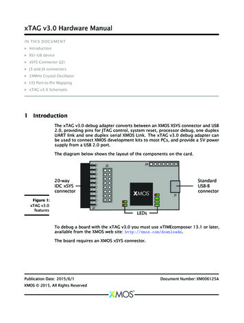
xTAG v3.0 Hardware ManualIN THIS DOCUMENT· Introduction· XS1-U8 device· xSYS Connector (J2)· J3 and J4 connectors· 24MHz Crystal Oscillator· I/O Port-to-Pin Mapping· xTAG v3.0 Schematic1IntroductionThe xTAG v3.0 debug adapter converts between an XMOS XSYS connector and USB2.0, providing pins for JTAG control, system reset, processor debug, one duplexUART link and one duplex serial XMOS Link. The xTAG v3.0 debug adapter canbe used to connect XMOS development kits to most PCs, and provide a 5V powersupply from a USB 2.0 port.The diagram below shows the layout of the components on the card.J3J420-wayIDC xSYSconnectorFigure 1:xTAG v3.0featuresJ1StandardUSB-BconnectorJ2LEDsTo debug a board with the xTAG v3.0 you must use xTIMEcomposer 13.1 or later,available from the XMOS web site: http://xmos.com/downloads.The board requires an XMOS xSYS connector.Publication Date: 2015/6/1XMOS 2015, All Rights ReservedDocument Number: XM006125A
xTAG v3.0 Hardware Manual22/8XS1-U8 deviceThe xTAG v3.0 is based on a single XS1-U8 device in a BGA package. The XS1-U8consists of a single xCORE, which comprises a multicore microcontroller withtightly integrated general purpose I/O pins and 64 KBytes of on-chip RAM. Thepins are brought out of the package and connected to the card’s components asfollows:· USB Connector (J1) The xTAG v3.0 uses a Standard B-type micro USB connectorto link to a PC. The USB connector is connected to the XS1-U8 device.· xSYS 20-way IDC headerThe processor has ports that are directly connected to the I/O pins. Six LEDs aredriven by the debugger, their function (clockwise, starting from the power buttonon the bottom right):PowerGreenThe xTAG is powered onRunGreenRedTarget is runningTarget is in debug mode and stoppedStatusGreenTarget stop reason is expected e.g. breakpoint,print messageTarget stop reason is unexpected e.g. exceptionRedTargetGreenRed3Target device is detected after a Run Configurationor Debug Configuration is used (xrun or xgdbcommand)Target device is not detected after a RunConfiguration or Debug Configuration is used(xrun or xgdb command)xSCOPEGreen FlashingOffxSCOPE is enabledNo xSCOPEJTAGGreenOffThere is JTAG activity with the target happeningNo JTAGxSYS Connector (J2)The xTAG v3.0 includes an xSYS 20-way IDC header, which can be used to connectit to an XMOS development board for debugging programs on the hardware.The xSYS connector provides pins for JTAG control, system reset, processor debug,a duplex UART link and a 2-bit serial xCONNECT Link.XM006125A
xTAG v3.0 Hardware Manual3/8PinSignalDirectionDescription15VTarget to HostPower2NCN/ANo connection3MSELHost to TargetSelect boot from JTAG - Active Low4GNDN/AGround5TDSRCHost to TargetJTAG Test Data6XL1 UP1Target to HostxCONNECT Link7TMSHost to TargetJTAG Test Mode Select8GNDN/AGround9TCKHost to TargetJTAG Test Clock10XL1 UP0Target to HostxCONNECT Target to HostJTAG Test Data14XL1 DN0Host to TargetxCONNECT Link15RST NHost to TargetSystem Reset - Active Low16GNDN/AGround17UART RXHost to TargetSerial Port18XL1 DN1Host to TargetxCONNECT Link19UART TXTarget to HostSerial Port20GNDN/AGroundThe routing of these I/O pins along with the power pins is shown below.3.1xCONNECT Link configurationSome of the I/O pins on the processor are configured as a duplex 2-bit serialxCONNECT Link. The mapping of xCONNECT Link to the pins is shown in the tablebelow:XM006125A
xTAG v3.0 Hardware Manual1Figure 2:xTAG v3.0xSYS pinout4/82NCGNDXL1 UP1GNDXL1- SNKRST NUART RXUART TX19 20PinxCONNECT LinkX0D52XL1 UP1X0D53XL1 UP0X0D54XL1 DN0X0D55XL1 DN13.2JTAG ConfigurationSome of the I/O pins on the microcontroller are driven by the JTAG signals. Themapping of the signals to the pins is shown in the table P1F0TDSNKX0D22P1G0TMSX0D10P1C0TCKX0D70P32A19MSEL
xTAG v3.0 Hardware Manual3.35/8System ResetThe system reset signal is mapped to a 1-bit port on the processor as describedbelow. It is used as an output to reset the target processor from the debugger4PinPortProcessorX0D50P32A1RST NJ3 and J4 connectorsThe xTAG v3.0 has two additional connectors. These are reserved for future use.524MHz Crystal OscillatorThe XS1-U8 is clocked at 24MHz by a crystal oscillator on the card. The processoris clocked at 500MHz and the I/O ports at 100MHz, by an on-chip phase lockedloop (PLL).XM006125A
xTAG v3.0 Hardware Manual66/8I/O Port-to-Pin MappingThe table below provides a full description of the port-to-pin mappings describedthroughout this document.PinProcessor8b32bX0D0P1A0UART 22XM006125APort1bP1G0TMSX0D50P32A1RST NX0D51P32A2DBGX0D52P32A3XL1 UP1X0D53P32A4XL1 UP0X0D54P32A5XL1 DN0X0D55P32A6XL1 DN1X0D69P32A19UART DNX0D70P32A20MSEL
PIU10E5PIU10H1PIU10M2PIU10M1XT3 C1205VCOD6D6ADC 02GNDPIC401PIC40222UCOC4C41V86PIR606ADC 1V03V3XT3 DNFXT3 DNF34PIR604COR6C10K R6CPIR60312PIR602COR6B10K R6BPIR601COSW1SW1XT3 DNFGNDCOC10C102PCOC6C63V3ANLUSB0DPUSB DPNLUSB0DNUSB DNA2B2A3B3ADC IN0ADC IN1ADC IN2ADC IN3AVDDH2NCG2NCL3NCB4NCA4PIU10A4 NCL5MODE0L4MODE1B5MODE2B6MODE3F2PIU10F2 OSC EXT NB1TDOD2TDID1PIU10D1 TMSC1PIU10C1 D701PIR5023V3COR5COD7D7A5USB DPA6USB DNA7PIU10A7 USB VBUSB7PIU10B7 USB IDPIU10A6PIU10A5COU1BU1BE2PIU10E2 DEBUG NRST N LOCPIU10C2C2RST NTDO LOCTDI LOCTMS LOCTCK LOCMSEL IR8018PIR8087PIR8076PIR8065PIR8053V3PISW102AXT3 DNFKSC421JXT3 DNFPISW101A1A1BPISW101BPIR70110KGNDPIMTH101COR7R7 PIR702ADC IN2NLADC0IN0ADC IN0NLADC0IN1ADC IN1BUTCOMTH1MTH1PTH M3SMBJ5.0AXT3 DNFGNDPIL202PIL102GNDPID501PID601PID502 SMBJ5.0A 0RXXAPIFB102PIU10M6XS1 U8A VDDIOVDDIOADC IFB101COC11C11GNDPIC10PIC102ADC VPPIU402IN POUT5IN N4PIU405ADC IN1 NXT3 DNFINA214COU4U4PIU404ADC IN1 PGNDREFGNDPIU2022OUTVPGNDVOUT2IN N5ADC IN0 NIN PINA214COU2U2MIC5321BYPENVOUT1PIJ103GND12USB DN3USB C16PIU3016VINCOU3U3PIU306ADC IN0 P5VVBUSDD IDGNDUSB HPIJ108XT3 DNFXT3 DNFADC IN2PIJ107XT3 DNFXM006125AXT3 DNFFigure 3:xTAG 1 U8A 0D58X0D43/WAKEGREENA9B9XL UP0XL UP1SRST NDBGNLBUTBUTDIG IN0TDSRCDIG D7LED7LED2LED3TMSUART 11J12PIU10J12K11PIU10K11K12UART N00PADC IN0 PNLADC0IN00NADC IN0 NNLADC0IN10PADC IN1 PNLADC0IN10NADC IN1 NNLADC0IN2ADC IN2NLADC0IN3ADC IN3NLDIG0IN0DIG IN0NLDIG0IN1DIG PIR402PIR302PIR202XL DN0XL 67PIJ407PIJ403PIJ402PIJ401NACOJ4J4NLXL0DN1XL DN1NLXL0DN0XL DN0NLXL0UP0XL UP0NLXL0UP1XL UP1NLLED3LED3NLLED2LED2NLLED1LED1NLLED0LED0Sheet 1 of 1xTAG3Sheet NameXTAG3.PrjPCBProject NameCopyright XMOS Ltd 2012GNDNLTDO0LOCTDO LOCNLTDI0LOCTDI LOCNLTCK0LOCTCK LOCNLTMS0LOCTMS LOCNLMSEL0LOCMSEL LOCNLRST0N0LOCRST N LOCGNDFEM HEADER RANLMSELMSEL3PIJ203NLTDSRCTDSRC 2011NLTDSNKTDSNK PIJ201313NLSRST0NSRST N PIJ201515NLUART0DNUART DNPIJ201717NLUART0UPUART UPPIJ201919Date CCOR1DR1D470R470R470R470RPIF101IDC HEADER MALXT3 1087PIR1076PIR1065PIR1053V3Rev1V2B7PIJ106xTAG v3.0 Hardware Manual7/8xTAG v3.0 Schematic
xTAG v3.0 Hardware Manual8/8Copyright 2015, All Rights Reserved.Xmos Ltd. is the owner or licensee of this design, code, or Information (collectively, the “Information”) andis providing it to you “AS IS” with no warranty of any kind, express or implied and shall have no liability inrelation to its use. Xmos Ltd. makes no representation that the Information, or any particular implementationthereof, is or will be free from any claims of infringement and again, shall have no liability in relation to anysuch claims.XM006125A
The xTAG v3.0 debug adapter converts between an XMOS XSYS connector and USB 2.0, providing pins for JTAG control, system reset, processor debug, one duplex UART link and one duplex serial XMOS Link. The xTAG v3.0 debug adapter can be used to connect XMOS development kits to most PCs, and provide a 5V power supply from a USB 2.0 port.