Transcription
EVALUATION KIT AVAILABLEMAX3421EUSB Peripheral/Host Controllerwith SPI InterfaceGeneral DescriptionThe MAX3421E USB peripheral/host controller containsthe digital logic and analog circuitry necessary toimplement a full-speed USB peripheral or a full-/lowspeed host compliant to USB specification rev 2.0. Abuilt-in transceiver features 15kV ESD protection andprogrammable USB connect and disconnect. An internal serial interface engine (SIE) handles low-level USBprotocol details such as error checking and bus retries.The MAX3421E operates using a register set accessedby an SPI interface that operates up to 26MHz. Any SPImaster (microprocessor, ASIC, DSP, etc.) can add USBperipheral or host functionality using the simple 3- or 4wire SPI interface.The MAX3421E makes the vast collection of USBperipherals available to any microprocessor, ASIC, orDSP when it operates as a USB host. For point-to-pointsolutions, for example, a USB keyboard or mouse interfaced to an embedded system, the firmware that operates the MAX3421E can be simple since only atargeted device is supported.Internal level translators allow the SPI interface to run ata system voltage between 1.4V and 3.6V. USB-timedoperations are done inside the MAX3421E with interrupts provided at completion so an SPI master does notneed timers to meet USB timing requirements. TheMAX3421E includes eight general-purpose inputs andoutputs so any microprocessor that uses I/O pins toimplement the SPI interface can reclaim the I/O pinsand gain additional ones.Featureso Microprocessor-Independent USB Solutiono Software Compatible with the MAX3420E USBPeripheral Controller with SPI Interfaceo Complies with USB Specification Revision 2.0(Full-Speed 12Mbps Peripheral, Full-/Low-Speed12Mbps/1.5Mbps Host)o Integrated USB Transceivero Firmware/Hardware Control of an Internal D Pullup Resistor (Peripheral Mode) and D /DPulldown Resistors (Host Mode)o Programmable 3- or 4-Wire, 26MHz SPI Interfaceo Level Translators and VL Input Allow IndependentSystem Interface Voltageo Internal Comparator Detects VBUS for SelfPowered Peripheral Applicationso ESD Protection on D , D-, and VBCOMPo Interrupt Output Pin (Level- or ProgrammableEdge) Allows Polled or Interrupt-Driven SPIInterfaceo Eight General-Purpose Inputs and Eight GeneralPurpose Outputso Interrupt Signal for General-Purpose Input Pins,Programmable Edge Polarityo Intelligent USB SIEo Automatically Handles USB Flow Control andDouble BufferingThe MAX3421E operates over the extended -40 C to 85 C temperature range and is available in a 32-pinTQFP package (5mm x 5mm) and a 32-pin TQFN package (5mm x 5mm).o Handles Low-Level USB Signaling DetailsApplicationso Space-Saving Lead-Free TQFP and TQFNPackages (5mm x 5mm)Embedded SystemsMedical DevicesMicroprocessors andDSPsCustom USB DevicesCamerasDesktop RoutersPLCsSet-Top BoxesPDAsMP3 PlayersInstrumentationo Contains Timers for USB Time-SensitiveOperations so SPI Master Does Not Need to TimeEventsOrdering InformationPINPACKAGEPARTTEMP RANGEMAX3421EEHJ -40 C to 85 C32 TQFPMAX3421EETJ -40 C to 85 C32 TQFN-EP*TOPMARK—BTBG*EP Exposed pad. Denotes a lead(Pb)-free/RoHS-compliant package.For pricing, delivery, and ordering information, please contact Maxim Directat 1-888-629-4642, or visit Maxim’s website at www.maximintegrated.com.19-3953; Rev 4; 7/13
MAX3421EUSB Peripheral/Host Controllerwith SPI InterfaceFeatures in Host Operationo Eleven Registers (R21–R31) are Added to theMAX3420E Register Set to Control Host Operationo Host Controller Operates at Full Speed or LowSpeedo FIFOSSNDFIFO: Send FIFO, Double-Buffered 64-ByteRCVFIFO: Receive FIFO, Double-Buffered 64-Byteo Handles DATA0/DATA1 Toggle Generation andCheckingo Performs Error Checking for All Transferso Automatically Generates SOF (Full-Speed)/EOP(Low-Speed) at 1ms Intervalso Automatically Synchronizes Host Transfers withBeginning of Frame (SOF/EOP)Features in Peripheral Operationo Built-In Endpoint FIFOSEP0: CONTROL (64 bytes)EP1: OUT, BULK or INTERRUPT, 2 x 64 Bytes(Double-Buffered)EP2: IN, BULK or INTERRUPT, 2 x 64 Bytes(Double-Buffered)EP3: IN, BULK or INTERRUPT (64 Bytes)o Double-Buffered Data Endpoints IncreaseThroughput by Allowing the SPI Master toTransfer Data Concurrent with USB Transferso SETUP Data Has its Own 8-Byte FIFO, SimplifyingFirmwareTypical Application Circuitso Reports Results of Host Requests3.3VREGULATORo Supports USB Hubso Supports ISOCHRONOUS Transferso Simple ProgrammingSIE Automatically Generates Periodic SOF(Full-Speed) or EOP (Low-Speed) FrameMarkersSPI Master Loads Data, Sets Function Address,Endpoint, and Transfer Type, and Initiates theTransferMAX3421E Responds with an Interrupt andResult Code Indicating Peripheral ResponseTransfer Request Can be Loaded Any TimeSIE Synchronizes with Frame MarkersFor Multipacket Transfers, the SIEAutomatically Maintains and Checks theData Toggles2USBMAX3421ESPI3, 4INTμPFigure 1. The MAX3421E Connects to Any MicroprocessorUsing 3 or 4 Interface PinsThe MAX3421E connects to any microprocessor (µP)using 3 or 4 interface pins (Figure 1). On a simplemicroprocessor without SPI hardware, these can bebit-banged general-purpose I/O pins. Eight GPIN andeight GPOUT pins on the MAX3421E more thanreplace the µP pins necessary to implement the interface. Although the MAX3421E SPI hardware includesseparate data-in (MOSI, master-out, slave-in) and dataout (MISO, master-in, slave-out) pins, the SPI interfacecan also be configured for the MOSI pin to carry bidirectional data, saving an interface pin. This is referredto as half-duplex mode.Maxim Integrated
MAX3421EUSB Peripheral/Host Controllerwith SPI InterfaceTypical Application Circuits (continued)3.3VREGULATORPOWER RAILMAX3421EUSBSPI3, 4INTTwo MAX3421E features make it easy to connect tolarge, fast chips such as ASICs and DSPs (Figure 2).First, the SPI interface can be clocked up to 26MHz.Second, the VL pin and internal level translators allowrunning the system interface at a lower voltage thanthe 3.3V required for VCC.ASIC,DSP,ETC.Figure 2. The MAX3421E Connected to a Large OINTMICROASICDSPSCLKMOSISSLOCALGNDThe MAX3421E provides an ideal method for electricallyisolating a USB interface (Figure 3). USB employs flowcontrol in which the MAX3421E automatically answershost requests with a NAK handshake, until the microprocessor completes its data-transfer operations overthe SPI port. This means that the SPI interface can runat any frequency up to 26MHz. Therefore, the designeris free to choose the interface operating frequency andto make opto-isolator choices optimized for cost or performance.Figure 3. Optical Isolation of USB Using the ULTMICRO,ASIC,DSPSPI3, 4INTVBUSMAX3421EUSB"A"D D-USBUSB"B" PERIPHERALGNDFigure 4. The MAX3421E in an Embedded Host ApplicationMaxim IntegratedFigure 4 shows a block diagram for a system in whichthe MAX3421E operates as a USB host. A USB hostsupplies 5V power to the VBUS pin of the USB “A” connector to power USB peripherals. A system that provides power to an external peripheral should useprotection circuitry on the power pin to prevent anexternal overcurrent situation from damaging the system. A VBUS switch, such as the MAX4789, providespower control plus two additional features: it limits thecurrent delivered to the peripheral (for example to200mA), and it indicates a fault (overcurrent) conditionto the SPI controller. Maxim offers a variety of VBUSswitches with various current limits and features.Consult the Maxim website for details.A 3.3V regulator (for example, the MAX6349TL) powersthe MAX3421E, and optionally the system controller. Ifthe system controller operates with a lower voltage, theMAX3421E SPI and I/O interface can run at the lowervoltage by connecting the system voltage (for example, 2.5V or 1.8V) to the MAX3421E VL pin.3
MAX3421EUSB Peripheral/Host Controllerwith SPI InterfaceFunctional DiagramRESXIXOVCCINTERNALPORRESETLOGICOSCAND4x PLL1.5kΩPOWERDOWND D-USB SSINTENDPOINTBUFFERSVBCOMPVLSPI SLAVEINTERFACEESDPROTECTIONVBUS 71V TO PXMaxim Integrated
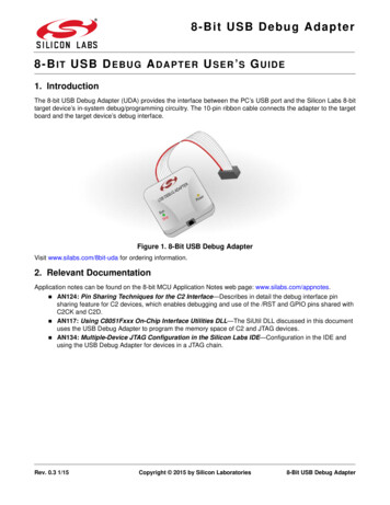
MAX3421EUSB Peripheral/Host Controllerwith SPI InterfacePin urpose Input. GPIN7–GPIN0 are connected to VL with internal pullup resistors.GPIN7–GPIN0 logic levels are referenced to the voltage on VL.2VLInputLevel-Translator Voltage Input. Connect VL to the system’s 1.4V to 3.6V logic-level powersupply. Bypass VL to ground with a 0.1µF capacitor as close to VL as possible.3, ose Push-Pull Outputs. GPOUT7–GPOUT0 logic levels are referenced to thevoltage on VL.12RESInputDevice Reset. Drive RES low to clear all of the internal registers except for PINCTL (R17),USBCTL (R15), and SPI logic. The logic level is referenced to the voltage on VL. (See theDevice Reset section for a description of resets available on the MAX3421E.) Note: TheMAX3421E is internally reset if either VCC or VL is not present. The register file is not accessibleunder these conditions.13SCLKInputSPI Serial-Clock Input. An external SPI master supplies SCLK with frequencies up to 26MHz. Thelogic level is referenced to the voltage on VL. Data is clocked into the SPI slave interface on therising edge of SCLK. Data is clocked out of the SPI slave interface on the falling edge of SCLK.14SSInputSPI Slave Select Input. The SS logic level is referenced to the voltage on VL. When SS is drivenhigh, the SPI slave interface is not selected, the MISO pin is high impedance, and SCLKtransitions are ignored. An SPI transfer begins with a high-to-low SS transition and ends with alow-to-high SS transition.15MISOOutputSPI Serial-Data Output (Master-In Slave-Out). MISO is a push-pull output. MISO is tri-stated inhalf-duplex mode or when SS 1. The MISO logic level is referenced to the voltage on VL.16MOSIInput orInput/OutputSPI Serial-Data Input (Master-Out Slave-In). The logic level on MOSI is referenced to thevoltage on VL. MOSI can also be configured as a bidirectional MOSI/MISO input and output.(See Figure 15.)17GPXOutputGeneral-Purpose Multiplexed Push-Pull Output. The internal MAX3421E signal that appears onGPX is programmable by writing to the GPXB and GPXA bits of the PINCTL (R17) register and theSEPIRQ bit of the MODE (R27) register. GPX indicates one of five signals (see the GPX section).18INTOutputInterrupt Output. In edge mode, the logic level on INT is referenced to the voltage on VL and isa push-pull output with programmable polarity. In level mode, INT is open-drain and active low.Set the IE bit in the CPUCTL (R16) register to enable INT.20D-Input/OutputUSB D- Signal. Connect D- to a USB connector through a 33Ω 1% series resistor. Aswitchable 15kΩ D- pulldown resistor is internal to the device.Maxim Integrated5
MAX3421EUSB Peripheral/Host Controllerwith SPI InterfacePin Description (continued)6PINNAMEINPUT/OUTPUT21D Input/OutputFUNCTIONUSB D Signal. Connect D to a USB connector through a 33Ω 1% series resistor. Aswitchable 1.5kΩ D pullup resistor and 15kΩ D pulldown resistor is internal to the device.22VBCOMPInputVBUS Comparator Input. VBCOMP is internally connected to a voltage comparator to allow theSPI master to detect (through an interrupt or checking a register bit) the presence or loss ofpower on VBUS. Bypass VBCOMP to ground with a 1.0µF ceramic capacitor. VBCOMP is pulleddown to ground with RIN (see Electrical Characteristics).23VCCInputUSB Transceiver and Logic Core Power-Supply Input. Connect VCC to a positive 3.3V powersupply. Bypass VCC to ground with a 1.0µF ceramic capacitor as close to the VCC pin as possible.24XIInputCrystal Oscillator Input. Connect XI to one side of a parallel resonant 12MHz 0.25% crystaland a load capacitor to GND. XI can also be driven by an external clock referenced to 1GPIN532GPIN6—EPCrystal Oscillator Output. Connect XO to the other side of a parallel resonant 12MHz 0.25% crystaland a load capacitor to GND. Leave XO unconnected if XI is driven with an external source.InputGeneral-Purpose Inputs. GPIN7–GPIN0 are connected to VL with internal pullup resistors.GPIN7–GPIN0 logic levels are referenced to the voltage on VL.InputExposed Pad, Connected to Ground. Connect EP to GND or leave unconnected. EP is located onthe bottom of the TQFN package. The TQFP package does not have an exposed pad.Maxim Integrated
MAX3421EUSB Peripheral/Host Controllerwith SPI InterfaceRegister DescriptionThe SPI master controls the MAX3421E by reading andwriting 26 registers in peripheral mode (see Table 1) orreading and writing 23 registers in host mode (see Table2). Setting the HOST bit in the MODE (R27) register configures the MAX3421E for host operation. When operatingas a USB peripheral, the MAX3421E is register-compatible with the MAX3420E with the additional features listedin Note 1b below Table 1. For a complete description ofregister contents, refer to the MAX3421E ProgrammingGuide on the Maxim website.A register access consists of the SPI master first writingan SPI command byte followed by reading or writing thecontents of the addressed register. All SPI transfers areMSB first. The command byte contains the registeraddress, a direction bit (read 0, write 1), and theACKSTAT bit (Figure 5). The SPI master addresses theMAX3421E registers by writing the binary value of theregister number in the Reg4 through Reg0 bits of thecommand byte. For example, to access the IOPINS1(R20) register, the Reg4 through Reg0 bits would be asfollows: Reg4 1, Reg3 0, Reg2 1, Reg1 0, Reg0 0. The DIR (direction) bit determines the direction forthe data transfer. DIR 1 means the data byte(s) arewritten to the register, and DIR 0 means the databyte(s) are read from the register. The ACKSTAT bit setsthe ACKSTAT bit in the EPSTALLS (R9) register (peripheral mode only). The SPI master sets this bit to indicatethat it has finished servicing a CONTROL transfer. Sincethe bit is frequently used, having it in the SPI commandbyte improves firmware efficiency. The ACKSTAT bit isignored in host mode. In SPI full-duplex mode, theMAX3421E clocks out eight USB status bits as the com-mand byte is clocked in (Figures 6, 7). In half-duplexmode, these status bits are accessed as register bits.The first five registers (R0–R4) address FIFOs in bothperipheral and host modes. Repeated accesses to theseregisters freeze the internal register address so that multiple bytes may be written to or read from a FIFO in thesame SPI access cycle (while SS is low). Accesses toregisters R5–R19 increment the internal register addressfor every byte transferred during the SPI access cycle.Accessing R20 freezes access at that register, accessing R21–R31 increments the internal address, andrepeated accesses to R31 freeze at R31.The register maps in Table 1 and Table 2 show whichregister bits apply in peripheral and host modes.Register bits that do not apply to a particular mode areshown as zeros. These register bits read as zero valuesand should not be written to with a logic 1.Register Map in Peripheral ModeThe MAX3421E maintains register compatibility with theMAX3420E when operating in USB peripheral mode(MAX3421E HOST bit is set to 0 (default)). Firmwarewritten for the MAX3420E runs without modification onthe MAX3421E. To support new MAX3421E features,the register set includes new bits, described in Note 1bat the bottom of Table 1.Register Map in Host ModeAs Table 2 shows, in host mode (HOST 1), someMAX3420E registers are renamed (for example R1becomes RCVFIFO), some are not used (shown withzeros), and some still apply to host mode. In addition, 11registers (R21–R31) add the USB host RACKSTAT**The ACKSTAT bit is ignored in host mode.Figure 5. SPI Command ByteSTATUS BITS (PERIPHERAL RQIN2BAVIRQOUT1DAVIRQOUT0DAVIRQIN0BAVIRQFigure 6. USB Status Bits Clocked Out as First Byte of Every Transfer in Peripheral Mode (Full-Duplex Mode Only)STATUS BITS (HOST IRQSNDBAVIRQRCVDAVIRQRSMREQIRQBUSEVENTIRQFigure 7. USB Status Bits Clocked Out as First Byte of Every Transfer in Host Mode (Full-Duplex Mode Only)Maxim Integrated7
MAX3421EUSB Peripheral/Host Controllerwith SPI InterfaceTable 1. MAX3421E Register Map in Peripheral Mode (HOST 0) (Notes 1a, EP2DISABEP1DISABCTGEP3INCTGEP2IN CTGEP1OUT00R10 CLRTOGSR11 EPIRQR12 EPIEN0STLEP0IN RSC0RSCSUDAVIRQ IN3BAVIRQ IN2BAVIRQ OUT1DAVIRQ OUT0DAVIRQ IN0BAVIRQ RC00SUDAVIEIN3BAVIEIN2BAVIEOUT1DAVIEOUT0DAVIER13 TIRQRWUDNIRQ OSCOKIRQ RCR14 UDNIER15 USBCTLHOSCSTENVBGATECHIPRESSIGRWU00RSCR16 CPUCTLPULSEWID1 PULSEWID0R17 PINCTLPWRDOWN CONNECTIN0BAVIERSCOSCOKIE OSINTGPXBGPXARSCR18 REVISION00010011RR19 FNADDR0b6b5b4b3b2b1b0RR20 0RSCGPOUT4RSCR21 IOPINS2GPIN7GPIN6GPIN5GPIN4GPOUT7GPOUT6GPOUT5R22 NIRQ2GPINIRQ1GPINIRQ0 RSCR23 NIEN2GPINIEN1GPINIEN0 RSCR24 GPINPOLGPINPOL4 GPINPOL3GPINPOL2GPINPOL1GPINPOL0 RSCGPINPOL7GPINPOL6GPINPOL5R25 —000R26 —00R27 MODE00R28 —0R29 —R30 —R31 �00000000—00000000—HOST 0 RSCNote 1a: The acc (access) column indicates how the SPI master can access the register.R read, RC read or clear, RSC read, set, or clear.Writing to an R register (read only) has no effect.Writing a 1 to an RC bit (read or clear) clears the bit.Writing a zero to an RC bit has no effect.8Maxim Integrated
MAX3421EUSB Peripheral/Host Controllerwith SPI InterfaceTable 1. MAX3421E Register Map in Peripheral Mode (HOST 0) (Notes 1a, 1b) (continued)Note 1b: In peripheral mode, the MAX3421E performs identically to the MAX3420E with the following enhancements:1) R16 adds the PULSEWID0 and PULSEWID1 bits to control the INT pulse width in edge interrupt mode(see Figure 12.) These bits default to the MAX3420E setting of 10.6µs.2) R21 adds four more GPIO bits.3) R22 and R23 add general-purpose input pins to the interrupt system. R24 controls the edge polarity.4) R27 controls the peripheral/host mode and the SEPIRQ bit.5) When [GPXB:GPXA] [1:0] and the bit SEPIRQ 1 (R27 bit 4), the GPX output replaces the BUSACTsignal with a second IRQ pin dedicated to the GPIN pin interrupts.Table 2. MAX3421E Register Map in Host Mode (HOST 1) (Note 000—R10 —00000000—R11 —00000000—R12 —00000000—R13 USBIRQ0VBUSIRQNOVBUSIRQ0000OSCOKIRQRCR14 USBIEN0VBUSIENOVBUSIE0000OSCOKIERSCR15 USBCTL00CHIPRESPWRDOWN0000RSCR16 ELPOSINTGPXBGPXARSCR18 REVISION00010011RR19 —00000000—R20 0RSCR21 4RSCR22 NIRQ2GPINIRQ1GPINIRQ0RCR23 BUSEVENTIRQRCR17 PINCTLR24 GPINPOLR25 HIRQPULSEWID1 PULSEWID0R26 MREQIEBUSEVENTIERSCR27 PEEDHOST 1RSCR28 PERADDR0b6b5b4b3b2b1b0RSCR29 RSTBUSRSTLSR30 HXFRHSISOOUTNINSETUPEP3EP2EP1EP0LSR31 HRSLJSTATUSKSTATUSHRSLT3HRSLT2HRSLT1HRSLT0RMaxim IntegratedSNDTOGRD RCVTOGRD9
MAX3421EUSB Peripheral/Host Controllerwith SPI InterfaceTable 2. MAX3421E Register Map in Host Mode (HOST 1) (Note 2) (continued)Note 2: The acc (access) column indicates how the SPI master can access the register.R read; RC read or clear; RSC read, set, or clear; LS load-sensitive.Writing to an R register (read only) has no effect.Writing a 1 to an RC bit (read or clear) clears the bit.Writing a zero to an RC bit has no effect.Writing to an LS register initiates a host operation based on the contents of the register.XO 25GPIN0 2615MISOGPIN0 26GPIN1 2714SSGPIN1 2713SCLKGPIN2 28GPIN3 2912RESGPIN4 3011GPOUT710GPOUT6GPIN5 7GPIN6 32 TQFP(5mm x S13SCLKGPIN3 2912RESGPIN4 3011GPOUT710GPOUT69GPOUT5GPIN6 32*EPMAX3421E 12345678GPOUT4GPIN5 3124GPOUT3MAX3421EGPIN2 2810MOSIGPOUT216XO 25GPOUT117D 18GPOUT0GPX19VBCOMPINT20VCCGND21VLD-22GNDD 23XIVBCOMP24TOP VIEW OF BOTTOM LEADSGPIN7VCCTOP VIEWXIPin ConfigurationsTQFN(5mm x 5mm)*EXPOSED PAD CONNECTED TO GROUNDMaxim Integrated
MAX3421EUSB Peripheral/Host Controllerwith SPI InterfaceABSOLUTE MAXIMUM RATINGS(All voltages referenced to GND, unless otherwise noted.)VCC . -0.3V to 4VVL .-0.3V to 4VVBCOMP .-0.3V to 6VD , D-, XI, XO .-0.3V to (VCC 0.3V)SCLK, MOSI, MISO, SS, RES, GPOUT7–GPOUT0,GPIN7–GPIN0, GPX, INT .-0.3V to (VL 0.3V)Continuous Power Dissipation (TA 70 C)32-Pin TQFN (derate 21.3mW/ C above 70 C) .1702mW32-Pin TQFP (derate 13.1mW/ C above 70 C).1047mWOperating Temperature Range .-40 C to 85 CJunction Temperature . 150 CStorage Temperature Range .-65 C to 150 CLead Temperature (soldering, 10s) . 300 CSoldering Temperature (reflow) . 260 CStresses beyond those listed under “Absolute Maximum Ratings” may cause permanent damage to the device. These are stress ratings only, and functionaloperation of the device at these or any other conditions beyond those indicated in the operational sections of the specifications is not implied. Exposure toabsolute maximum rating conditions for extended periods may affect device reliability.ELECTRICAL CHARACTERISTICS(VCC 3V to 3.6V, VL 1.4V to 3.6V, TA TMIN to TMAX, unless otherwise noted. Typical values are at VCC 3.3V, VL 2.5V, TA 25 C.) (Note 3)PARAMETERSYMBOLCONDITIONSMINTYP3.3MAXUNITSDC CHARACTERISTICSSupply Voltage VCCVCC3.0Logic-Interface Voltage VLVL1.4VCC Supply CurrentICCVL Supply CurrentVCC Supply Current During IdleVCC Suspend Supply CurrentVL Suspend Supply CurrentContinuously transmitting on D and D- at12Mbps, CL 50pF on D and D- to GND,CONNECT 03.6V3.6V45mASCLK toggling at 20MHz, SS low,GPIN7–GPIN0 02.3510mAD high, D- low8.715mAICCSUSCONNECT 0, PWRDOWN 13060µAILSUSCONNECT 0, PWRDOWN 12050µAILICCIDLOGIC-SIDE I/OMISO, GPOUT7–GPOUT0, GPX,INT Output High VoltageMISO, GPOUT7–GPOUT0, GPX,INT Output Low VoltageVOHVOLILOAD 1mAVL - 0.4ILOAD 5mA, VL 2.5V (Note 4)VL - 0.45ILOAD 10mA, VL 2.5V (Note 4)VL - 0.4ILOAD -1mA0.4ILOAD -20mA, VL 2.5V (Note 4)0.6ILOAD -20mA, VL 2.5V (Note 4)0.4SCLK, MOSI, GPIN7–GPIN0, SS,RES Input High VoltageVIHSCLK, MOSI, GPIN7–GPIN0, SS,RES Input Low VoltageVILSCLK, MOSI, SS, RES InputLeakage CurrentIIL-1RGPIN10GPIN7–GPIN0 Pullup Resistor to VLV2/3 x VLVV200.4V 1µA30kΩTRANSCEIVER SPECIFICATIONSDifferential-Receiver InputSensitivityMaxim Integrated VD - VD- 0.2V11
MAX3421EUSB Peripheral/Host Controllerwith SPI InterfaceELECTRICAL CHARACTERISTICS (continued)(VCC 3V to 3.6V, VL 1.4V to 3.6V, TA TMIN to TMAX, unless otherwise noted. Typical values are at VCC 3.3V, VL 2.5V, TA 25 C.) (Note 3)PARAMETERSYMBOLCONDITIONSDifferential-Receiver CommonMode VoltageMINTYP0.8Single-Ended Receiver Input LowVoltageVILSingle-Ended Receiver InputHigh VoltageVIHMAXUNITS2.5V0.8V2.0Single-Ended ReceiverHysteresis VoltageV0.2D , D- Output Low VoltageVOLRL 1.5kΩ from D to 3.6VD , D- Output High VoltageVOHRL 15kΩ from D and D- to GNDDriver Output ImpedanceExcluding External Resistor(Note 4)2.827V0.3V3.6V11ΩD Pullup ResistorREXT 33Ω1.4251.51.575kΩD , D- Pulldown ResistorREXT 33Ω14.251515.75kΩD , D- Input Impedance300kΩESD PROTECTION (D , D-, VBCOMP)Human Body Model1µF ceramic capacitors from VBCOMP andVCC to GND 15kVIEC 61000-4-2 Air-Gap Discharge1µF ceramic capacitors from VBCOMP andVCC to GND 12kVIEC 61000-4-2 Contact Discharge1µF ceramic capacitors from VBCOMP andVCC to GND 8kVThermal-Shutdown Low-to-High 160 CThermal-Shutdown High-to-Low 140 CTHERMAL SHUTDOWNCRYSTAL OSCILLATOR SPECIFICATIONS (
the SPI port. This means that the SPI interface can run at any frequency up to 26MHz. Therefore, the designer is free to choose the interface operating frequency and to make opto-isolator choices optimized for cost or per-formance. Figure 4 shows a block diagram for a system in which the MAX3421E operates as a USB host. A USB host