Transcription
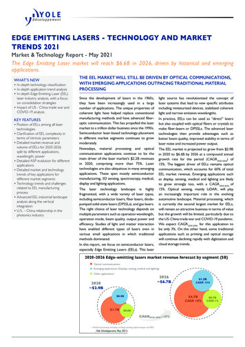
Increasing the Productivity of Laser Powder Bed Fusion for Stainless Steel316L through Increased Layer ThicknessDownloaded from: https://research.chalmers.se, 2022-08-10 19:08 UTCCitation for the original published paper (version of record):Leicht, A., Fischer, M., Klement, U. et al (2021). Increasing the Productivity of Laser Powder BedFusion for Stainless Steel 316L throughIncreased Layer Thickness. Journal of Materials Engineering and Performance, 30(1): -3N.B. When citing this work, cite the original published paper.research.chalmers.se offers the possibility of retrieving research publications produced at Chalmers University of Technology.It covers all kind of research output: articles, dissertations, conference papers, reports etc. since 2004.research.chalmers.se is administrated and maintained by Chalmers Library(article starts on next page)
ÓThe Author(s)1059-9495/ 4-3Increasing the Productivity of Laser Powder Bed Fusionfor Stainless Steel 316L through Increased LayerThicknessAlexander Leicht, Marie Fischer, Uta Klement, Lars Nyborg, and Eduard HryhaSubmitted: 4 August 2020 / Revised: 24 October 2020 / Accepted: 7 November 2020Additive manufacturing (AM) is able to generate parts of a quality comparable to those produced throughconventional manufacturing, but most of the AM processes are associated with low build speeds, whichreduce the overall productivity. This paper evaluates how increasing the powder layer thickness from20 lm to 80 lm affects the build speed, microstructure and mechanical properties of stainless steel 316Lparts that are produced using laser powder bed fusion. A detailed microstructure characterization wasperformed using scanning electron microscopy, electron backscatter diffraction, and x-ray powderdiffraction in conjunction with tensile testing. The results suggest that parts can be fabricated four timesfaster with tensile strengths comparable to those obtained using standard process parameters. In eithercase, nominal relative density of 99.9% is obtained but with the 80 lm layer thickness presenting somelack of fusion defects, which resulted in a reduced elongation to fracture. Still, acceptable yield strength andultimate tensile strength values of 464 MPa and 605 MPa were obtained, and the average elongation tofracture was 44%, indicating that desirable properties can be achieved.Keywordsadditive manufacturing, EBSD, laser powder bedfusion, productivity, stainless steel, tensile properties1. IntroductionLaser powder bed fusion (L-PBF) is a manufacturingprocess used for producing metal components by repeatedlyapplying thin layers of powder and selectively melting them ontop of one another using a high-energy laser to create the finalgeometry (Ref 1). This process allows for the fabrication ofcomplex near-net-shape parts with high accuracy and goodquality. With proper handling, it is possible to produce almostfully dense components with properties that are comparable tothose from conventional methods or, in some cases, even better(Ref 2). Different sectors, such as aerospace, energy, medical,marine engineering, and automotive, have found L-PBF to bean appealing option given its design freedom and improvedmechanical properties. However, one main challenge with LPBF is the relatively low productivity related to a low buildspeed and consequently a high manufacturing cost. Therefore,L-PBF is used primarily for high-end components, most oftenwithin the aerospace or medical industry, in which theproduction volumes are relatively small, and high costs areacceptable (Ref 3-5).Most of the research and development on the L-PBFprocessing of stainless steel 316L has so far focused onadjusting the process parameters to increase part quality, whichAlexander Leicht, Marie Fischer, Uta Klement, Lars Nyborg, andEduard Hryha, Department of Industrial and Material Science,Chalmers University of Technology, Gothenburg, Sweden. Contacte-mail: alexander.leicht@chalmers.se.Journal of Materials Engineering and Performancemeans optimizing certain areas, such as mechanical properties,relative density, and surface roughness. For example, Grecoet al. (Ref 6) revealed that similar densities can be achievedwith different volumetric energy densities as long as the laserpenetration depth is sufficiently high. Liu et al. (Ref 7) revealedthat using an increased scan speed changed the microstructure,namely the size of the cells inside the larger elongated grains.Sun et al. (Ref 8), on the other hand, maintained the volumetricenergy density at a constant 104 J/mm3 but alternated the scanspeed, hatch distance, and power and showed differences inmicrostructure and tensile properties. Furthermore, Leicht et al.(Ref 9) showed that increasing the hatch distance and scanspeed can excessively increase the number of defects. In astudy by Liverani et al. (Ref 10), it was demonstrated that thedensity decreases when the laser power is too low. However,Leicht et al. and Liverani et al. did not observe large variationsin tensile strength. Meanwhile, the work by Tsopanos et al. (Ref11) demonstrated the effect of laser power and laser exposuretime on the porosity of lattice structures. Based on the previousresearch, it is clear that the process parameters strongly affectthe microstructure, defect formation, and tensile properties.However, little attention has been given to increasing thebuild speed by alternating the process parameters. As emphasized by Babu et al. (Ref 12), the process must be furtherdeveloped for high productivity, especially for low-cost materials. Leicht et al. (Ref 9) and Sun et al. (Ref 13) both noted thatthe build speed can easily be improved by increasing the scanspeed and hatch distance, while good mechanical properties canstill be maintained. Several other studies have emphasized thatincreasing the layer thickness can be suitable for increasing theproductivity. Wang et al. (Ref 14) revealed that fully dense316L components with good tensile properties can be madewith layer thicknesses of 150 lm; however, no information onthe microstructure was provided in their study. Shi et al. (Ref15) fabricated fully dense Ti-6Al-4V parts with 200 lm layerthicknesses. Along similar lines, Ma et al. (Ref 16) fabricated
fully dense 1Cr18Ni9Ti stainless steel samples and found thatby varying the layer thickness between 60 and 150 lm, theycan establish a threshold value of approximately 80 lm layerthickness, above which decreased tensile strength was observed. Increasing the layer thickness could easily reduce theproduction time, which in turn considerably reduces the cost ofproduction. The downside is that increasing the layer thicknessmight reduce the part quality, which could result in undesirabletraits, such as reduced accuracy, increased surface roughness, orlower relative density (Ref 17-20). Nevertheless, certaincomponents are not limited by having somewhat lowerperformance in these aspects; in fact, each application has itsown requirements, and for certain applications, it is notnecessary to have full density or very good surfaces. Forexample, components that require post-treatments such asmachining will have limited surface requirements. Parts that areexposed to low and especially static loads (e.g., components forthe consumer market and chemical industry) are not significantly affected by reduced density. In fact, the automotiveindustry utilizes a large volume of powder metallurgy parts,characterized by the density level between 90 and 95% (Ref21), indicating that AM processing with a high build speed andhence lower costs can be attractive for low-scale manufacturingand spare parts for automotive industry.To use a higher layer thickness in an optimum way,acceptable levels of controllable defects must be guaranteed toensure the integrity of the end product and its requiredproperties. The aim of this study is to provide a detailedmicrostructure characterization and a mechanical propertiesanalysis for samples produced with 20 lm and 80 lm layerthicknesses, respectively. In particular, this study demonstrateshow the build rate can be increased by a factor of four. To date,no pre-developed process parameters exist for the 80 lm layerthickness, and thus an optimization of process parameters wasconducted prior to the final evaluation of the material-processproperties relationship.2. MethodGas-atomized stainless steel 316L powder with a sizedistribution of 20-53 lm was used as a feedstock material; thechemical composition of the powder is provided in Table 1 andis within the required specification from the machine provider.Samples used in this study were produced using an EOS M290system flushed with high-purity argon gas to retain the oxygencontent in the build chamber at below 0.1%. The machine isequipped with a Yb-fiber laser with a maximum nominal powerof 400 W and laser spot diameter of approximately 100 lm.The samples were produced using a stripe-scanning strategy, inwhich a 67 scan rotation was performed after each layer.The system was equipped with powder bed and opticaltomography monitoring systems, provided by EOS GmbH. Theoptical tomography (OT) system is based on an sCMOS(scientific complementary metal-oxide semiconductor) highspeed camera that observes the entire building platform at alltimes. The acquired data from the OT system represents theintegral of process radiation from the building platform over acertain time. This system allows for analyzing the homogeneityand stability of the building process.To determine the process window for manufacturingstainless steel 316L with an 80 lm layer thickness, 41 cubeswere manufactured using the process parameters provided inTable 2. The samples were sorted based on the volumetricP(in J/mm3) withenergy density (VED), defined by VED ¼ v h tpower P (W), scan speed v (mm/s), hatch distance h (mm), andlayer thickness t (mm). The VED ranged from 19 J/mm3 to77 J/mm3. Five different process parameter sets were selected(see ‘‘Productivity and Sample Selection’’ section) based on theporosity, productivity, and stability of the process. Theseprocess parameters were used to fabricate 10 tensile bars foreach set. The set of process parameters that lead to the besttensile properties and productivity was selected for a moreextensive characterization; these parameters are presented inTable 3. Figure 1 presents the drawing of the samples that werefabricated to their near-net-shape according to the ASTM E8/E8M 16a standard. Additional samples were fabricatedusing standard process parameters for a 20 lm layer thicknessdeveloped by EOS GmbH for stainless steel 316L (version1.10). All the tensile test bars were built vertically along thebuilding orientation, as presented in Fig. 1. The samples wereremoved from the build plate using a band saw and werecharacterized in an as-built condition.The microstructure was examined from a vertical section atthe center of the tensile test bars. Samples for metallographywere prepared through grinding using SiC paper and followingthe recommendation for stainless steel as provided by Struers.The cross section was polished using an MD-Mol polishingdisk with a 3-lm suspension and an MD-Chem with OP-S asthe final step. The porosity was measured on the as-polishedsamples and then analyzed by a thresholding procedure usingImageJ. Images were taken from the entire surface of severaldifferent cross sections—both parallel and perpendicular to thebuilding direction. In total, 10 images at a magnification of200 9 were obtained from each cross-section and then analyzed by a thresholding procedure using ImageJ. A light opticalmicroscope (ZEISS Axioscope 7) was used in combinationwith a FEG-SEM (Leo Gemini 1550) to evaluate the porosityand microstructure at various magnifications. The average cellTable 2 Processparametervariationsdetermining the process windowLaser powerScan speedHatch distanceStripe widthusedfor220-370 W800-2100 mm/s0.09-0.12 mm5 and 10 mmTable 1 Chemical composition of the 2.70.0613.40.040.0060.0050.3Journal of Materials Engineering and Performance
Table 3 Selected process parameters for further characterizationPowerLayer thicknessScan speedHatch distanceStripe width295 W0.08 mm800 mm/s0.12 mm10 mm3. Results and Discussion3.1 Productivity and Sample SelectionFig. 1 Schematic overview of sample dimensions and builtorientationsTable 4 Predicted build speed for the different layerthicknessesNo. of part25016Layer thickness, lmBuild speed, cm3/h208020805.423.23.614.4size was determined by following the line intercept procedureprovided in ASTM E112-13. The sizes were measured bycounting more than 1000 intercepts from 10 random SEMmicrographs from each condition. An electron backscattereddiffraction analysis (Nordlys II detector) was conducted using a20-kV acceleration voltage and a step size of 1.5 lm to evaluatethe grain morphology and crystallographic orientation. Highangle grain boundaries were defined by having a minimum of10 misorientation. The orientation maps were acquired andprocessed using the Channel 5 software. The x-ray diffraction(XRD) patterns were obtained using CrKa radiation in a BrukerAXS D8 Advance over a 2h range between 30 and 140 . TheICDD-card 00-033-0397 was used to identify the peaks.Tensile tests were conducted using an Instron 5500R tensiletesting machine, the test was performed using strain controlwith a crosshead velocity of 0.025%/s. The strain was measuredusing a clip-on extensometer with a span of 10 mm; the limitedspan corresponds to approximately 30% elongation. When thefull distance of the extensometer was reached, the tensile testwas paused, and the test was continued until fracture with loadcontrol. For this reason, stress–strain curves can only be shownat a point up to 30% elongation. It should be noted that theultimate tensile strength can still be acquired.Journal of Materials Engineering and PerformanceThe productivity of L-PBF is often limited by the timeneeded to melt and solidify the material. Therefore, theproductivity—in other words, the building speed—was evaluated as the volume of material that the process can melt pertime unit, which in this case is cm3/h. The building speed wasestimated by preparing two different build jobs with 10x10x10mm cubes using EOS print 2.5. EOS print is a commercialsoftware used to prepare the build jobs files and allows for thebuild time of a job to be simulated from the point when theoperator starts the machine. By comparing the softwareÕsestimation to the actual build time for more than 10 differentbuilds, only a minor difference (i.e., 2-3%) between thesimulated and actual times can be noted. The difference couldoriginate in various factors, such as uncertainties in thesoftware, estimations of recoating time, or the switch speedbetween scanned areas. The first build job was simulated with250 cubes and the second with 16 cubes; both jobs weresimulated using the process parameters provided in Table 3,and the results from the simulations are summarized in Table 4.The simulation results indicate that increasing the layerthickness from 20 lm to 80 lm could reduce the buildingtime to one-fourth of the original duration. It is worth notingthat standard EOS process parameters use a layer thickness of20 lm, whereas there are available process parameters by othersuppliers and published in the literature that have a larger layerthickness (e.g., 30 or 40 lm), indicating a lower build timereduction. In addition, the results reveal that increasing thebuild plate utilization (i.e., the number of parts on the buildplate) increases the building speed. The reason the buildingspeed is different depending on plate utilization is that the timefor recoating a powder layer and lowering the build plate isconstant regardless of the number of parts used for the setup. Itshould be noted that the build speed per layer is not influencedby the build height so long as the melting area is the same.Furthermore, each process parameter set used for finding theprocess window was simulated. The simulation reveals thatthere should be no specific trend between the VED and thebuild speed, as indicated by the red line in Fig. 2.To determine the process window, 41 cubes were manufactured using the approach outlined in the method section; theporosity of each sample was evaluated, and the results arepresented in Fig. 3. The graph shows that VEDs greater than30 J/mm3 generated a porosity content below 0.5%, and usingthe minimum porosity as a criterion, the optimum processwindow appears to be between 37 J/mm3 and 65 J/mm3. Morethan 15 of the process parameter sets generated a porosity levelbelow 0.1%. Two factors were used to decide between thesesamples, namely the build speed and the process stability. Theprocess stability was evaluated using the monitoring systemsavailable on the machine. From the OT analysis, the standarddeviation of the grey values (i.e., melt pool intensities) was
Fig. 2 Gray value standard deviation and build speed versusvolumetric energy densityFig. 4 Light optical images showing the morphology of theobserved defects on (a) samples produced with a 20 lm layerthickness and (b) samples produced with an 80 lm layer thicknessFig. 3Porosity versus volumetric energy densityextracted for each cube and layer. A low standard deviationindicates that the intensities throughout the sample tend to beclose to the mean, while a high standard deviation indicates awider spread of intensities within the specimen and hence a lessstable process. The average standard deviation for all layerswas calculated for each sample and is represented in Fig. 2along with a simulated build speed (simulated with 250 cubesof size 10 9 10 9 10 mm) for the 15 samples that reveal aporosity level below 0.1%.It appears that the standard deviation of the grey valuesincreases globally with an increasing VED. This observationalong with the process monitoring data indicates that theprocess becomes unstable for a VED greater than 50 J/mm3. Ahigh VED may result in keyhole mode melting which leads tothe formation of defects and a less robust process (Ref 22). Fiveparameter sets were selected with a low grey value standarddeviation and a high build speed; the results below arepresented only for the parameter set that exhibited the besttensile properties. The selected parameters resulted in an energydensity of 38 J/mm3 and the highest build rate among the 15samples. Each further characterization was conducted on thesamples that were manufactured with this parameter set (seeTable 3).3.2 DefectsFigure 4 provides two representative low-magnificationlight optical images of the two layer thicknesses. The samplesproduced with a 20 lm layer thickness possess few defects.The observed defects were gas porosities less than 5 lm indiameter, indicated by the arrows in Fig. 4a; no cracks or lackof fusion was observed in the samples produced with a layerthickness of 20 lm. For the samples produced with an 80 lmlayer thickness, more frequent and larger defects wereobserved, as presented in Fig. 4b. At a higher magnification,large defects and unmelted metal particles were observed inconjunction with gas-induced porosity. Gas porosity is commonly created by entrapped gas from the feedstock powder orfrom the entrapped gas in the bottom of the melt pools duringthe melting and solidification (Ref 16). Furthermore, severalline-type defects with lengths from around 25 to 50 lm wereobserved, as indicated by an arrow in Fig. 4b. These defectswere randomly distributed throughout the sample. Inside such adefect, traces of metal powder particles could be observed, andthe defect seemed to orient along the melt pool boundary. TheJournal of Materials Engineering and Performance
defect can most likely be attributed to a lack of fusion createdby insufficient melting. The presence of such defects introducesstress concentration sites which can be detrimental in the caseof dynamic loading. Nonetheless, the sample produced with an80 lm layer thickness reached a density of approximately99.9% based on the image analysis. Hence, even if the higherlayer thickness leads to some flat lack of fusion defects, they arenot abundant enough to affect the density value.3.3 MicrostructureFigure 5 reveals that the produced samples are characterizedby parabolic shaped melt pools, columnar grains, and a finecellular structure. The images are presented in two orientations—namely normal and parallel—with respect to thebuilding direction. Determining the exact size of the melt poolrequires a more comprehensive study. However, as observablein Fig. 5a and d, a substantial enlargement in melt pool size isobserved in the sample produced with an 80 lm layerthickness. Both the shape and size of the melt pools aredetermined by the process parameters, namely the laser power,scan speed, hatch distance, and layer thickness (Ref 23-29).The increased melt pool size is consequently formed by thedifferences in process parameters.As presented in Fig. 5c and f, both the samples producedwith 20 lm and 80 lm layer thickness present a fine cellularstructure, with average cell sizes of 0.48 0.10 lm and0.69 0.21 lm, respectively. The cell size is affected by thesolidification conditions (thermal gradient, cooling rate, andsolidification front velocity), which are determined by theprocess parameters and component geometry. Faster solidification indicates finer cellular/dendritic structure. The increase inthe cell size of the sample produced with 80 lm layer thicknessis a consequence of the slower solidification within the largermelt pools.Figure 6 displays EBSD orientation maps for the samplesproduced with different layer thicknesses; these maps wereacquired parallel to the building direction. As seen in Fig. 6a,the microstructure of the sample produced with 20 lm layerthickness is characterized by large elongated grains alignedwith the building direction. Many of the grains are extendedbeyond the layer thickness and span over several melt poolboundaries; hence, epitaxial grain growth has occurred. Furthermore, a strong preference in the 101 direction isobserved. The samples with 80 lm layer thickness exhibitedmore random crystallographic orientation with smaller and lesselongated grains, as displayed in Fig. 6b. It appears that theincreased layer thickness and lower energy density limit thegrowth and preferential orientation. When using the lowerenergy density, fewer layers are re-melted, which reduces theepitaxial growth. In Fig. 6b, the grains appear as half-circular,with an appearance similar to that of the melt pools, indicatingthat the grains nucleate from the melt pool boundaries insteadof grow in an epitaxial manner. Furthermore, the reducedenergy density indicates that the time the materials remain at anelevated temperature is decreased, which appears to result in asmaller grain size.As explained by Sun et al. (Ref 28), the melt pool shape andsize represent an essential aspect of texture development in LPBF. At the bottom of the melt pools, the cells grow parallel tothe build direction, and as the melt pool boundary becomessteeper, the texture begins to deviate from 001 (i.e.,becomes more random). At a certain point, the angle betweenthe normal and building direction is approximately 45 ,indicating that a predominant 101 texture is formed.The differences in the preferential crystallographic orientationobserved in this study can thus be related to the changes in meltpool size together with reduced epitaxial growth, since fewlayers have been re-melted.It has previously been demonstrated that dislocation densityis important for the properties of 316L produced by L-PBF (Ref2), and hence, Kernel average misorientation (KAM) mapswere developed from the EBSD measurements (see Fig. 7).Fig. 5 SEM micrographs of the microstructure along and normal to the building direction of the samples produced with a layer thickness of20 lm (a-c) and 80 lm (b-f). Two melt pools are marked in (a) and (c) to emphasize the enlarged size for the sample produced with 80 lmlayer thicknessJournal of Materials Engineering and Performance
Fig. 7 Kernel average misorientation maps of samples producedwith (a) 20 lm layer thickness and (b) 80 lm layer thicknessFig. 6 EBSD orientation maps in IPF coloring and parallel to thebuilding direction of samples produced with (a) 20 lm layerthickness and (b) 80 lm layer thicknessThe KAM maps express the local misorientation in the sample,which can be seen in the color coding of the figure; thismisorientation can then be used as an indication of a higherstrain. The local misorientation range is set to be between 0 and2 . Likewise, higher strains can be used as a qualitativemeasure for a high dislocation density (Ref 30). Molybdenumis known to segregate to the cell boundary. As the molybdenumatom is larger than the iron atom, a local stress/strain field isgenerated at the cell boundary, which might affect the strainmeasurement but also nominally increase the number ofdislocations (Ref 2, 31). As seen in Fig. 7a, the samplesproduced with 20 lm layer thickness reveal more localmisorientation compared with the samples produced with80 lm layer thickness (Fig. 7b). The results obtained fromthe KAM maps were affected by the step size, beam size, andthe location where the map was obtained; therefore, XRDstudies were conducted as a complement. Figure 8 presents thesamples with three detectable diffraction peaks, namely {111},{200}, and {220}, which is characteristic for the austenitephase (no other phases were observed). To evaluate thedislocation density, new scans were performed with a smallerstep size (0.001 ) and conducted over each specific peak. Thedislocation density was then derived by following the proce2dure demonstrated by Yin et al. (Ref 32): using q ¼ k be 2 , wheree is the full width at half maximum broadening (obtained bylinear fit), b is the Burgers vector and k 16.1. The dislocationdensities for the samples produced with 20 lm and 80 lm layerthickness were thereby estimated to be 1.9*1014 m 2 and7.2*1014 m 2, respectively. This confirms the results obtainedfrom the KAM maps (i.e., that samples produced with 20 lmlayer thickness have a higher density of dislocations thansamples produced with 80 lm layer thickness).3.4 Mechanical propertiesThe tensile properties of the produced samples are presentedin Fig. 9 and Table 5. Both samples exhibit approximately theJournal of Materials Engineering and Performance
same ultimate tensile strength (UTS), but the yield strength(YS) and elongation to fracture (ductility) are about 15% and30%, respectively, and lower for the sample produced with80 lm layer thickness. Still, the sample produced with 80 lmlayer thickness exceeds the requirements for 316L, according toASTM A240M-18 (see Table 5).The high yield strength of 316L samples produced with LPBF is explained by several microstructure features. Forexample, the dislocation movement can be hindered by grainFig. 8 The XRD patterns obtained from the as-built surface of theproduced samples, indicating a fully austenitic sample in both casesFig. 9 Tensile properties of the samples produced with 20 lm and80 lm layer thicknessboundaries (Ref 33), other dislocations (Ref 33, 34), cells (Ref35, 36), and element segregation (Ref 36). It appears that thecells are considered to be the most significant feature for thetensile properties, as they contain both dislocations andsegregated elements, effectively hindering the dislocationmovement (Ref 2, 33, 36). The smaller cell size and higherdislocation density in the samples built with 20 lm layerthickness are expected to provide a yield strength increaserelative to that for the sample with 80 lm layer thickness due tothe increased interaction of dislocation pile-up in the cellboundaries. This was also reported by Wang et al. (Ref 37) andWang et al. (Ref 2), who presented a linear dependencybetween decreasing cell size and increased tensile properties,consistent with the results presented in this study.Apart from differences in yield strength, a slight differencein the strain-hardening rate between the samples was noted (seethe black curve in Fig. 9). This could also be understood by thedecreased cell size and increased dislocation density. Initiallyhaving a higher dislocation density in the unloaded stage meansthat the samples will be saturated with new dislocations morequickly, which prevents new dislocations from nucleating. Theresistance to forming new dislocations reduces the strainhardening rate; however, as shown in both samples, strainhardening continues even at higher deformation but at asupposedly very low rate. This behavior was described byWang et al. (Ref 2) and is associated with deformation bytwinning and a cell–cell interaction. Wang et al. demonstratedthat dislocations pile-up in the cell boundaries promoteddeformation by twinning, which helped to sustain a steadystrain hardening. This steady strain hardening then improvesthe ductility by allowing dislocations to move in the twinboundaries, which retards necking. In addition, Sun et al. (Ref8) and Sinha et al. (Ref 38) demonstrated that 101 oriented grains are more favorable for twinning. It is assumed thatthe sample built with 20 lm layer thickness will deform bytwinning to the greatest extent, as the sample exhibits a er 101 texture. The observed higher yield strengthand ductility is thereby supposed to be explained by increasedtwinning and decreased cell size.However, the reduction in ductility is also associated withthe previously observed lack of fusion defects (Fig. 4b).Figure 10 presents the fracture surface of the samples producedwith both layer thicknesses. In both cases, a transgranularductile fracture is the characteristic failure mechanism, with thepresence of fine and deep dimple
Stainless Steel 316L through Increased Layer Thickness Downloaded from: https://research.chalmers.se, 2022-03-19 19:00 UTC Citation for the original published paper (version of record): Leicht, A., Fischer, M., Klement, U. et al (2021) Increasing the Productivity of Laser Powder Bed Fusion for Stainless Steel 316L through Increased Layer Thickness