Transcription
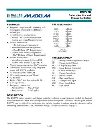
DS2770Battery Monitor andCharge ControllerFEATURESwww.maxim-ic.com§ Integrated charge controller supporting bothrechargeable lithium and NiMH batterytechnologies§ Available in two configurations:– Internal 25mW current-sense resistor– External user-selectable sense resistor§ Current measurement:– 15-bit bidirectional measurement– Internal sense resistor configuration:62.5mA LSB and 2A dynamic range– External sense resistor configuration:1.56mV LSB and 51.2mV dynamic range§ Current accumulation– Internal sense resistor: 0.25mAh LSB– External sense resistor: 6.25mVh LSB§ Voltage measurement with 4.88mV resolution§ Temperature measurement using integratedsensor with 0.125 C resolution§ 40 bytes of lockable EEPROM§ 16 bytes of general-purpose SRAM§ 42-day timer§ Dallas 1-Wireâ interface with 64-bit ID§ 1.8V logic levels§ Low power consumption:– Active current:80mA typical– Sleep current:0.5mA typicalPIN VSSSNS611VSSNC710NCIS289IS1DS277016-Pin TSSOPPIN DESCRIPTIONUVCCVCHSNSIS2IS1VSSDQVINVDDNC– Battery-Undervoltage Detect Output– Charge-Control Output– Charge-Supply Input– Sense Resistor Connection– Current-Sense Input– Current-Sense Input– Device Ground– Data Input/Output– Voltage-Sense Input– Power Supply Input– No ConnectDESCRIPTIONThe DS2770 battery monitor and charge controller performs several functions needed for thoroughbattery maintenance. When used in conjunction with the host system’s processor, a battery-pack residentDS2770 may be utilized for applications that include charging, remaining capacity estimation, safetymonitoring, and nonvolatile (NV) parametric storage. Description continued on page 2.1-Wire is a registered trademark of Dallas Semiconductor.1 of 27052605
DS2770ORDERING INFORMATIONORDERING NUMBERDS2770AE DS2770BE DS2770AE T&RDS2770BE T&RDS2770AE 025DS2770BE 025DS2770AE 025/T&RDS2770BE R2770EBR2770EAR2770EBRDESCRIPTIONTSSOP, Ext. Sense Res., 4.1V Charge Voltage, Lead-FreeTSSOP, Ext. Sense Res., 4.2V Charge Voltage, Lead-FreeDS2770AE on Tape and Reel, Lead-FreeDS2770BE on Tape and Reel, Lead-FreeTSSOP, 25mΩ Sense Res., 4.1V Charge Voltage, Lead-FreeTSSOP, 25mΩ Sense Res., 4.2V Charge Voltage, Lead-FreeDS2770AE 025 on Tape and Reel, Lead-FreeDS2770BE 025 on Tape and Reel, Lead-FreeTSSOP, Ext. Sense Res., 4.1V Charge VoltageTSSOP, Ext. Sense Res., 4.2V Charge VoltageDS2770AE on Tape and ReelDS2770BE on Tape and ReelTSSOP, 25mΩ Sense Res., 4.1V Charge VoltageTSSOP, 25mΩ Sense Res., 4.2V Charge VoltageDS2770AE-025 on Tape and ReelDS2770BE-025 on Tape and ReelDESCRIPTION (CONTD.)The DS2770 provides a unique ID, a digital temperature sensor, an analog-to-digital converter (ADC) thatmeasures battery voltage and current, an integrated current accumulator that keeps a running total of allcurrent entering and leaving the battery, an elapsed time meter, NV memory for storage of importantparameters, and an integrated charge controller supporting rechargeable lithium (including lithium-ionand lithium-ion polymer) and nickel metal hydride (NiMH) batteries. Current measurement can beaccomplished through the use of an integrated 25mW sense resistor or through an external sense resistor.The resolution of the current, voltage, and temperature measurements is sufficient for process monitoringapplications such as battery-charge control and safety. The charge-control technique is user-selectable tosupport either pulse charge for rechargeable lithium or dT/dt termination for NiMH. Additionally,programmable charge timers and low-battery recovery are provided for safety and convenience.Information is sent to/from the DS2770 over a 1-Wire interface so that only one wire (and ground) needsto be connected from a processor to a DS2770. This means that DS2770-equipped battery packs needonly four output connectors: battery power, charge source, ground, and the 1-Wire interface. Each devicehas a factory-programmed 64-bit net address that allows it to be individually addressed by the hostsystem.Two types of memory are provided on the DS2770 for battery information storage: lockable EEPROMand SRAM. EEPROM memory saves important battery data in true NV memory that is unaffected bysevere battery depletion, accidental shorts, or ESD events and becomes ROM when locked to provideadditional security for unchanging battery data. SRAM provides inexpensive storage for temporary data.2 of 27
DS2770BLOCK DIAGRAM Figure 11-WIREINTERFACEANDADDRESSDQTHERMALSENSEREGISTERS ANDUSER MEMORYLOCKABLE VINIS1CURRENTADCACCUM CURRENTIS2TIMERTIMEBASESTATUS/CONTROLCHARGE CONTROLVCHInternal sense resistor configuration only25mWSNS3 of 27CHIP GROUNDCCUVVSS
DS2770DETAILED PIN DESCRIPTION Table 1PINSYMBOLDESCRIPTION1UVBattery Undervoltage Detect Output: This pin allows charge of thebattery at a reduced rate when the battery cell voltage is less than the lowbattery voltage threshold, VLB.2CCCharge Control Output: Charge of the battery is controlled through thispin when battery cell voltage is greater than or equal to VLB.3VCHCharge Supply Input: The charge source is connected to this pin and ismeasured by the DS2770 to determine if a charge source is present.4, 5, 6SNSSense Resistor Connection: Connect to the negative terminal of thebattery pack. In the internal sense resistor configuration, the sense resistoris connected between VSS and SNS.8IS2Current-Sense Input: This pin is internally connected to SNS through a10kW resistor. Connect a 0.1mF capacitor between IS2 and IS1 tocomplete a lowpass filter.9IS1Current-Sense Input: This pin is internally connected to VSS through a10kW resistor. Connect a 0.1mF capacitor between IS1 and IS2 tocomplete a lowpass filter.11, 12, 13VSSDevice Ground: Connect directly to the negative terminal of the batterycell. For the external sense resistor configuration, connect the senseresistor between VSS and SNS.14DQData Input/Out: 1-Wire data line. Open-drain output driver. Connect thispin to the DATA terminal of the battery pack. Pin has an internal pulldown for sensing disconnection.15VINVoltage Sense Input: The voltage on the battery cell is monitored via thisinput pin.16VDDPower Supply Input: Input supply voltage for the DS2770 (2.7V to5.5V)7, 10NCDo not connect.4 of 27
DS2770APPLICATION EXAMPLE Figure 2PACK .1VLithiumProtectionCircuit0.1mFPACKDATAR SNS(1)150WDS2770R SNS-INT (2)VoltageSenseVSS10KWIS210KWSNS1 — RSNS is present for external sense resistor configuration only.2 — RSNS-INT is present for internal sense resistor configuration only.5 of 27IS1
DS2770POWER MODESThe DS2770 has two possible power modes: Active Mode and Sleep Mode. While in Active Mode, theDS2770 continually measures current, voltage, temperature, and time. Also, current flow is accumulated,charge control is provided, and data is available to the host system. In Sleep Mode, the DS2770 ceasesthese activities. The DS2770 can enter Sleep Mode only when the PMOD bit in the Status Register is setto 1 and the following other conditions occur:§ The CINI bit is set to 0 and the DQ line is held low for longer than two seconds. If a charge is inprogress, charging will immediately stop and the device will begin transition to Sleep Mode.§ The CINI bit is set to 1 and the DQ line is held low for longer than two seconds. If a charge is inprogress, the DS2770 will not go into Sleep Mode until the charge operation is completed.The DS2770 returns to Active Mode when any of the following occurs:§ The DQ line is pulled high.§ The voltage on VCH becomes greater than VDD (charger connection) with the CINI bit set to 1.Once the DS2770 identifies the 2 second DQ low condition, a transition to Sleep Mode begins. Thisprocess will take up to an additional 11 seconds before the supply current drops to ISLEEP levels.The DS2770 defaults to Active Mode when power is first applied to VDD.CHARGER FUNCTIONThe DS2770 operates as a standalone charge controller supporting rechargeable lithium and NiMHbattery technologies. The battery type to be charged is selectable through the CTYPE bit of the StatusRegister (0 for rechargeable lithium and 1 for NiMH). Charge control of both battery types is performedby on/off gating of an external constant current or current-limited charge source. If the battery voltage isless than VLB and a charge source is present, pin UV is driven low, signifying the need to recover thebattery at a reduced rate before fast charging can begin. In Figure 2’s application circuit, UV gates atrickle-charge current limited by a 360W series resistor. Selection of this resistor depends on thecharacteristics of the charge source. UV is driven low independent of any other state of the pack,including pack temperature and the status of the CINI bit. UV is driven high when the battery voltagereaches VLB. While trickle charging, a “charge in progress” status is indicated with (0, 1) values,respectively, in the CSTAT1 and CSTAT0 bits of the Status Register assuming any previous chargesequence completed status has been cleared.Fast charging can be initiated by one of two methods:1) Issuing a Start Charge command [B5h].2) Introducing a charge supply on the VCH pin when the CINI bit in the Status Register is a 1.Note that if VDD is below approximately 1.8V prior to using either initiation method, fast charge will notstart after the battery is trickle charged to VLB.After initiation, the start of fast charge may be postponed if any of the following conditions exist:§ The temperature is outside the valid charge window specified by TCL (0 C) and TCH (40 C).§ Charge source is not present (VCH VDD).§ Conversion data is not valid (data becomes valid 110ms after waking from Sleep Mode).§ Battery voltage is less than the low-battery-voltage threshold, VLB, (3.0V).6 of 27
DS2770After initiation and clearing of the above conditions, fast charging begins with the CC pin driven low.During fast charging, CC remains low, except for periodic testing of premature charge source removal inwhich CC is driven high for approximately 27ms every 55ms. As long as the charge source remainsconnected and the temperature remains in the valid range, charging will proceed per the method selectedby the CTYPE bit. If the charge source is removed or the Stop Charge command [BEh] is issued, CC isdriven high and charging must be reinitiated by one of the two charge initiation methods describedpreviously. Charging will also be stopped if the DQ line is low for 2s and the CINI bit is set to 0.Assuming any previous charge status has been cleared, a “charge in progress” status is indicated duringfast charging with (0, 1) values, respectively, in the CSTAT1 and CSTAT0 bits of the Status Register.Upon charge completion according to the method selected with the CTYPE bit, or completion due toeither of the secondary methods, pin CC will return to the high state, and a charge done condition will beflagged with (1, 1) values in the CSTAT1 and CSTAT0 bits of the Status Register. Note that the chargedone status is latched and must be cleared by a write of any value to the Status Register. Once charginghas been completed or aborted, the DS2770 may either enter the Sleep Mode or remain active, dependingon the state of the PMOD bit described previously in the Power Modes section.RECHARGEABLE LITHIUM CHARGER OPERATIONFast charging of lithium cell types is performed in two distinct regions. The bulk charge region deliversmost of the charge to the cell by gating current from the charge source while the battery voltage is belowthe charge voltage threshold, VCV. The CC pin remains low, driving a PNP or P-channel MOSFETswitch. When the battery voltage reaches VCV, the pulse region begins in which a pulse-charge techniqueis employed that allows CC to remain low for a delay period of tVCV (875ms) after which CC is drivenhigh. When the battery voltage decays below VCV, CC is again driven low and the cycle is repeated. Thepulse region of charge continues with the CC duty cycle slowly changing. Eventually, the battery voltagedecay time, and thus the CC high time, becomes longer than 13.125s, and charge is terminated. Thecharge decay time limit, tCD, includes one 875ms period of CC low and 15 periods high for a total time of14s. The average charge rate at termination is 1/16 of the rate set by the charge source. See Figure 3 foran illustration of the tCD decay method. See the Secondary Charge Termination section for the secondarytermination means based on time or temperature included for increased safety.7 of 27
DS2770RECHARGEABLE LITHIUM PULSE CHARGING Figure 3VCVVINVLBUVt VCVCCTrickleChargeBulkRegionPulseRegionPulse Charget CDChargeCompleteNiMH CHARGER OPERATIONDuring NiMH charging, charge current from a constant current or current-limited supply is gated to thebattery under control of UV and CC pins. Since the transition from trickle charge to fast charge occurswhen the battery reaches 3.0V, a three-cell NiMH battery will begin fast charge at 1.0V per cell. Avoltage divider can be used to adjust the transition point to a higher per cell voltage, though values in theVoltage Measurement Register would be affected by the divider ratio.At the start of fast charge, the DS2770 uses the most recent temperature measurement to determine theappropriate dT/dt termination rate for the ambient conditions from Table 2 below. During the first 5minutes, temperature rate termination is blanked to avoid false dT/dt detection due to I2R heating. Afterthe blanking period, dT/dt detection begins using one of the initial rates from Table 2 and requires that therate of temperature rise continue at or above the selected rate for 2.8 minutes. Internally, values from theTemperature Measurement Register are averaged in determining the sustained rate of temperature rise.The effective rate shown in Table 2 is based on NiMH charge data and represents the predictedinstantaneous dT/dt rate at termination.NiMH CHARGE TERMINATION THRESHOLDS Table 2AMBIENTTEMPERATURE ( C)0 to 5 5 to 15 15 to 40dT/dt THRESHOLDINITIALEFFECTIVE( C/MIN)( C/MIN)0.301.00.451.00.601.08 of 27
DS2770SECONDARY CHARGE TERMINATIONTwo secondary charge terminations are included. Independent of battery technology selection, chargeterminates if the maximum charge temperature is exceeded or the charge timer expires. The CSTAT1 andCSTAT0 bits in the Status Register will both be set to 1 to indicate a “charge sequence completed” status.The maximum temperature threshold, TMCT, is fixed at 50 C. If the temperature measurement exceedsTMCT during charge, the charge is terminated.The maximum charge time is set in the Charge Time Register, CTR. CTR is initialized from lockableEEPROM location address 34h at the start of fast charge ( CC driven low after initiation). CTRdecrements by one count every 56 seconds (tCTR) during fast charge. If CTR reaches zero, charging isterminated. Since CTR is writable, the value in CTR may be overwritten at any time during a charge tomodify the maximum charge time. Figure 4 shows the format of CTR.CHARGE TIME REGISTER Figure 4Address 062726252423MSb222120LSbUnits: 0.015625hCURRENT MEASUREMENTIn the Active Mode of operation, the DS2770 continually measures the current flow into and out of thebattery by measuring the voltage drop across a current-sense resistor. The DS2770 is available in twoconfigurations: 1) internal 25mW current-sense resistor; 2) external user-selectable sense resistor. Ineither configuration, the DS2770 considers the voltage difference between pins IS1 and IS2 (VIS VIS1 VIS2) to be the filtered voltage drop across the sense resistor. A positive VIS value indicates current isflowing into the battery (charging), while a negative VIS value indicates current is flowing out of thebattery (discharging). Note that when an external sense resistor is used, one end of the resistor must bewired directly to VSS (the negative terminal of the cell) for proper operation of the current measurementcircuitry.VIS is measured with a signed resolution of 15 bits. Measurements are updated in the Current Register intwo’s complement format every 3.52 seconds. The Current Register value represents the average currentover 3.52 seconds. Currents outside the register’s range are reported at the limit of the range. Figure 5shows the format of the Current Register.For the internal sense resistor configuration, the DS2770 maintains the Current Register in units of amps,with a resolution of 62.5mA and a full-scale range of 2.048A. The DS2770 automatically compensatesfor internal sense resistor process variations and temperature effects when reporting current.For the external sense resistor configuration, the DS2770 writes the measured VIS voltage to the CurrentRegister, with a resolution of 1.56mV and a full-scale range of 51.2mV.9 of 27
DS2770CURRENT REGISTER FORMAT Figure 5MSB—Address 0ES214 213 212 211 210 29MSbLSB—Address 0F2827LSbMSb26252423222120LSbUnits: 62.5mAh for internal sense resistor1.56mVh for external sense resistorCURRENT ACCUMULATORSThe current accumulator facilitates remaining capacity estimation by tracking the net current flow intoand out of the battery. Current flow into the battery increments the current accumulator while currentflow out of the battery decrements it. Data is maintained in the current accumulator in two’s complementformat and updated every 3.52s. Figure 6 the format of the current accumulator.When the internal sense resistor is used, the DS2770 maintains the current accumulator in units of amphours, with a resolution of 250mA and full-scale range of 8.19Ah. When using an external sense resistor,the DS2770 maintains the current accumulator in units of volt-hours, with a resolution of 6.25mVh and afull-scale range of 205mVh.ACCUMULATED CURRENT REGISTER FORMAT Figure 6MSB—Address 10SMSb214 213 212 211 210 29LSB—Address 112827LSbMSb26252423222120LSbUnits: 0.25mAh for internal sense resistor6.25mVh for external sense resistorCURRENT OFFSET COMPENSATIONCurrent measurement and consequently the current accumulation are internally compensated for offset ona continual basis to minimize errors from variations in device temperature and supply voltage. Offsetcompensation is corrected to 1LSB at least once per hour. Additionally, the Current Offset Bias Registerprovides a user-programmable constant bias value that may be used to correct for errors due to circuitlayout or topology that result in current measurement or current accumulation errors. It can also be usedto arbitrarily apply a constant bias to force the current measurement to be pessimistic, or correct for roomtemperature self-discharge. The current offset bias value is stored in EEPROM addresses 32h and 33h intwo’s complement format. The stored value is subtracted from each current measurement; therefore,positive values (0001h to 7fffh) bias the current measurement and current accumulation in the dischargedirection. Figure 7 shows the format of the Current Offset Bias Register.10 of 27
DS2770CURRENT-OFFSET BIAS Figure 7MSB—Address 32SLSB—Address 33214 213 212 211 210 29MSb2827LSbMSb26252423222120LSbUnits: 0.0625mA for internal sense resistor1.5625mV for external sense resistorVOLTAGE MEASUREMENTThe DS2770 continuously measures the voltage between pins VIN and VSS with a resolution of 4.88mVover a range of 0V to 4.992V. Measurement data is updated every 55ms and placed in the VoltageRegister in two’s complement format. Voltages above the maximum register value are reported as themaximum value. Figure 8 shows the Voltage Register format.VOLTAGE REGISTER FORMAT Figure 8MSB—Address 0CS2928272625LSB—Address 0D24MSb2322LSbMSb2120XXXXXLSbUnits: 4.88mVTEMPERATURE MEASUREMENTThe DS2770 uses an integrated temperature sensor to continually measure battery temperature with aresolution of 0.125 C. Temperature measurements are updated every 55ms and placed in the TemperatureRegister in two’s complement format. Figure 9 shows the Temperature Register format.TEMPERATURE REGISTER FORMAT Figure 9MSB—Address 18SMSb2928272625LSB—Address 19242322LSbMSb2120XXXXXLSbUnits: 0.125 CTIMERThe DS2770 provides a general-purpose timer with a range of 1024h. The timer count is stored in theElapsed Time Register with a resolution of approximately 56s. The count will roll over to zero when itreaches its maximum value and begin counting up again. Additionally, the user can write any desiredvalue to the register. Figure 10 shows the Elapsed Time Register format.11 of 27
DS2770ELAPSED TIME REGISTER FORMAT Figure 10MSB—Address 02215 214 213 212 211 210 29MSbLSB—Address 032827LSbMSb26252423222120LSbUnits: 0.015625hrMEMORYThe DS2770 has a 256-byte linear address space with registers for instrumentation, status, and control inthe lower 32 bytes, with lockable EEPROM and SRAM memory occupying portions of the remainingaddress space. All EEPROM and SRAM memory is general purpose except addresses 31h, 32h, 33h, and34h, which should be written with the default values for the Status Register (31h), Current Offset Register(32h to 33h), and Charge Time Register (34h). When the MSB of any two-byte register is read, both theMSB and LSB are latched and held for the duration of the Read Data command to prevent updates duringthe read and ensure synchronization between two register bytes. For consistent results, always read theMSB and the LSB of a two-byte register during the same Read Data command sequence.EEPROM memory is shadowed by RAM to eliminate programming delays between writes and to allowthe data to be verified by the host system before being copied to EEPROM. All reads and writes to/fromEEPROM memory actually access shadow RAM. In unlocked EEPROM blocks, the Write Datacommand updates shadow RAM. In locked EEPROM blocks, the Write Data command is ignored. TheCopy Data command copies the contents of shadow RAM to EEPROM in an unlocked block ofEEPROM, but has no effect on locked blocks. The Recall Data command copies the contents of a blockof EEPROM to shadow RAM.Lockable EEPROM is byte programmable and functions as EEPROM until reprogramming is disabled bythe user. The lockable EEPROM can be locked in separate blocks and operate as general EEPROM untillocked by the Lock command [6Axxh]. Reprogramming of the lockable EEPROM blocks is permanentlydisabled once the Lock command is used. Addresses 20 to 2Fh comprise a first 16-byte block, addresses30 to 3Fh comprise a second 16-byte block, and addresses 40 to 47h comprise a third 8-byte block.Within the second block, address 31h holds the Status Register initialization data, addresses 32h and 33hhold the Current Offset Register, and address 34h holds the Charge Time Register initialization data. TheStatus Register initialization data is supplied to the Status Register in location address 01h on either adevice power up or upon the execution of the Refresh command [63h]. The charge time initialization datais supplied to the Charge Time Register in address 06h upon the start of fast charge. The Status Registerand the Charge Time Register are both initialized directly from the EEPROM and not from the shadowRAM. However, the current offset data is supplied directly from the shadow RAM. See the sections onthe Status Register and the Charge Time Register for more detailed information. See the detailed MemoryMap in Figure 11 for more information on the DS2770 memory.12 of 27
DS2770MEMORY MAP Figure 11ADDRESS (HEX)0001020304 to 05060708 to 0B0C0D0E0F101112 to 1718191A to 1F20 to 2F30 to 3FDESCRIPTIONR/WReservedStatus RegisterR**Elapsed Time Register MSBR/WElapsed Time Register LSBR/WReservedCharge Time RegisterR/WEEPROM RegisterR/WReservedVoltage Register MSBRVoltage Register LSBRCurrent Register MSBRCurrent Register LSBRAccumulated Current Register MSBR/WAccumulated Current Register LSBR/WReservedTemperature Register MSBRTemperature Register LSBRReservedLockable EEPROM Block 0R/W*Lockable EEPROM Block 1R/W*(31 Status Register Initialization)(32 to 33 Current Offset Register)(34 Charge Time Register Initialization)40 to 47Lockable EEPROM Block 2R/W*48 to 7FReserved80 to 8FGeneral-Purpose SRAMR/W90 to FFReserved* The lockable EEPROM address locations 20h through 47h are writeable until locked by using the Lockfunction command [6Axxh], after which it is read only.** The Status Register bits are read only. However, writing any byte value to the Status Register isrequired to clear a previous charge completion condition flagged with both CSTAT1, CSTAT0 bits set.STATUS REGISTERThe default values for the Status Register are stored in lockable EEPROM in the corresponding bits ofaddress 31h. These values in address location 31h are supplied directly to the Status Register (not fromshadow RAM) on either a device power-up or upon execution of the Refresh command. Changes to theStatus Register bits must be made to the EEPROM location 31h, and then use the Refresh command torecall the changes to the Status Register. Figure 12 shows the format of the Status Register. The functionof each bit is described in detail in the following paragraphs.13 of 27
DS2770STATUS REGISTER FORMAT Figure 12Address 01bit 7bit 6bit 5bit 4bit 3bit 2bit 1bit 0XXCINICTYPECSTAT1 CSTAT0 PMOD RNAOPCSTAT1, CSTAT0 — Charge Status. The CSTAT1 and CSTAT0 bits indicate the status of charge perthe table below:CSTAT10011CSTAT00101STATUSNo charge source presentCharge in progressCharge source is presentCharge sequence completedThe charge sequence complete state (1, 1) is present until cleared by a write to the Status Register.PMOD — Sleep Mode Enable. A value of 1 in this bit enables the DS2770 to enter Sleep Mode when theDQ line goes low for greater than two seconds and leaves Sleep Mode when the DQ line goes high. Avalue of 0 disables DQ-related transitions into and out of Sleep Mode. The desired default value shouldbe set in bit 5 of address location 31h. The factory default of the PMOD bit is 0.RNAOP — Read Net Address Opcode. A value of 0 in this bit sets the opcode for the Read Net Addresscommand to 33h, while a 1 sets the opcode to 39h. The desired default value should be set in bit 4 ofaddress location 31h. The factory default of the RNAOP bit is 0.CINI — Charge Initiation Select. The CINI bit is used to determine the method of charge initiation thatwill be allowed. A value of 0 indicates that charge may be started only upon use of the Start Charge [B5h]command. A value of 1 indicates that charge may be started by either the Start Charge command, or bythe application of a charge source at the charge supply input pin, VCH. The desired default value shouldbe set in bit 1 of address location 31h. The factory default of the CINI bit is 0.CTYPE — Charge Type. The charge type bit indicates the Charge Mode that will be used duringcharging. A 1 selects NiMH charger operation and a 0 selects rechargeable lithium charger operation. Thedesired default value should be set in bit 0 of address location 31h. It is suggested that the EEPROMblock containing the Status Register initiation (location 31h) be locked once the CTYPE and other StatusRegister bits are configured to avoid any possible unintended alterations during use. The factory defaultof the CTYPE bit is 0.X — Reserved Bits.14 of 27
DS2770EEPROM REGISTERFigure 13 shows the format of the EEPROM Register. The function of each bit is described in detail inthe following paragraphs.EEPROM REGISTER FORMAT Figure 13Address 07bit 7bit 6bit 5bit 4bit 3bit 2bit 1bit 0EECLOCKXXXBL2BL1BL0EEC — EEPROM Copy Flag. A 1 in this read-only bit indicates that a Copy Data command is inprogress. While this bit is high, writes to EEPROM addresses are ignored. A 0 in this bit indicates thatdata may be written to unlocked EEPROM blocks.LOCK — EEPROM Lock Enable. This bit is used to enable the Lock command by writing a 1 to it priorto issuing the command. When this bit is 0, the Lock command is ignored. After the Lock command isexecuted, the Lock bit is reset to 0. The Lock bit will also be reset by any other command issued after thebit has been set. The factory default is 0.BL2 — EEPROM Block 2 Lock Flag. A 1 in this read-only bit indicates that EEPROM Block 2(addresses 40 to 47h) is locked (read-only) while a 0 indicates Block 2 is unlocked (read/write).BL1 — EEPROM Block 1 Lock Flag. A 1 in this read-only bit indicates that EEPROM Block 1(addresses 30 to 3Fh) is locked (read-only) while a 0 indicates Block 1 is unlocked (read/write).BL0 — EEPROM Block 0 Lock Flag. A 1 in this read-only bit indicates that EEPROM Block 0(addresses 20 to 2Fh) is locked (read-only) while a 0 indicates Block 0 is unlocked (read/write).X — Reserved Bits.1-WIRE BUS SYSTEMThe 1-Wire bus is a system that has a single bus master and one or more slaves. A multidrop bus is a1-Wire bus with multiple slaves. A single-drop bus has only one slave device. In all instances, theDS2770 is a slave device. The bus master is typically a microprocessor in the host system. The discussionof this bus system consists of four topics: 64-bit Net Address, Hardware Configuration, TransactionSequence, and 1-Wire Signaling.64-BIT NET ADDRESSEach DS2770 has a unique factory-programmed 1-Wire net address that is 64 bits in length. The firsteight bits are the 1-Wire family code (2Eh for DS2770). The next 48 bits are a unique serial number. Thelast eight bits are a CRC of the first 56 bits (see Figure 14). The 64-bit net address and the 1-Wire I/Ocircuitry built into the device enable the DS2770 to communicate through the 1-Wire protocol detailed inthe 1-Wire Bus System section of this data sheet.15 of 27
DS2770NET ADDRESS FORMAT Figure 148-Bit CRC48-Bit Serial Number8-Bit FamilyCode (2Eh)CRC GENERATIONThe DS2770
- Internal sense resistor configuration: 62.5 A LSB and 2A dynamic range - External sense resistor configuration: 1.56 V LSB and 51.2mV dynamic range Current accumulation - Internal sense resistor: 0.25mAh LSB - External sense resistor: 6.25 Vh LSB Voltage measurement with 4.88mV resolution Temperature measurement using integrated