Transcription
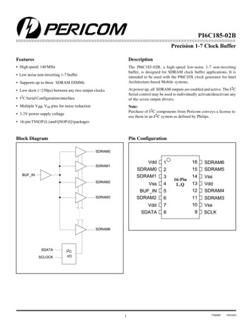
4567890123456789012123456789012Precision 1-7 Clock BufferFeaturesDescription High speed: 140 MHzThe PI6C185-02B, a high-speed low-noise 1-7 non-invertingbuffer, is designed for SDRAM clock buffer applications. It isintended to be used with the PI6C10X clock generator for IntelArchitecture-based Mobile systems. Low noise non-inverting 1-7 buffer Supports up to three SDRAM DIMMsAt power up, all SDRAM outputs are enabled and active. The I2CSerial control may be used to individually activate/deactivate anyof the seven output drivers. Low skew ( 250ps) between any two output clocks I2C Serial Configuration interface Multiple Vdd, Vss pins for noise reductionNote:Purchase of I2C components from Pericom conveys a license touse them in an I2C system as defined by Philips. 3.3V power supply voltage 16-pin TSSOP (L) and QSOP (Q) packagesBlock DiagramPin ConfigurationSDRAM0VddSDRAM0SDRAM1VssBUF INSDRAM2VddSDATASDRAM1BUF INSDRAM2. . . . . . PS846905/03/00
PI6C185-02BPrecision 1-7 Clock 1212345678901234567890123456789012123456789012Pin DescriptionPinSignalTypeQty.D e s cription2,3,6,11,12,15,16SDRAM [0.6]I7Buffered Clock O utputs5BUF INI1Clock Buffer Input8SDATAI/O1Serial Data for I2C interface9SCLKI1Serial Clock for I2C interface1,7,13VDDPower33.3V Power Supply4,10,14VSSGround3GroundPI6C185-02B I2C Address AssignmentA6A5A4A3A2A1A0R/W11010010PI6C185-02 Serial Configuration MapByte1: SDRAM Active/Inactive Register(1 enable, 0 disable)Byte0: SDRAM Active/Inactive Register(1 enable, 0 disable)BitPin #Bit 76Bit 6D e s criptionBitPin#D e s criptionSDRAM2Bit 716SDRAM6-NC (Initialize to 0)Bit 615SDRAM5Bit 5-NC (Initialize to 0)Bit 5-NC (Initialize to 0)Bit 4-NC (Initialize to 0)Bit 4-NC (Initialize to 0)Bit 33SDRAM1Bit 312SDRAM4Bit 22SDRAM0Bit 211SDRAM3Bit 1-NC (Initialize to 0)Bit 1-NC (Initialize to 0)Bit 0-NC (Initialize to 0)Bit 0-NC (Initialize to 0)Note: Inactive means outputs are held LOWand are disabledfrom switching2PS846905/03/00
PI6C185-02BPrecision 1-7 Clock 9012345678901234567890121234567890122-Wire I2C ControlThe I2C interface permits individual enable/disable of each clockoutput and test mode enable.Each data transfer is initiated with a start condition and ended witha stop condition. The first byte after a start condition is always a7-bit address byte followed by a read/write bit. (HIGH read fromaddressed device, LOW write to addressed device). If the device’sown address is detected, PI6C185-02B generates an acknowledgeby pulling SDATA line LOW during ninth clock pulse, thenaccepts the following data bytes until another start or stop conditionis detected.The PI6C185-02B, a slave receiver device, cannot be read back.Sub addressing is not supported. To change one of the controlbytes, all preceding bytes must be sent.Every byte put on the SDATA line must be 8-bits long (MSB first),followed by an acknowledge bit generated by the receivingdevice.123Following acknowledgement of the address byte (0D2H), two morebytes must be sent:During normal data transfers, SDATA changes only when SCLK isLOW. Exceptions: A HIGH to LOW transition on SDATA whileSCLK is HIGH indicates a “start” condition; a LOW to HIGHtransition on SDATA while SCLK is HIGH is a “stop” conditionand indicates the end of a data transfer cycle.41. “Command Code” byte &2. “Byte Count” byte.Although the data bits on these two bytes are “don’t care,” theymust be sent and acknowledged.5Maximum Ratings(Above which the useful life may be impaired. For user guidelines, not tested.)Note:Storage Temperature . –65 C to 150 C Stresses greater than those listed under MAXIMUM RATINGSAmbient Temperature with Power Applied . –0 C to 70 C may cause permanent damage to the device. This is a stress ratingonly and functional operation of the device at these or any other3.3V Supply Voltage to Ground Potential . –0.5V to 4.6Vconditions above those indicated in the operational sections ofDC Input Voltage . –0.5V to 4.6V this specification is not implied. Exposure to absolute maximumrating conditions for extended periods may affect reliability.678Supply Current (VDD 3.465V, Cload max)SymbolParame te rTe s t ConditionIDDSupply CurrentBUF IN 0 MHzIDDSupply CurrentBUF IN 66.66 MHzIDDSupply CurrentBUF IN 100.0 MHzM in.Typ.M ax.9Units3TBD10mA1112131415PS8469305/03/00
PI6C185-02BPrecision 1-7 Clock 1212345678901234567890123456789012123456789012DC Operating Specifications (VDD 3.3V 5%, TA 0 C –70 C)SymbolParame te rConditionM in.M ax.UnitsVDD2.0VDD 0.3VSS 0.30.80 VIN VDD-5 52.4Input VoltageVIHInput High VoltageVILInput Low VoltageIILInput Leakage CurrentVµAVDD 3.3V 5%VOHOutput High VoltageIOH 1mAVOLOutput Low VoltageIOL 1mACINInput Pin Capacitance5COUTOutput pins Capacitance6LPINPin Inductance7nH70ºCTAAmbient TemperatureV0.4No Airflow0pFSDRAM Clock Buffer Operating SpecificationSymbolParame te rConditionM in. Typ. M ax. UnitsIOHMINPull- up currentVOUT 2.0VIOHMAXPull- up currentVOUT 3.135VIOLMINPull- down currentVOUT 1.0VIOLMAXPull- down currentVOUT 0.4VtRHSDRAMOutput rise edge rateSDRAM only3.3V 5%@0.4V- 2.4V1.54tFHSDRAMOutput fall edge rateSDRAM only3.3V 5%@2.4V- 0.4V1.54 4036mA4038V/nsAC TimingSymbolParame te r66 M Hz100 M Hz133 M HzM in.M ax.M in.M ax.M in.M ax.15.510.010.57.57.8UnitstSDKPSDRAM CLK period15.0tSDKHSDRAM CLK high time5.63.31.0tSDKLSDRAM CLK low time5.33.11.0tSDRISESDRAM CLK rise time1.54.01.54.01.54.0tSDFALLSDRAM CLK fall time1.54.01.54.01.54.0tPLHSDRAM Buffer LH prop delay1.05.51.05.51.05.5tPHLSDRAM Buffer HL prop delay1.05.51.05.51.05.5tPZL,tPZHSDRAM Buffer Enable delay1.08.01.08.01.08.0tPLZ,tPHZSDRAM Buffer Disable delay1.08.01.08.01.08.0Duty CycleMeasured at 1.5V455545554555%tSDSKWSDRAM Output to Output Skew250ps2502504nsV/nsnsPS846905/03/00
PI6C185-02BPrecision 1-7 Clock ntBuffer2Test lhOutput1.5VWaveform81.5V9Figure 1. Clock Waveforms10Minimum and Maximum Expected Capacitive LoadsClockSDRAMM in Load M ax Load1520UnitspFNote sSDRAM DIMM Specification11Notes:1. Maximum rise/fall times are guaranteed at maximum specified load.2. Minimum rise/fall times are guaranteed at minimum specified load.3. Rise/fall times are specified with pure capacitive load as shown.Testing is done with an additional 500Ω resistor in parallel.1213Design Guidelines to Reduce EMI141. Place RS series resistors and CI capacitors as close as possible to the respective clock pins. Typicalvalue for CI is 10pF. RS Series resistor value can be increased to reduce EMI provided that the riseand fall time are still within the specified values.2. Minimize the number of “vias” of the clock traces.3. Route clock traces over a continuous ground plane or over a continuous power plane. Avoid routingclock traces from plane to plane (refer to rule #2).4. Position clock signals away from signals that go to any cables or any external connectors.15PS8469505/03/00
PI6C185-02BPrecision 1-7 Clock 185-02B100/66 MHzClock fromChipsetSDRAMRS7CLSDRAMDIMMSpec.Figure 2. Design Guidelines16-Pin TSSOP (L) Package16-Pin QSOP (Q) Package1616.150.157.169.1773.813.994.34.5.015 x 45 5.007.012.002.0060.090.200.45 .0180.75 40.41 .0161.27 .050.0080.203 REF.252BSC6.4.228.2445.796.19.053 1.35.069 120.2030.305.004 0.101.010 0.254X.XX DENOTES CONTROLLINGX.XX DIMENSIONS IN MILLIMETERSX.XX DENOTES DIMENSIONSX.XX IN MILLIMETERSOrdering InformationP/ND e s criptionPI6C185- 02BLTSSO P PackagePI6C185- 02BQQ SO P PackagePericom Semiconductor Corporation2380 Bering Drive San Jose, CA 95131 1-800-435-2336 Fax (408) 435-1100 http://www.pericom.com6PS846905/03/00
Ł I2C Serial Configuration interface Ł Multiple Vdd, Vss pins for noise reduction Ł 3.3V power supply voltage Ł 16-pin TSSOP (L) and QSOP (Q) packages Description The PI6C185-02B, a high-speed low-noise 1-7 non-inverting buffer, is designed for SDRAM clock buffer applications. It is intended to be used with the PI6C10X clock generator for Intel