Transcription
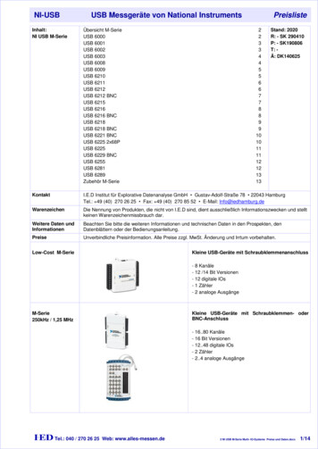
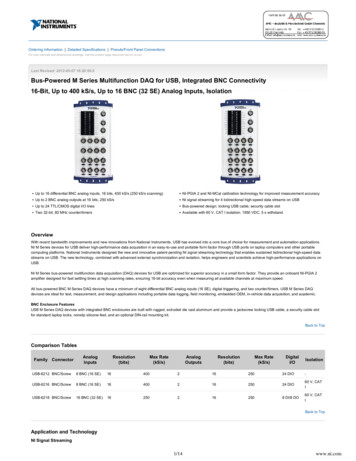
ProductFolderSample &BuySupport &CommunityTools SLLSE67I – MARCH 2011 – REVISED MARCH 2016TUSB9261 USB 3.0 to SATA Bridge1 Features2 Applications The TUSB9261 is an ARM Cortex M3microcontroller based USB 3.0 to serial ATA bridge. Itprovides the necessary hardware and firmware toimplement a USB attached SCSI protocol (UASP)compliant mass storage device suitable for bridginghard disk drives (HDD), solid state disk drives (SSD),optical drives, and other compatible SATA 1.5-Gbpsor SATA 3.0-Gbps devices to a USB 3.0 bus. Inaddition to UASP support, the firmware implementsthe mass storage class BOT and USB HID interfaces.Device Information(1)PART NUMBERTUSB9261PACKAGEBODY SIZE (NOM)HTQFP (64)7.00 7.00 mm(1) For all available packages, see the orderable addendum atthe end of the data sheet.Simplified SchematicROMGRSTzARMCortex M3VDD3.3RAM64 kBVDD1.1TCKTMSTDOTDITRSTJTAGData PathRAM80 kBXIClockGenerationPowerandResetDistributionUSB DMUSB R1USB HS/FSPHYVBUSSSTX SSTX-USB SSPHYSSRX SSRX-SATATX SATATX-SATA IIPHYSATARX SATARX-CS[2:0]SCLKDATA INPWM[1:0]GPIOPWMSPIGPIO[11:0]SCI(UART)USB R1RTN 3 DescriptionDATA OUT External HDD/SSDExternal DVDExternal CDHDD-Based Portable Media PlayerUartTX Universal Serial Bus (USB)– SuperSpeed USB 3.0 Compliant – TID340730020– Integrated Transceiver Supports SS/HS/FSSignaling– Best-in-Class Adaptive Equalizer– Allows for Greater Jitter Tolerance in theReceiver– USB Class Support– USB Attached SCSI Protocol (UASP)– USB Mass Storage Class Bulk-OnlyTransport (BOT)– Support for Error Conditions Per the 13Cases (Defined in the BOT Specification)– USB Bootability Support– USB Human Interface Device (HID)– Supports Firmware Update Via USB, Using aTI Provided ApplicationSATA Interface– Serial ATA Specification Revision 2.6– Gen1i, Gen1m, Gen2i, and Gen2m– Support for Mass-Storage Devices CompatibleWith the ATA/ATAPI-8 SpecificationIntegrated ARM Cortex M3 Core– Customizable Application Code Loaded fromEEPROM by SPI Interface– Two Additional SPI Port Chip Selects forPeripheral Connection– Up to 12 GPIOs for End-User Configuration– Two GPIOs have PWM Functionality forLED Blink Speed Control– Serial Communications Interface for Debug(UART)General Features– Integrated Spread Spectrum Clock GenerationEnables Operation from a Single Low-CostCrystal or Clock Oscillator– Supports 40 MHz– A JTAG Interface is Used for IEEE1149.1 andIEEE1149.6 Boundary Scan– Available in a Fully RoHS-Compliant PackageUartRX11An IMPORTANT NOTICE at the end of this data sheet addresses availability, warranty, changes, use in safety-critical applications,intellectual property matters and other important disclaimers. PRODUCTION DATA.
TUSB9261SLLSE67I – MARCH 2011 – REVISED MARCH 2016www.ti.comTable of Contents1234567Features .Applications .Description .Revision History.Pin Configuration and Functions 77788899Absolute Maximum Ratings .ESD Ratings.Recommended Operating Conditions.Thermal Information .DC Electrical Characteristics for 3.3-V Digital I/O.SuperSpeed USB Power Consumption .High-Speed USB Power Consumption .Oscillator Specification.Crystal Specification.Detailed Description . 107.1 Overview . 107.2 Functional Block Diagram . 107.3 Feature Description. 107.4 Device Functional Modes. 138Application and Implementation . 158.1 Application Information. 158.2 Typical Application . 159Power Supply Recommendations. 199.1 Digital Supplies 1.1-V and 3.3-V . 199.2 Analog Supplies 1.1-V and 3.3-V . 1910 Layout. 1910.1 Layout Guidelines . 1910.2 Layout Examples. 2011 Device and Documentation Support . 2211.111.211.311.4Community Resources.Trademarks .Electrostatic Discharge Caution .Glossary .2222222212 Mechanical, Packaging, and OrderableInformation . 224 Revision HistoryNOTE: Page numbers for previous revisions may differ from page numbers in the current version.Changes from Revision H (July 2015) to Revision I PageChanged the CDM value in the ESD Ratings table From: 5000 To: 1500 . 7Changes from Revision G (October 2014) to Revision HPage Moved Tstg from Handling Ratings table to Absolute Maximum Ratings and renamed Handling Ratings to ESD Ratings . 7 Updated the frequency for the USB2 and USB3 to 5 Hz and 10 Hz, respectively . 16Changes from Revision F (March 2014) to Revision GPage Updated supported frequency to 40 MHz . 1 Updated supported frequency in Clock and Reset Signals table . 4 Updated the frequency for the clock to 40 MHz . 9 Updated the frequency for the crystal to 40 MHz . 9 Updated oscillation frequency and ESR equivalent series resistance . 9 Updated Table 1 . 122Submit Documentation FeedbackCopyright 2011–2016, Texas Instruments IncorporatedProduct Folder Links: TUSB9261
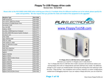
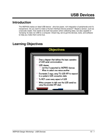
TUSB9261www.ti.comSLLSE67I – MARCH 2011 – REVISED MARCH 20165 Pin Configuration and FunctionsPVP Package48-Pin HTQFPTop ViewVDDVDDA33USB DMUSB DPNCUSB R1USB R1RTNVDDA33VDDUSB SSTXMUSB SSTXPVSSUSB SSRXMUSB SSRXPVDDVDDA3348 47 46 45 44 43 42 41 40 39 38 37 36 35 34 33VDDUSB VBUSVDD33XIVSSOSCXOVDDSATA TXMSATA TXPVSSSATA RXMSATA QSEL0JTAG TRSTzJTAG TMSJTAG TDOJTAG TDIJTAG TCKVDD33SPI CS2 / GPIO11SPI CS1 / GPIO10SPI CS0SPI DATA INVDDSPI DATA OUTSPI SCLK1 2 3 4 5 6 7 8 9 10 11 12 13 14 15 GPIO9 / UART TXGPIO8 / UART RXGRSTzPWM1PWM0VDDSubmit Documentation FeedbackCopyright 2011–2016, Texas Instruments IncorporatedProduct Folder Links: TUSB92613
TUSB9261SLLSE67I – MARCH 2011 – REVISED MARCH 2016www.ti.comSignal Descriptions – I/O DefinitionsI/O nal pullup resistorPDInternal pulldown resistorPWRPower signalClock and Reset al input. This terminal is the crystal input for the internal oscillator. The input may alternatelybe driven by the output of an external oscillator. When using a crystal, a 1-MΩ feedback resistoris required between X1 and XO.XO54OCrystal output. This terminal is the crystal output for the internal oscillator. If XI is driven by anexternal oscillator, this pin may be left unconnected. When using a crystal, a 1-MΩ feedbackresistor is required between X1 and XO.31, 30IPUFREQSEL[1:0]Global power reset. This reset brings all of the TUSB9261 internal registers to their defaultstates. When GRSTz is asserted, the device is completely nonfunctional.Frequency select. These terminals indicate the oscillator input frequency and are used toconfigure the correct PLL multiplier. The field encoding is as follows:FREQSEL[1]FREQSEL[0]INPUT CLOCK FREQUENCY1140 MHzSATA Interface Signals (1)PINNAMENO.I/ODESCRIPTIONSATA TXP57OSerial ATA transmitter differential pair (positive)SATA TXM56OSerial ATA transmitter differential pair (negative)SATA RXP60ISerial ATA receiver differential pair (positive)SATA RXM59ISerial ATA receiver differential pair (negative)(1)Note that the default firmware and reference design for the TUSB9261 have the SATA TXP/TXM swapped for ease of routing in thereference design. If you plan to use the TI default firmware please review the reference design in the TUSB9261 DEMO User’s Guide(SLLU139) for proper SATA connection.USB Interface SignalsPINNAMENO.I/ODESCRIPTIONUSB SSTXP43OSuperSpeed USB transmitter differential pair (positive)USB SSTXM42OSuperSpeed USB transmitter differential pair (negative)USB SSRXP46ISuperSpeed USB receiver differential pair (positive)USB SSRXM45ISuperSpeed USB receiver differential pair (negative)USB DP36I/OUSB high-speed differential transceiver (positive)USB DM35I/OUSB high-speed differential transceiver (negative)USB VBUS50IUSB bus powerUSB R138OPrecision resistor reference. A 10-kΩ 1% resistor should be connected between R1 and R1RTN.USB R1RTN39IPrecision resistor reference return4Submit Documentation FeedbackCopyright 2011–2016, Texas Instruments IncorporatedProduct Folder Links: TUSB9261
TUSB9261www.ti.comSLLSE67I – MARCH 2011 – REVISED MARCH 2016Serial Peripheral Interface (SPI) SignalsPINNAMENO.I/ODESCRIPTIONSPI SCLK17OPUSPI clockSPI DATA OUT18OPUSPI master data outSPI DATA IN20IPUSPI master data inSPI CS021OPUPrimary SPI chip select for flash RAM23I/OPUSPI chip select for additional peripherals. When not used for SPI chip select, this pin may be usedas a general-purpose I/O.22I/OPUSPI chip select for additional peripherals. When not used for SPI chip select, this pin may be usedas a general-purpose I/O.SPI CS2/GPIO11SPI CS1/GPIO10JTAG, GPIO, and PWM SignalsPINNAMENO.I/ODESCRIPTIONJTAG TCK25IPDJTAG test clockJTAG TDI26IPUJTAG test data inJTAG TDO27OPDJTAG test data outJTAG TMS28IPUJTAG test mode selectJTAG TRSTz29IPDJTAG test resetGPIO9/UART TX6I/OPUGPIO/UART transmitter. This terminal can be configured as a GPIO or as the transmitter for aUART channel. This pin defaults to a general-purpose output.GPIO8/UART RX5I/OPUGPIO/UART receiver. This terminal can be configured as a GPIO or as the receiver for a UARTchannel. This pin defaults to a general-purpose DPWM02OPD (1)PWM13OPD (1)(1)Configurable as general-purpose input/outputsPulse-width modulation (PWM). Can be used to drive status LEDs.PWM pulldown resistors are disabled by default. A firmware modification is required to turn them on. All other internal pull up/downresistors are enabled by default.Submit Documentation FeedbackCopyright 2011–2016, Texas Instruments IncorporatedProduct Folder Links: TUSB92615
TUSB9261SLLSE67I – MARCH 2011 – REVISED MARCH 2016www.ti.comPower and Ground 1-V power railPWR3.3-V power railPWR3.3-V analog power railPWROscillator ground. If using a crystal, this should not be connected to a PCB ground plane. Ifusing an oscillator, this should be connected to PCB ground. See Clock Source Requirementsfor more details.PWRGroundPWRGround – Thermal C6534458653764—No connect, leave floatingSubmit Documentation FeedbackCopyright 2011–2016, Texas Instruments IncorporatedProduct Folder Links: TUSB9261
TUSB9261www.ti.comSLLSE67I – MARCH 2011 – REVISED MARCH 20166 Specifications6.1 Absolute Maximum Ratingsover operating free-air temperature (unless otherwise noted)MINMAXUNITVDDSteady-state supply voltage–0.31.4VVDD33/VDDA33Steady-state supply voltage–0.33.8VTstgStorage temperature–55150 C6.2 ESD RatingsVALUEVESD(1)(2)Electrostatic dischargeHuman body model (HBM), per ANSI/ESDA/JEDEC JS001(1)UNIT 2000Charged device model (CDM), per JESD22-C101 (2)V 1500JEDEC document JEP155 states that 500-V HBM allows safe manufacturing with a standard ESD control process.JEDEC document JEP157 states that 250-V CDM allows safe manufacturing with a standard ESD control process.6.3 Recommended Operating Conditionsover operating free-air temperature range (unless otherwise noted)MINNOMMAXUNITVDDDigital 1.1-V supply voltage1.0451.11.155VVDD33Digital 3.3-V supply voltage33.33.6VVDDA33Analog 3.3-V supply voltage33.33.6VVBUSVoltage at VBUS PAD01.155V070–4085–40100TAOperating free-air temperature rangeTJOperating junction temperature rangeIndustrial version C C6.4 Thermal InformationTUSB9261THERMAL METRIC (1)PVP (HTQFP)UNIT64 PINSRθJAJunction-to-ambient thermal resistance30.2 C/WRθJC(top)Junction-to-case (top) thermal resistance11.0 C/WRθJBJunction-to-board thermal resistance6.1 C/WψJTJunction-to-top characterization parameter0.4 C/WψJBJunction-to-board characterization parameter6.1 C/WRJθC(bot)Junction-to-case (bottom) thermal resistance0.9 C/W(1)For more information about traditional and new thermal metrics, see the Semiconductor and IC Package Thermal Metrics applicationreport, SPRA953.Submit Documentation FeedbackCopyright 2011–2016, Texas Instruments IncorporatedProduct Folder Links: TUSB92617
TUSB9261SLLSE67I – MARCH 2011 – REVISED MARCH 2016www.ti.com6.5 DC Electrical Characteristics for 3.3-V Digital I/Oover operating free-air temperature range (unless otherwise noted)PARAMETERTEST CONDITIONSMINTYPMAXUNITDRIVERTRRise time5 pF1.5TFFall time5 pF1.53IOLLow-level output currentVDD33 3.3 V, TJ 25 C6IOHHigh-level output currentVDD33 3.3 V, TJ 25 C–6VOLLow-level output voltageIOL 2 mAVOHHigh-level output voltageIOL –2 mAVOOutput voltagensnsmAmA0.42.4VV0VDD33VRECEIVERVIInput voltage0VDD33VVILLow-level input voltage00.8VVIHHigh-level input voltage2VhysInput hysteresistTInput transition time (TR and TF)IIInput currentVI 0 V to VDD33CIInput capacitanceVDD33 3.3 V, TJ 25 CV200mV0.38410ns5µApF6.6 SuperSpeed USB Power ConsumptionPOWER RAILTYPICAL ACTIVE CURRENT (mA) (1)TYPICAL SUSPEND CURRENT (mA) (2)VDD112911536528VDD33(1)(2)(3)(3)Transferring data by SS USB to a SSD SATA Gen II device. No SATA power management, U0 only.SATA Gen II SSD attached no active transfer. No SATA power management, U3 only.All 3.3-V power rails connected together.6.7 High-Speed USB Power Consumption(1)(2)(3)8POWER RAILTYPICAL ACTIVE CURRENT (mA) (1)TYPICAL SUSPEND CURRENT (mA) (2)VDD11172153VDD33 (3)5628Transferring data via HS USB to a SSD SATA Gen II device. No SATA power management.SATA Gen II SSD attached no active transfer. No SATA power management.All 3.3-V power rails connected together.Submit Documentation FeedbackCopyright 2011–2016, Texas Instruments IncorporatedProduct Folder Links: TUSB9261
TUSB9261www.ti.comSLLSE67I – MARCH 2011 – REVISED MARCH 20166.8 Oscillator SpecificationXI should be tied to the 1.8-V clock source and XO should be left floating. VSSOSC should be connected to the PCB groundplane. A 40-MHz clock can be used.PARAMETERTEST CONDITIONSMINTYPUNITXI input capacitanceVILLow-level input voltageVIHHigh-level input voltageTtosc iFrequency toleranceTdutyDuty cycleTR/TFRise/fall time20% to 80%6nsRJReference clockJTF (1 sigma) (1) (2)0.8psTJReference clockJTF (total p-p) (2) (3)25ps50psTp-p(1)(2)(3)(4)Reference clock jitterTJ 25 CMAXCXI0.414pF0.7V50ppm1.05Operational temperatureV–5045%(Absolute p-p)50%55%(4)Sigma value assuming Gaussian distributionAfter application of JTFCalculated as 14.1 RJ DJAbsolute phase jitter (p-p)6.9 Crystal SpecificationA parallel, 20-pF load capacitor should be used if a crystal source is used. VSSOSC should not be connected to the PCBground plane. A 40-MHz crystal can be used.PARAMETERTEST CONDITIONSMINOscillation modeTYPMAXUNITFundamentalƒOOscillation frequencyESREquivalent series resistance40 MHz40Ttosc iFrequency toleranceFrequency stabilityMHz50ΩOperational temperature 50ppm1 year aging 50ppm24pFCLLoad capacitanceCSHUNTCrystal and board stray capacitance12204.5pFDrive level (max)0.8mWSubmit Documentation FeedbackCopyright 2011–2016, Texas Instruments IncorporatedProduct Folder Links: TUSB92619
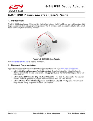
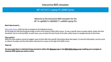
TUSB9261SLLSE67I – MARCH 2011 – REVISED MARCH 2016www.ti.com7 Detailed Description7.1 OverviewThe major functional blocks are as follows: Cortex M3 microcontroller subsystem including the following peripherals:– Time interrupt modules, including watchdog timer– Universal asynchronous receive/transmit (SCI)– SPI– General purpose input/output (GPIO)– PWM for support of PWM outputs (PWM) USB 3.0 core (endpoint controller) and integrated USB 3.0 PHY AHCI-compliant SATA controller and integrated SATA PHY– Supporting Gen1i, Gen1m, Gen2i, and Gen2m Chip level clock generation and distribution Support for JTAG 1149.1 and 1149.67.2 Functional Block DiagramUSB 3.0(1)SuperSpeedPCwithUSB 3.0SupportSATAGen1/2HDDUSB 2.0(1)High-speedTUSB9260TUSB9261A.USB connection is made at either SuperSpeed or high speed, depending on the upstream connection support.7.3 Feature Description7.3.1 Operation7.3.1.1 General FunctionalityThe TUSB9261 ROM contains boot code that executes after a global reset, which performs the initialconfiguration required to load a firmware image from an attached SPI flash memory to local RAM.After the firmware is loaded, it configures the SATA advanced host controller interface host bus adapter (AHCI)and the USB device controller. In addition, the configuration of the AHCI includes a port reset, which initiates anout of band (OOB) TX sequence from the AHCI link layer to determine if a device is connected, and if so,negotiate the connection speed with the device (3.0 Gbps or 1.5 Gbps).The configuration of the USB device controller includes creation of the descriptors, configuration of the deviceendpoints for support of UASP and USB mass storage class BOT, allocation of memory for the transmit requestblocks (TRBs), and creation of the TRBs necessary to transmit and receive packet data over the USB. Inaddition, the firmware provides any other custom configuration required for application-specific implementation,for example, a HID interface for user initiated backup.10Submit Documentation FeedbackCopyright 2011–2016, Texas Instruments IncorporatedProduct Folder Links: TUSB9261
TUSB9261www.ti.comSLLSE67I – MARCH 2011 – REVISED MARCH 2016Feature Description (continued)After the USB device controller configuration is complete, if a SATA device was detected during the AHCIconfiguration, the firmware connects the device to the USB bus when VBUS is detected. According to the USB3.0 specification, the TUSB9261 initially tries to connect at SuperSpeed USB. If successful, it enters U0;otherwise, after the training time out, it enables the DP pullup and connects as a USB 2.0 high-speed or fullspeed device depending on the speed supported by host or hub port.When connected, the firmware presents the BOT interface as the primary interface and the UASP interface asthe secondary interface. If the host stack is UASP aware, it can enable the UASP interface using aSET INTERFACE request for alternate interface 1.Following speed negotiation, the device should transmit a device to host (D2H) FIS with the device signature.This first D2H FIS is received by the link layer and copied to the port signature register. When firmware is notifiedof the device connection, it queries the device for capabilities using the IDENTIFY DEVICE command. Firmwarethen configures the device as appropriate for its interface and features supported, for example, an HDD thatsupports native command queuing (NCQ).7.3.1.2 Firmware SupportDefault firmware support is provided for the following: SuperSpeed USB and USB 2.0 high speed and full speed USB attached SCSI protocol (UASP) USB mass storage class (MSC) bulk-only transport (BOT)– Including the 13 error cases USB mass storage specification for bootability USB device class definition for HID– Firmware update and custom functionality (for example, one-touch backup) Serial ATA advanced host controller interface (AHCI) GPIO– LED control and custom functions (for example, one-touch backup control) PWM– LED dimming control SPI– Firmware storage and storing custom device descriptors Serial communications interface (SCI)– Debug output onlySubmit Documentation FeedbackCopyright 2011–2016, Texas Instruments IncorporatedProduct Folder Links: TUSB926111
TUSB9261SLLSE67I – MARCH 2011 – REVISED MARCH 2016www.ti.comFeature Description (continued)7.3.1.3 GPIO/PWM LED DesignationsThe default firmware provided by TI drives the GPIO and PWM outputs as listed in Table 1.Table 1. GPIO/PWM LED ned. Can use HID commands to change to output low or high.[internal 100-µA PD]InputGPIO1USB 3.0 Link State if U1/U2 enabled, otherwise [input with 100-µA PD]OutputGPIO5USB 3.0 Link State if U1/U2 enabled, otherwise [input with 100-µA PD]OutputU0: Off/OffU1: On/OffGPIO1/GPIO5USB3 power state (U0 to U3) U2: Off/OnOutputU3: On/OnOther: Off/OffGPIO2HS/FS suspendOutputGPIO3[INPUT with 100-µA PD] momentary push buttonInputGPIO4Bus- or self-powered indicator. (GPIO level should be HIGH when selfpowered). [internal 100-µA PD]InputGPIO6Undefined. Can use HID commands to change to output low or high.[internal 100-µA PD]InputGPIO7SS connectionOutputGPIO10Undefined. Can use HID commands to change to output low or high.Compile option to configure as SATA drive power enable output.[internal 100-µA PU]InputGPIO11Power fault indicator. [internal 100-µA PU]InputPWM0Disk activity (LED blink rate is faster when connected at USBSuperSpeed), USB connection (LED on), and USB suspend (fadingLED).OutputPWM1SW heartbeatOutputThe LEDs on the TUSB9261 product development kit (PDK) board are connected as in Table 1. See theTUSB9261 PDK Guide for more information on GPIO LED connection and usage. This EVM is available forpurchase. Contact TI for ordering information.7.3.1.4 Power-Up and Reset SequenceThe core power (VDD) must be present and at its minimum high level prior to, or at the same time that, the I/Opower (VDD33).In addition, meet the following constraints: All maximum ratings and recommended operating conditions are observed. All warnings about exposure to maximum rated and recommended conditions are observed, particularlyjunction temperature. These apply to power transitions as well as normal operation. Bus contention while VDD33 is powered up must be limited to 100 hours over the projected lifetime of thedevice. Bus contention while VDD33 is powered down may violate the absolute maximum ratings.A supply bus is powered up when the voltage is within the recommended operating range. It is powered downwhen it is below that range, either stable or in transition.A minimum reset duration of 2 ms is required. This is defined as the time when the power supplies are in therecommended operating range to the deassertion of GRSTz.12Submit Documentation FeedbackCopyright 2011–2016, Texas Instruments IncorporatedProduct Folder Links: TUSB9261
TUSB9261www.ti.comSLLSE67I – MARCH 2011 – REVISED MARCH 20167.3.2 Clock Connections7.3.2.1 Clock Source RequirementsThe TUSB9261 supports an external oscillator source or a crystal unit. If a clock is provided to XI instead of acrystal, XO is left open and VSSOSC should be connected to the PCB ground plane. Otherwise, if a crystal isused, the connection needs to follow these guidelines.Because XI and XO are coupled to other leads and supplies on the PCB, it is important to keep them as short aspossible and away from any switching leads. TI also recommends to minimize the capacitance between XI andXO. This can be accomplished by connecting the VSSOSC lead to the two external capacitors CL1 and CL2 andshielding them with the clean ground lines. The VSSOSC should not be connected to PCB ground when using acrystal.Load capacitance (Cload) of the crystal (varies with the crystal vendor) is the total capacitance value of the entireoscillation circuit system as seen from the crystal. It includes two external capacitors, CL1 and CL2, in Figure 1.The trace length between the decoupling capacitors and the corresponding power pins on the TUSB9261 mustbe minimized. TI also recommends that the trace length from the capacitor pad to the power or ground plane beminimized.CL1XIVSSOSCCrystalXOCL2Figure 1. Typical Crystal Connections7.3.2.2 Clock Source Selection GuideReference clock jitter is an important parameter. Jitter on the reference clock degrades both the transmit eye andreceiver jitter tolerance no matter how clean the rest of the PLL is, thereby impairing system performance.Additionally, a particularly jittery reference clock may interfere with the PLL lock detection mechanism, forcing thelock detector to issue an Unlock signal. A good-quality, low-jitter reference clock is required to achievecompliance with supported USB3.0 standards. For example, USB3.0 specification requires the random jitter (RJ)component of either RX or TX to be 2.42 ps (random phase jitter calculated after applying jitter transfer function(JTF)). As the PLL typically has a number of additional jitter components, the reference clock jitter must beconsiderably below the overall jitter budget.7.4 Device Functional Modes7.4.1 VBUS PowerPower can be supplied by a USB cable on the terminal VBUS. When using power from VBUS, both theTUSB9261 and the SATA device are allowed to draw only up to 500 mA from VBUS when operating.7.4.2 External PowerPower can be supplied from an external power source. When using an external power source, both theTUSB9261 and the SATA interface can draw all their current from the external supply.Submit Documentation FeedbackCopyright 2011–2016, Texas Instruments IncorporatedProduct Folder Links: TUSB926113
TUSB9261SLLSE67I – MARCH 2011 – REVISED MARCH 2016www.ti.comDevice Functional Modes (continued)7.4.3 External Voltage RegulatorBecause the TUSB9261 requires two voltage supplies (1.1 V and 3.3 V), TI recommends a multi-channel voltageregulator. The TPS650061 or TPS65024x are good choices. The TPS650061 uses a DC-DC converter and twoLDO regulators in a single package. The DC-DC converter can supply 1-A nominal current while the two LDOscan supply 300-mA nominal current. Because the 1.1-V supply can consume upwards of 340 mA of current, theDC-DC converter is ideal for supplying the 1.1-V current while the two LDOs can be used to supply 3.3-V current.Likewise the TPS65024x uses three DC-DC converters and three LDOs. Both devices also have a built-insupervisor circuit that can be connected to GRST on the TUSB9261.14Submit Documentation FeedbackCopyright 2011–2016, Texas Instruments IncorporatedProduct Folder Links: TUSB9261
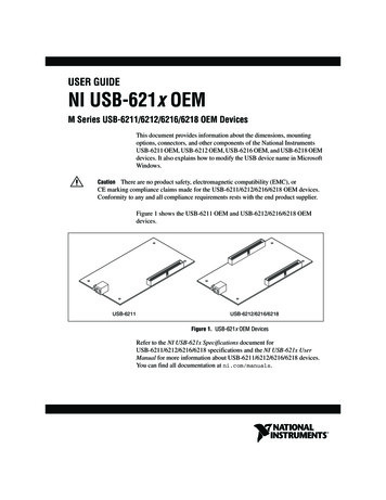
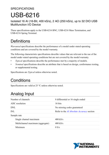
TUSB9261www.ti.comSLLSE67I – MARCH 2011 – REVISED MARCH 20168 Application and ImplementationNOTEInformation in the following applications sections is not part of the TI componentspecification, and TI does not warrant its accuracy or completeness. TI’s customers areresponsible for determining suitability of components for their purposes. Customers shouldvalidate and test their design implementation to confirm system functionality.8.1 Application InformationThe device serves as a bridge between a downstream USB 3.0 host port and a SATA device such as a hard diskdrive. A crystal or oscillator supplies the required clock source. A SPI flash device contains the firmware that isloaded into the TUSB9261 after the deassertion of RESET. Push buttons or any other desired logic can beconnected to the TUSB9261 GPIO pins. The TUSB9261 can also output a pulse-width modulated signal that canbe used to drive an activity LED.8.2 Typical AGUSB 3.0SuperSpeedSATAGen 1/2PC withUSB 3.0SupportSerial ATA DeviceUSB 2.0High-speedCLOCKGPIO/PWMHDDActivityLEDCrystal orOscillatorFigure 2. Typical Application Schematic8.2.1 Design RequirementsTable 2. Design ParametersDESIGN PARAMETEREXAMPLE VALUEVDD supply1.1 VVDD33 supply3.3 VUpstream port USB supportSS, HS, FSMain supplyVBUSUSB VBUS resistor values90.9 kΩ, 10 kΩCrystal frequency40 MHzSATA deviceSSDSubmit Documentation FeedbackCopyright 2011–2016, Texas Instruments IncorporatedProduct Folder Links: TUSB926115
TUSB9261SLLSE67I – MARCH 2011 – REVISED MARCH 2016www.ti.com8.2.2 Detailed Design Procedure8.2.2.1 PWM TerminalsThe TUSB9261 has two pulse-width modulated output terminals.Table 3 shows the default firmware configuration of PWMs.Table 3. Default Firmware Configuration of PWMsPWMUSAGE0Primary Indicator LED:ON when there is a USB connection. OFF when there is no connection.Blinks during disk activity (Frequency: 5 Hz for USB2 or 10 Hz for USB3).Fades when USB is in Suspend or U3 state.1Power indicator LEDPWM duty cycle will be 0% when the LED should be fully ON.8.2.2.2 JTAG InterfaceThe TUSB9261 supports JTAG for board-level test and debug support. Typically, these terminals are
1 Universal Serial Bus (USB) - SuperSpeed USB 3.0 Compliant - TID . - Serial ATA Specification Revision 2.6 - Gen1i, Gen1m, Gen2i, and Gen2m . implement a USB attached SCSI protocol (UASP)-compliant mass storage device suitable for bridging hard disk drives (HDD), solid state disk drives (SSD), .