Transcription
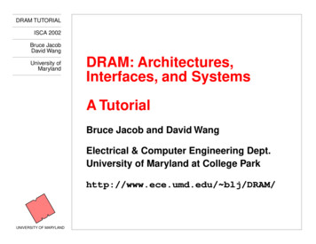
DRAM TUTORIALISCA 2002Bruce JacobDavid WangUniversity ofMarylandDRAM: why bother? (i mean,besides the “memory wall”thing? . is it just a performanceissue?)think about embedded systems:think cellphones, think printers,think switches . nearly everyembedded product that used tobe expensive is now cheap.why?for one thing, rapid turnover fromhigh performance toobsolescence guaranteesgenerous supply of CHEAP,HIGH-PERFORMANCEembedded processors to suitnearly any design need.what does the “memory wall”mean in this context? perhaps itwill take longer for a highperformance design to becomeobsolete?UNIVERSITY OF MARYLANDDRAM: Architectures,Interfaces, and SystemsA TutorialBruce Jacob and David WangElectrical & Computer Engineering Dept.University of Maryland at College Parkhttp://www.ece.umd.edu/ blj/DRAM/
DRAM TUTORIALISCA 2002OutlineBruce JacobDavid WangUniversity ofMaryland Basics DRAM Evolution: Structural Path Advanced Basics DRAM Evolution: Interface Path Future Interface Trends & Research Areas Performance Modeling:Architectures, Systems, EmbeddedNOTEBreak at 10 a.m. — Stop us or starve
DRAM TUTORIALISCA 2002BasicsBruce JacobDavid WangDRAM ORGANIZATIONDRAMfirst off -- what is DRAM? anarray of storage elements(capacitor-transistor pairs)Word LineSense AmpsData In/OutBuffers- capacitors are not perfect .need recharging- very dense parts; very small;capactiros have very littlecharge . thus, the bit lines arecharged up to 1/2 voltage leveland the ssense amps detect theminute change on the lines, thenrecover the full signalColumn Decoder. Bit Lines.Bit LineSwitchingelement. . Word Lines .“DRAM” is an acronym (explain)why “dynamic”?Storage element(capacitor)Row DecoderUniversity ofMarylandMemoryArray
DRAM TUTORIALISCA 2002BasicsBruce JacobDavid WangUniversity ofMarylandBUS TRANSMISSIONDRAMso how do you interact with thisthing? let’s look at a traditionalorganization first . CPUconnects to a memory controllerthat connects to the DRAM itself.Column Decoderlet’s look at a read operationSense AmpsData In/OutBuffers. . Word Lines . Bit Lines.Row DecoderCPUMEMORYBUS CONTROLLERMemoryArray
DRAM TUTORIALISCA 2002BasicsBruce JacobDavid WangUniversity ofMaryland[PRECHARGE and] ROW ACCESSDRAMat this point, all but lines are atttthe 1/2 voltage level.Column Decoderthe read discharges thecapacitors onto the bit lines .this pulls the lines just a little bithigh or a little bit low; the senseamps detect the change andrecover the full signalAKA: OPEN a DRAM Page/RoworACT (Activate a DRAM Page/Row)orRAS (Row Address Strobe). Bit Lines. . Word Lines .CPUMEMORYBUS CONTROLLERRow Decoderthe read is destructive -- thecapacitors have beendischarged . however, whenthe sense amps pull the lines tothe full logic-level (either high orlow), the transistors are keptopen and so allow their attachedcapacitors to become recharged(if they hold a ‘1’ value)Sense AmpsData In/OutBuffersMemoryArray
DRAM TUTORIALISCA 2002BasicsBruce JacobDavid WangUniversity ofMarylandCOLUMN ACCESSDRAMonce the data is valid on ALL ofthe bit lines, you can select asubset of the bits and send themto the output buffers . CASpicks one of the bitsSense AmpsData In/OutBuffersREAD CommandorCAS: Column Address Strobe. Bit Lines. . Word Lines .CPUMEMORYBUS CONTROLLERRow Decoderbig point: cannot do anotherRAS or precharge of the linesuntil finished reading the columndata . can’t change the valueson the bit lines or the output ofthe sense amps until it has beenread by the memory controllerColumn DecoderMemoryArray
DRAM TUTORIALISCA 2002BasicsBruce JacobDavid WangDATA TRANSFERDRAMthen the data is valid on the databus . depending on what youare using for in/out buffers, youmight be able to overlap a litttleor a lot of the data transfer withthe next CAS to the same page(this is PAGE MODE)Column DecoderSense AmpsData In/OutBuffersData Out. Bit Lines. . Word Lines .CPUMEMORYBUS CONTROLLERRow DecoderUniversity ofMarylandMemoryArray. with optional additionalCAS: Column Address Strobenote: page mode enables overlap with CAS
DRAM TUTORIALISCA 2002BasicsBruce JacobDavid WangUniversity ofMarylandBUS TRANSMISSIONDRAMNOTEColumn DecoderSense AmpsData In/OutBuffers. . Word Lines . Bit Lines.Row DecoderCPUMEMORYBUS CONTROLLERMemoryArray
DRAM TUTORIALISCA 2002BasicsBruce JacobDavid WangUniversity ofMarylandDRAM “latency” isn’tdeterministic because of CAS orRAS CAS, and there may besignificant queuing delays withinthe CPU and the memorycontrollerEach transaction has someoverhead. Some types ofoverhead cannot be pipelined.This means that in general,longer bursts are more efficient.FDRAMCPUMemE1ControllerABCDE2/E3A: Transaction request may be delayed in QueueB: Transaction request sent to Memory ControllerC: Transaction converted to Command Sequences(may be queued)D: Command/s Sent to DRAME1: Requires only a CAS orE2: Requires RAS CAS orE3: Requires PRE RAS CASF: Transaction sent back to CPU“DRAM Latency” A B C D E F
DRAM TUTORIALISCA 2002BasicsBruce JacobDavid WangPHYSICAL ORGANIZATIONNOTEMemoryArrayx2 DRAMx8 DRAMColumn DecoderSense AmpsDataBuffers. Bit Lines.MemoryArrayx4 DRAMThis is per bank Typical DRAMs have 2 banksColumn DecoderSense AmpsDataBuffers. Bit Lines. Bit Lines.x4 DRAM.Sense AmpsDataBuffersRow DecoderColumn DecoderRow Decoderx2 DRAMRow DecoderUniversity ofMarylandMemoryArrayx8 DRAM
DRAM TUTORIALISCA 2002BasicsBruce JacobDavid WangUniversity ofMarylandlet’s look at the interface anotherway . the say the data sheetsportray it.Read Timing for Conventional DRAMRASRow Access[explain]main point: the RAS\ and CAS\signals directly control thelatches that hold the row andcolumn addresses .Column AccessCASData ValidDataoutColumnAddressValidDataout
DRAM TUTORIALISCA 2002DRAM Evolutionary Tree.Bruce JacobDavid Wang.University ofMarylandMOSYSsince DRAM’s inception, therehave been a stream of changesto the design, from FPM to EDOto Burst EDO to SDRAM. thechanges are largely structuralmodifications -- nimor -- thattarget THROUGHPUT.[discuss FPM up to SDRAMEverything up to and includingSDRAM has been relativelyinexpensive, especially whenconsidering the pay-off (FPMwas essentially free, EDO cost alatch, PBEDO cost a counter,SDRAM cost a slight re-design).however, we’re run out of “free”ideas, and now all changes areconsidered expensive . thusthere is no consensus on newdirections and myriad of choiceshas appeared[ do LATENCY mods startingwith ESDRAM . and then theINTERFACE mods ]FCRAMConventionalDRAM (Mostly) Structural ModificationsTargeting cyEDOP/BEDOVCDRAMSDRAMESDRAMInterface ModificationsTargeting ThroughputRambus, DDR/2Future Trends
DRAM TUTORIALISCA 2002DRAM EvolutionBruce JacobDavid WangUniversity ofMarylandRead Timing for Conventional DRAMRow AccessNOTEColumn AccessTransfer OverlapData ddressValidDataoutColumnAddressValidDataout
DRAM TUTORIALISCA 2002DRAM EvolutionBruce JacobDavid WangUniversity ofMarylandRead Timing for Fast Page ModeRow AccessFPM aallows you to keep thesense amps actuve for multipleCAS commands .Column AccessTransfer Overlapmuch better throughputproblem: cannot latch a newvalue in the column addressbuffer until the read-out of thedata is completeData dDataout
DRAM TUTORIALISCA 2002DRAM EvolutionBruce JacobDavid WangUniversity ofMarylandRead Timing for Extended Data OutRow Accesssolution to that problem -instead of simple tri-statebuffers, use a latch as well.by putting a latch after thecolumn mux, the next columnaddress command can beginsoonerColumn AccessTransfer OverlapData dDataout
DRAM TUTORIALISCA 2002DRAM EvolutionBruce JacobDavid WangUniversity ofMarylandRead Timing for Burst EDORow Accessby driving the col-addr latch froman internal counter rather thanan external signal, the minimumcycle time for driving the outputbus was reduced by roughly30%Column AccessTransfer OverlapData dDataValidDataValidDataValidData
DRAM TUTORIALISCA 2002DRAM EvolutionBruce JacobDavid WangUniversity ofMarylandRead Timing for Pipeline Burst EDORow Access“pipeline” refers to the setting upof the read pipeline . first CAS\toggle latches the columnaddress, all following CAS\toggles drive data out onto thebus. therefore data stops comingwhen the memory controllerstops toggling CAS\Column AccessTransfer OverlapData dDataValidDataValidDataValidData
DRAM TUTORIALISCA 2002DRAM EvolutionBruce JacobDavid WangUniversity ofMarylandmain benefit: frees up the CPUor memory controller fromhaving to control the DRAM’sinternal latches directly . thecontroller/CPU can go off and doother things during the idlecycles instead of “wait” . eventhough the time-to-first-wordlatency actually gets worse, thescheme increases systemthroughputRead Timing for Synchronous DRAMRow AccessClockColumn AccessRASTransfer OverlapData lidDataValidDataValidDataValidData(RAS CAS OE . Command Bus)
DRAM TUTORIALISCA 2002DRAM EvolutionBruce JacobDavid WangUniversity ofMarylandoutput latch on EDO allowed youto start CAS sooner for nextaccesss (to same row)latch whole row in ESDRAM -allows you to start precharge &RAS sooner for thee next pageaccess -- HIDE THEPRECHARGE OVERHEAD.Inter-Row Read Timing for ESDRAMRegular CAS-2 SDRAM, R/R to same aValidDataValidDataESDRAM, R/R to same dDataValidDataValidData
DRAM TUTORIALISCA 2002DRAM EvolutionBruce JacobDavid WangUniversity ofMarylandneat feature of this type ofbuffering: write-aroundWrite-Around in ESDRAMRegular CAS-2 SDRAM, R/W/R to same bank, rows alidDataValidDataValidDataValidDataESDRAM, R/W/R to same bank, rows RowAddrColAddrColAddrValid ValidData idDataValid ValidData DataValid ValidData DataValid ValidData Data(can second READ be this aggressive?)ValidDataValidData
DRAM TUTORIALISCA 2002DRAM Evolution Bruce JacobDavid WangUniversity ofMarylandInternal Structure of Virtual Channel16 Channels(segments)Bank Bmain thing . it is like having abunch of open row buffers (a larambus), but the problem is thatyou must deal with the cachedirectly (move into and out of it),not the DRAM banks . adds anextra couple of cycles of latency. however, you get goodbandwidth if the data you want iscache, and you can “prefetch”into cache ahead of when youwant it . originally targetted atreducing latency, now thatSDRAM is CAS-2 and RCD-2,this make sense only in athroughput wayBank AInput/OutputBuffer2Kb Segment2Kb Segment2Kbit# DQsDQs2Kb Segment2Kb SegmentRow WriteSegment cache is software-managed, reduces energy
DRAM TUTORIALISCA 2002DRAM EvolutionBruce JacobDavid WangUniversity ofMarylandInternal Structure of Fast Cycle RAMSDRAMFCRAM13 bits8M Array(8Kr x 1Kb)Sense AmpstRCD 15ns(two clocks)15 bitsRow Decoder8K rows requires 13 bits ttoselect . FCRAM uses 15(assuming the array is 8k x 1k .the data sheet does not specify)Row DecoderFCRAM opts to break up thedata array . only activate aportion of the word line8M Array(?)Sense AmpstRCD 5ns(one clock)Reduces access time and energy/access
DRAM TUTORIALDRAM Evolution.ISCA 2002.Bruce JacobDavid WangUniversity ofMarylandMoSys takes this one stepfurther . DRAM with an SRAMinterface & speed but DRAMenergy[physical partitioning: 72 banks]Internal Structure of MoSys 1T-SRAMaddrBankSelectauto refresh -- how to do thistransparently? the logic movestthrough the arrays, refreshingthem when not active.but what is one bank getsrepeated access for a longduration? all other banks will berefreshed, but that one will not.solution: they have a bank-sizedCACHE of lines . in theory,should never have a problem(magic)AutoRefresh DQs
DRAM TUTORIALISCA 2002DRAM EvolutionBruce JacobDavid WangUniversity ofMarylandComparison of Low-Latency DRAM CoresDRAM TypeData BusSpeedBus Width(per chip)Peak BW(per Chip)RAS–CAS(tRCD)RAS–DQ(tRAC)PC133 SDRAM13316266 MB/s15 ns30 nsVCDRAM13316266 MB/s30 ns45 nsFCRAM200 * 216800 MB/s5 ns22 ns1T-SRAM20032800 MB/s—10 nsDDR 266133 * 216532 MB/s20 ns45 nsDRDRAM400 * 2161.6 GB/s22.5 ns60 nsRLDRAM300 * 2322.4 GB/s?25 nshere’s an idea of how thedesigns compare .bus speed CAS-to-CASRAS-CAS time to read datafrom capacitors into sense ampsRAS-DQ RAS to valid data
DRAM TUTORIALISCA 2002OutlineBruce JacobDavid WangUniversity ofMaryland Basics DRAM Evolution: Structural Path Advanced Basics Memory System Details (Lots) DRAM Evolution: Interface Path Future Interface Trends & Research Areas Performance Modeling:Architectures, Systems, Embedded
DRAM TUTORIALISCA 2002What Does This All Mean?Bruce JacobDavid WangSome Technology has legs,some do not have legs, andsome have gone belly up.We’ll start by emaining thefundamental technologies (I/Opackaging etc) then explore omeof these technologies in depth abit later.xDDR IInetDRAMEDOESDRAMFPMDDR IIRLDRAMBEDOSDRAMFCRAMD-RDRAMSLDRAMUniversity ofMarylandDDRSDRAM
DRAM TUTORIALISCA 2002Cost - Benefit CriterionB
DRAM TUTORIAL ISCA 2002 Bruce Jacob David Wang University of Maryland once the data is valid on ALL of the bit lines, you can select a subset of the bits and send them