Transcription
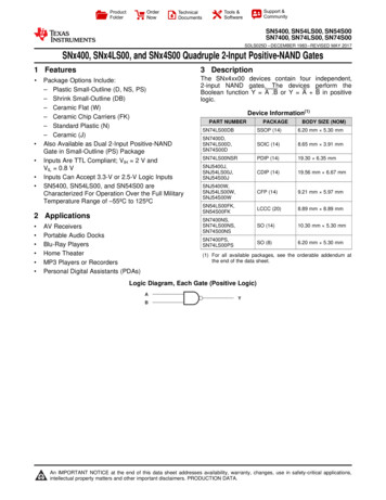
OrderNowProductFolderTechnicalDocumentsSupport &CommunityTools &SoftwareSN5400, SN54LS00, SN54S00SN7400, SN74LS00, SN74S00SDLS025D – DECEMBER 1983 – REVISED MAY 2017SNx400, SNx4LS00, and SNx4S00 Quadruple 2-Input Positive-NAND Gates1 Features3 Description The SNx4xx00 devices contain four independent,2-input NAND gates. The devices perform theBoolean function Y A .B or Y A B in positivelogic.1 Package Options Include:– Plastic Small-Outline (D, NS, PS)– Shrink Small-Outline (DB)– Ceramic Flat (W)– Ceramic Chip Carriers (FK)– Standard Plastic (N)– Ceramic (J)Also Available as Dual 2-Input Positive-NANDGate in Small-Outline (PS) PackageInputs Are TTL Compliant; VIH 2 V andVIL 0.8 VInputs Can Accept 3.3-V or 2.5-V Logic InputsSN5400, SN54LS00, and SN54S00 areCharacterized For Operation Over the Full MilitaryTemperature Range of –55ºC to 125ºC2 Applications AV ReceiversPortable Audio DocksBlu-Ray PlayersHome TheaterMP3 Players or RecordersPersonal Digital Assistants (PDAs)Device Information(1)PART NUMBERPACKAGEBODY SIZE (NOM)SN74LS00DBSSOP (14)6.20 mm 5.30 mmSN7400D,SN74LS00D,SN74S00DSOIC (14)8.65 mm 3.91 mmSN74LS00NSRPDIP (14)19.30 6.35 mmSNJ5400J,SNJ54LS00J,SNJ54S00JCDIP (14)19.56 mm 6.67 mmSNJ5400W,SNJ54LS00W,SNJ54S00WCFP (14)9.21 mm 5.97 mmSN54LS00FK,SN54S00FKLCCC (20)8.89 mm 8.89 mmSN7400NS,SN74LS00NS,SN74S00NSSO (14)10.30 mm 5.30 mmSN7400PS,SN74LS00PSSO (8)6.20 mm 5.30 mm(1) For all available packages, see the orderable addendum atthe end of the data sheet.Logic Diagram, Each Gate (Positive Logic)AYB1An IMPORTANT NOTICE at the end of this data sheet addresses availability, warranty, changes, use in safety-critical applications,intellectual property matters and other important disclaimers. PRODUCTION DATA.
SN5400, SN54LS00, SN54S00SN7400, SN74LS00, SN74S00SDLS025D – DECEMBER 1983 – REVISED MAY 2017www.ti.comTable of Contents1234567Features .Applications .Description .Revision History.Pin Configuration and Functions .106.1144466667778Absolute Maximum Ratings .ESD Ratings: SN74LS00 .Recommended Operating Conditions.Thermal Information .Electrical Characteristics: SNx400 .Electrical Characteristics: SNx4LS00 .Electrical Characteristics: SNx4S00 .Switching Characteristics: SNx400 .Switching Characteristics: SNx4LS00.Switching Characteristics: SNx4S00.Typical Characteristics .Parameter Measurement Information . 97.1 Propagation Delays, Setup and Hold Times, andPulse Width. 98Detailed Description . 108.1 Overview .8.2 Functional Block Diagram .8.3 Feature Description.8.4 Device Functional Modes.910101010Application and Implementation . 119.1 Application Information. 119.2 Typical Application . 1110 Power Supply Recommendations . 1211 Layout. 1311.1 Layout Guidelines . 1311.2 Layout Example . 1312 Device and Documentation Support . 1412.112.212.312.412.512.612.7Documentation Support .Related Links .Receiving Notification of Documentation UpdatesCommunity Resources.Trademarks .Electrostatic Discharge Caution .Glossary .1414141414141413 Mechanical, Packaging, and OrderableInformation . 154 Revision HistoryNOTE: Page numbers for previous revisions may differ from page numbers in the current version.Changes from Revision C (November 2016) to Revision D PageChanged Typical Application Diagram see Application and Implementation section. 1Changes from Revision B (October 2003) to Revision CPage Added ESD Ratings table, Feature Description section, Device Functional Modes, Application and ImplementationPower Supply Recommendations section, Layout section, Device and Documentation Support section, andMechanical, Packaging, and Orderable Information section. . 1 Changed Ordering Information table to Device Comparison Table; see Package Option Addendum at the end of thedata sheet . 1 Changed Package thermal impedance, RθJA, values in Thermal Information table From: 86 C/W To: 90.9 C/W (D),From: 96 C/W To: 102.8 C/W (DB), From: 80 C/W To: 54.8 C/W (N), and From: 76 C/W To: 89.7 C/W (NS). 62Submit Documentation FeedbackCopyright 1983–2017, Texas Instruments IncorporatedProduct Folder Links: SN5400 SN54LS00 SN54S00 SN7400 SN74LS00 SN74S00
SN5400, SN54LS00, SN54S00SN7400, SN74LS00, SN74S00www.ti.comSDLS025D – DECEMBER 1983 – REVISED MAY 20175 Pin Configuration and FunctionsSN5400 J, SN54xx00 J and W, SN74x00 D, N, and NS, orSN74LS00 D, DB, N, and NS Packages14-Pin CDIP, CFP, SOIC, PDIP, SO, or SSOPTop 83YSN74xx00 PS Package18-Pin SOTop ViewNot to scaleSN5400 W Package14-Pin CFPTop 83YNot to scale4B19Not to VCC420GND122A3Y6NC311YSN54xx00 FK Package20-Pin LCCCTop View112BNC71A221B10VCCGND81B131ANot to scalePin FunctionsPINCDIP, CFP, SOIC,PDIP, SO, 62B52Y63A3BNAMEI/ODESCRIPTIONIGate 1 input3IGate 1 input4OGate 1 output66IGate 2 input778IGate 2 input559OGate 2 output10—913IGate 3 input9—1014IGate 3 inputCopyright 1983–2017, Texas Instruments IncorporatedSubmit Documentation FeedbackProduct Folder Links: SN5400 SN54LS00 SN54S00 SN7400 SN74LS00 SN74S003
SN5400, SN54LS00, SN54S00SN7400, SN74LS00, SN74S00SDLS025D – DECEMBER 1983 – REVISED MAY 2017www.ti.comPin Functions (continued)PINCDIP, CFP, SOIC,PDIP, SO, 0)LCCC—812OGate 3 output—1218IGate 4 input12—1319IGate 4 input11—1416OGate 4 outputGND741110—GroundNC———1, 5, 7,11, 15, 17—No connectVCC148420—Power supplyNAME6 Specifications6.1 Absolute Maximum Ratingsover operating free-air temperature range (unless otherwise noted) (1)MINMAXUNIT7VSupply voltage, VCC (2)SNx400 and SNxS400Input voltage5.5SNx4LS00Junction temperature, TJStorage temperature, Tstg(1)(2)V7–65150 C150 CStresses beyond those listed under Absolute Maximum Ratings may cause permanent damage to the device. These are stress ratingsonly, which do not imply functional operation of the device at these or any other conditions beyond those indicated under RecommendedOperating Conditions. Exposure to absolute-maximum-rated conditions for extended periods may affect device reliability.Voltage values are with respect to network ground terminal.6.2 ESD Ratings: an-body model (HBM), per ANSI/ESDA/JEDEC JS-001 (1) 500Charged-device model (CDM), per JEDEC specification JESD22-C101 (2) 2000UNITVJEDEC document JEP155 states that 500-V HBM allows safe manufacturing with a standard ESD control process. Manufacturing withless than 500-V HBM is possible with the necessary precautions.JEDEC document JEP157 states that 250-V CDM allows safe manufacturing with a standard ESD control process. Manufacturing withless than 250-V CDM is possible with the necessary precautions. Pins listed as 2000 V may actually have higher performance. ESDTested on SN74LS00N package.6.3 Recommended Operating Conditionsover operating free-air temperature range (unless otherwise noted)VCCSupply voltageVIHHigh-level input voltageVILLow-level input voltageIOHHigh-level output currentIOLLow-level output N54LS000.7SN5400, SN54LS00, and SN74LS00Submit Documentation FeedbackUNITVVSNx400, SN7LS400, and SNx4S004MAXVmAmA20Copyright 1983–2017, Texas Instruments IncorporatedProduct Folder Links: SN5400 SN54LS00 SN54S00 SN7400 SN74LS00 SN74S00
SN5400, SN54LS00, SN54S00SN7400, SN74LS00, SN74S00www.ti.comSDLS025D – DECEMBER 1983 – REVISED MAY 2017Recommended Operating Conditions (continued)over operating free-air temperature range (unless otherwise noted)MINTAOperating free-air temperatureCopyright 1983–2017, Texas Instruments t Documentation FeedbackProduct Folder Links: SN5400 SN54LS00 SN54S00 SN7400 SN74LS00 SN74S00UNIT C5
SN5400, SN54LS00, SN54S00SN7400, SN74LS00, SN74S00SDLS025D – DECEMBER 1983 – REVISED MAY 2017www.ti.com6.4 Thermal InformationSN74LS00THERMAL METRIC (1) (2)RθJAD (SOIC)DB (SSOP)N (PDIP)NS (SO)14 PINS14 PINS14 PINS14 PINS90.9102.854.889.7 C/W51.953.342.148.1 C/W4853.434.850.1 C/WJunction-to-ambient thermal resistanceRθJC(top) Junction-to-case (top) thermal resistanceUNITRθJBJunction-to-board thermal resistanceψJTJunction-to-top characterization parameter18.616.526.916.7 C/WψJBJunction-to-board characterization parameter47.852.934.749.8 C/W(1)(2)For more information about traditional and new thermal metrics, see the Semiconductor and IC Package Thermal Metrics applicationreport.The package thermal impedance is calculated in accordance with JESD 51-7.6.5 Electrical Characteristics: SNx400over operating free-air temperature range (unless otherwise noted)PARAMETERTEST CONDITIONSMINTYPMAXUNIT–1.5VVIKVCC MIN and II –12 mAVOHVCC MIN, VIL 0.8 V, and IOH –0.4 mAVOLVCC MIN, VIH 2 V, and IOL 16 mAIIVCC MAX and VI 5.5 V1mAIIHVCC MAX and VI 2.4 V40µAIILVCC MAX and VI 0.4 V–1.6mAIOSVCC MAXICCHVCC MAX and VI 0 VICCLVCC MAX and VI 4.5 8mA1222mATYPMAXUNIT–1.5V6.6 Electrical Characteristics: SNx4LS00over operating free-air temperature range (unless otherwise noted)PARAMETERTEST CONDITIONSVIKVCC MIN and II –18 mAVOHVCC MIN, VIL MAX, and IOH –0.4 mAMIN2.53.4VIOL 4 mA0.250.4IOL 8 mA (SN74LS00)0.350.5VOLVCC MIN and VIH 2 VVIIVCC MAX and VI 7 V0.1mAIIHVCC MAX and VI 2.7 V20µAIILVCC MAX and VI 0.4 VIOSVCC MAXICCHVCC MAX and VI 0 VICCLVCC MAX and VI 4.5 V–0.4mA–100mA0.81.6mA2.44.4mA–206.7 Electrical Characteristics: SNx4S00over operating free-air temperature range (unless otherwise noted)PARAMETERTEST CONDITIONSMINTYPMAXUNIT–1.2VVIKVCC MIN and II –18 mAVOHVCC MIN, VIL 0.8 V, and IOH –1 mAVOLVCC MIN, VIH 2 V, and IOL 20 mAIIVCC MAX and VI 5.5 V1IIHVCC MAX and VI 2.7 V50µAIILVCC MAX and VI 0.5 V–2mA6Submit Documentation Feedback2.53.4V0.5VmACopyright 1983–2017, Texas Instruments IncorporatedProduct Folder Links: SN5400 SN54LS00 SN54S00 SN7400 SN74LS00 SN74S00
SN5400, SN54LS00, SN54S00SN7400, SN74LS00, SN74S00www.ti.comSDLS025D – DECEMBER 1983 – REVISED MAY 2017Electrical Characteristics: SNx4S00 (continued)over operating free-air temperature range (unless otherwise noted)PARAMETERTEST CONDITIONSMINTYP–40MAXUNITIOSVCC MAX–100mAICCHVCC MAX and VI 0 V1016mAICCLVCC MAX and VI 4.5 V2036mA6.8 Switching Characteristics: SNx400VCC 5 V, TA 25 C, and over operating free-air temperature range (unless otherwise noted). See Figure 2.PARAMETERtPLHFROM (INPUT)TO (OUTPUT)A or BtPHLYTEST CONDITIONSMINRL 400 Ω and CL 15 pFTYPMAX1122715TYPMAX9151015UNITns6.9 Switching Characteristics: SNx4LS00VCC 5 V, TA 25 C, and over operating free-air temperature range (unless otherwise noted). See Figure 2.PARAMETERtPLHtPHLFROM (INPUT)TO (OUTPUT)TEST CONDITIONSA or BYRL 2 kΩ and CL 15 pFMINUNITns6.10 Switching Characteristics: SNx4S00VCC 5 V, TA 25 C, and over operating free-air temperature range (unless otherwise noted). See Figure 2.PARAMETERtPLHtPHLFROM (INPUT)A or BA or BCopyright 1983–2017, Texas Instruments IncorporatedTO (OUTPUT)YYTYPMAXRL 280 Ω and CL 15 pFTEST CONDITIONSMIN34.5RL 280 Ω and CL 50 pF4.5RL 280 Ω and CL 15 pF3RL 280 Ω and CL 50 pF55Submit Documentation FeedbackProduct Folder Links: SN5400 SN54LS00 SN54S00 SN7400 SN74LS00 SN74S00UNITns7
SN5400, SN54LS00, SN54S00SN7400, SN74LS00, SN74S00SDLS025D – DECEMBER 1983 – REVISED MAY 2017www.ti.com6.11 Typical CharacteristicsCL 15 pFFigure 1. TPHL (Across Devices)8Submit Documentation FeedbackCopyright 1983–2017, Texas Instruments IncorporatedProduct Folder Links: SN5400 SN54LS00 SN54S00 SN7400 SN74LS00 SN74S00
SN5400, SN54LS00, SN54S00SN7400, SN74LS00, SN74S00www.ti.comSDLS025D – DECEMBER 1983 – REVISED MAY 20177 Parameter Measurement Information7.1 Propagation Delays, Setup and Hold Tim
An IMPORTANT NOTICE at the end of this data sheet addresses availability, warranty, changes, use in safety-critical applications, intellectual property matters and other important disclaimers. PRODUCTION DATA. SN5400, SN54LS00, SN54S00 SN7400, SN74LS00, SN74S00 SDLS025D –DECEMBER 1983–REVISED MAY 2017 SNx400, SNx4LS00, and SNx4S00 Quadruple 2-Input Positive-NAND