Transcription
IOP PUBLISHINGJOURNAL OF MICROMECHANICS AND . Micromech. Microeng. 21 (2011) 045022 (13pp)Vibration and shock reliability of MEMS:modeling and experimental validationSubramanian Sundaram1 , Maurizio Tormen2 , Branislav Timotijevic2 ,Robert Lockhart2 , Thomas Overstolz2 , Ross P Stanley2 andHerbert R Shea112Ecole Polytechnique Fédérale de Lausanne (EPFL), Neuchâtel 2002, SwitzerlandCentre Suisse d’Electronique et de Microtechnique, Neuchâtel 2002, SwitzerlandE-mail: herbert.shea@epfl.chReceived 20 December 2010, in final form 1 February 2011Published 17 March 2011Online at stacks.iop.org/JMM/21/045022AbstractA methodology to predict shock and vibration levels that could lead to the failure of MEMSdevices is reported as a function of vibration frequency and shock pulse duration. A combinedexperimental–analytical approach is developed, maintaining the simplicity and insightfulnessof analytical methods without compromising on the accuracy characteristic of experimentalmethods. The minimum frequency-dependent acceleration that will lead to surfaces cominginto contact, for vibration or shock inputs, is determined based on measured mode shapes,damping, resonant frequencies, and an analysis of failure modes, thus defining a safe operatingregion, without requiring shock or vibration testing. This critical acceleration for failure is astrong function of the drive voltage, and the safe operating region is predicted for transport(unbiased) and operation (biased condition). The model was experimentally validated forover-damped and under-damped modes of a comb-drive-driven silicon-on-insulator-basedtunable grating. In-plane and out-of-plane vibration (up to 65 g) and shock (up to 6000 g) testswere performed for biased and unbiased conditions, and very good agreement was foundbetween predicted and observed critical accelerations.(Some figures in this article are in colour only in the electronic version)Since MEMS differ from integrated circuits (ICs) inhaving μm-scale moving parts, much effort has been spenton understanding the mechanical reliability of MEMS: howdo MEMS fail under shock and vibration? Once that isunderstood, the question can be rephrased as: What is themaximum shock and vibration level that a MEMS device cansafely withstand? Importantly, how does the threshold evolveas a function of the drive voltage (for electrostatic MEMS)?This paper seeks to answer this question.Under shock and vibration, MEMS parts fail mainly by:(a) stiction when parts come into contact, (b) short-circuitor micro-welding when parts at different electrical potentialscome into contact, (c) fracture when a part is deformed to anextent such that the yield strength is exceeded, (d) short-circuitor mechanical blockage due to dust particles being moved, (e)fatigue for metal MEMS, (f) die-attach or package failure.Srikar and Senturia developed a useful classificationscheme to understand the reliability of MEMS in the presence1. IntroductionThe field of MEMS reliability is rapidly maturing: there arenow numerous examples of commercially available highlyreliable MEMS, and an increasingly mature understandingof MEMS-specific failure modes, design-for-reliabilitymethodologies, and improved characterization of the materialsused in MEMS [1, 2].In view of the large range of materials and actuationprinciples used in MEMS, general reliability guidelines canbe difficult to formulate. The electrical and mechanicalreliability of MEMS is reviewed in [1], to which the readeris referred to for a discussion of failure modes such asstiction [3], fatigue [4], fracture [5, 6], plastic deformation(creep) [7, 8], dielectric charging [9, 10], electrical breakdownand electrostatic discharge [11], radiation damage [12] andwear [5].0960-1317/11/045022 13 33.001 2011 IOP Publishing LtdPrinted in the UK & the USA
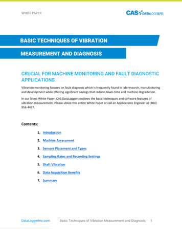
J. Micromech. Microeng. 21 (2011) 045022S Sundaram et alof mechanical shocks [13], showing the importance of theratio of shock pulse duration τ to the natural time period of thedevice Tvib . There have also been various attempts to studythe shock and vibration reliability of particular MEMSdevices at Sandia National Laboratories [14, 15] and at otherlaboratories [16]. These methods provide a qualitative insightinto the conditions that may cause failure but are not usefulfor making quantitative predictions, as they neither accountfor damping, nor for electrostatic spring softening. The failureconditions depend greatly on the actual design and dimensionsof the device. Therefore, results of shock or vibration tests witha particular device have little use in predicting the mechanicalreliability of a different device.Fully analytical approaches of modeling, though simpleand insightful, are not possible for complicated geometries.Moreover, it is difficult to incorporate fabrication tolerancesand inconsistencies in the material properties into the models.On the other hand, finite element method (FEM) solutionsrequire large computational resources and time for modelingand simulation of actual device geometries, and generally donot account well for the effect of the package.Even when using best practices, it can still be difficult todetermine, without lengthy experiments, the maximum safeshock and vibration levels for a MEMS component, and it isthus a challenge to design a part with the desired mechanicalreliability.To overcome some of these challenges, we present acombined experimental–analytical method to make qualitativeand quantitative predictions on the reliability of a generalMEMS device for shock and vibration inputs, retaining theadvantages of analytical methods without compromising onthe accuracy of the solution. This technique determines aconservative upper limit on the shock (peak acceleration andpulse duration) and vibration (amplitude versus frequency)that a MEMS device can repeatedly handle without failure. Inshort, the procedure involves three steps: (i) identifying all thecritical components in a device based on relative motions ofthe parts that can lead to failure, (ii) experimentally recordingeach part’s dynamic properties and (iii) using the analyticalmodel with these experimentally obtained parameters as inputsto predict the failure conditions, and hence a safe operatingenvelope. The procedure is summarized in figure 1 and isdescribed in detail in the following section.The methodology is presented in section 2. Analyticalmodels to predict failure due to shocks and vibrations aredescribed in section 3, based on measured device parameters(damping, resonant modes). A tunable grating made from asilicon-on-insulator (SOI) wafer is used to validate the resultsof this methodology. Shock and vibration tests (up to 6000and 65 g, respectively) were performed along the in-plane andout-of-plane directions. Details of the geometry of the device,working principle and characterization results are presented insection 4. Vibration and shock testing results as a functionof drive voltage are presented in section 5. Test results are ingood agreement with our theoretical predictions.Figure 1. Flowchart of the proposed methodology to obtain safeoperating conditions in the presence of shock and vibration inputs.(a)(b)Figure 2. Model of a single degree of freedom system for (a) forcedvibrations, (b) support excitation, which is the case we focus uponas it corresponds to applying shock or vibration to the package. Therelative displacement z x – y is the important value in this study.2. MethodologyThe objective is to determine a lower limit of mechanical shockand vibration that could lead to failure for a MEMS device.The first step (figure 1) is identifying possible mechanicalfailure modes and the associated required displacements forfailure. As a conservative approach, we choose contactbetween two parts as a failure criterion (e.g., if a proof masshits a stopper after moving 2 μm, this amplitude motion isdeemed a failure as it could potentially lead to stiction). Thisleads to an underestimate of the critical shock and vibration, asmechanical contact need not lead to stiction, especially whenthe parts are at the same potential. We shall return to thisin section 5. Fracture is also considered. For fracture, thetechnique does not lead to an underestimate; the uncertaintycomes from the Weibull distribution of fracture strengths.The second step is identifying the critical movingpart for each failure mechanism such as adjacent combfingers coming into contact, and approximating it as asingle degree of freedom (1DOF) system (see figure 2(a)).The equivalent parameters for the different 1DOFs, i.e. theresonant frequency and the damping coefficient, are obtainedexperimentally from the forced response of the system usingvarious experimental methods and tools such as a laserDoppler vibrometer (LDV), strobed microscopy, white light2
J. Micromech. Microeng. 21 (2011) 045022S Sundaram et alThe methodology described here can be used to predictresonant mode-related failures, i.e. where a failure is initiatedby a displacement resembling the resonant mode of thestructure. Under normal circumstances, specific resonantmodes are dominant over others. However, if two resonantmodes are equally dominant or if isolating the dominant modeis not simple, a single mode must be selected according to theinput conditions. For example, when devices are subjected toshocks, the mode that has a damped resonant frequency closeto the dominant frequency components present in the shock’sFourier spectrum must be considered. To identify vibrationrelated failures in such cases, the mode with a dampedresonant frequency close to the frequency of excitation ischosen as the dominant mode. Experimental characterizationtools like a LDV can also be used to definitively identifythe dominant modes. The competing modes can also beconsidered independently and the lowest estimate for thefailure criteria can be used as a conservative criterion forfailures.interferometry (WLI), capacitive sensing, LCR meter, etc.While the resonant frequencies are generally well known fromthe FEM, accurate damping coefficients must almost alwaysbe obtained experimentally. The device motion can be forcedin each mode electrostatically (generally the easiest method ifthe electrode configuration allows it), or with a small piezoshaker.The third step is using these parameters as inputsto analytically determine the shock and vibration levelsbelow which the failure mode cannot occur (either becauseparts will not come into contact or because critical strainsare not exceeded). These critical shock and vibrationlevels are generally a strong function of the appliedvoltage, and the model takes this into account, quicklyproviding, for instance, the maximum permissible shockduring transportation (unbiased) and during operation (biased).It has been difficult to date to efficiently and accuratelyincorporate all the damping mechanisms in simulations.Through the inclusion of measured damping properties in thisapproach, which is crucial as will be shown in the case study insection 5, our model is expected to have enhanced applicabilityand accuracy.Resonant frequencies and damping coefficients aregenerally easily obtainable using electrostatic excitation.Specially, no form of testing with vibration or shock inputsis required to predict the reliability. Additional effectssuch as those related to drive voltages (e.g., electrostaticspring softening or reduced gaps) can readily be incorporatedinto the model by making suitable changes to the inputparameters. Nonlinear effects, which are often importantin MEMS, can also be included.The method has abroad scope since it is developed for a general class ofMEMS and some possible applications are in tasks such asclassifying devices based on mechanical reliability, developingrobust structures, creating improved inertial MEMS, andoptimizing the operating voltages for improved reliability, anddetermining the maximum allowed in-use (biased), and storageor transportation (unbiased), vibrations and shocks.A 1DOF approximation (figure 2) has the advantage ofsimplicity, but has limitations if not used with care. Inthis work, we used a 1DOF transformation to convert themeasured experimental properties to the expected responsewhen subjected to external disturbances. The key to retainthe accuracy in spite of the reduced mathematical complexityis by carefully approximating the actual system. Here, weuse the 1DOF transformations at a single point, or at a rigidcomponent, and not for the entire system, i.e. we extractexperimental data at the most critical point in a device, fora particular failure mode. For instance, the LDV records thevelocities at a point where the laser strikes the device. Everysingle point in a structure, while it is excited in the resonantmode, can be effectively modeled as a 1DOF system withnegligible loss of accuracy. However, it is necessary to beaware that the constant parameter 1DOF system consideredhere can be used effectively only under a uniform rangeof excitation or displacements, i.e. the conditions duringcharacterization should be matched with the conditions wherethe extracted values are to be used. This will be discussed inlater sections.3. Modeling3.1. Vibration response modelA MEMS device experiences external vibrations and shocksas motion of the package. The MEMS component itself is notdirectly accelerated, and one must thus consider the relativemotion of the moving MEMS parts to the fixed parts. Forsimplicity, we shall not explicitly consider the effect of thepackage or of the support part of the chip. Figures 2(a) and (b)show the forced vibration model and the support excitationmodel of a 1DOF system where m is the effective massof the part, c is the effective damping coefficient, k is theeffective stiffness, F is the forcing function, x is the absolutedisplacement of the mass and y is the displacement of thesupport.The forced response of a 1DOF system with harmonicinput (see figure 2(a)) depends on the harmonic force F, thenatural frequency of the system ωn , the excitation frequencyω, and the damping ratio of the system ζ . The damping ratioζ can be expressed in terms of the damping coefficient c andthe quality factor Q as ζ c/(2mωn ) 1/(2Q).In the support vibration model, shown in figure 2(b), therelative displacement between the mass and the support isgiven as z x y. Vibrations that a package is subjectedto are felt as a periodic support excitation at the device end.The relative displacement of the part, z, due to the harmonicsupport excitation y can be written as 2 2 2 zωω 2ω 2ζ.(1)1 yωnωnωnThe amplitude of the frequency-dependent sinusoidalacceleration acrit required to bring parts into contact is thengiven by 2 2 ω 2ωcontact 2 ωn 2ζ(2) acrit amplitude z1 ωnωn3
J. Micromech. Microeng. 21 (2011) 045022S Sundaram et alspring softening for a linear parallel plate actuator, can bewritten as 2 Vd38ωres (V ) 1 (3)ωn27 (d x)3 Vpull inwhere d is the initial distance between the plates, x is thedisplacement of the mobile plate due to the application of avoltage V and Vpull in is the pull-in voltage.Two points are important to be carefully noted here.First, this equation can be directly applied only in the linearregime of the system, i.e. under conditions where the effectivespring constant does not depend on displacement amplitude.For large amplitude vibrations, the above equation has to bemodified to account for the nonlinear effects. A good accountof nonlinear effects in micro resonators is provided in [19].Secondly, it is preferable to use the above equation with thenatural undamped frequency of the system. If used with thedamped natural frequency, the obtained values may be largelydependent on the changes under the damping conditions. Oncethese two conditions are satisfied, this expression allows thedevice dynamics to be determined over a large voltage rangewith few experimental points. The damping coefficient is notexpected to change directly due to the spring softening, but canchange for instance if dominated by squeeze-film damping andif the applied bias changes a small gap in which the squeezefilm damping occurs.Figure 3. Computed critical acceleration for failure due to vibrationinputs, as a function of the excitation frequency, for three dampingconditions for a system with a resonant frequency of 2 kHz andassuming 1.6 μm motion leads to failure.where contactis the required displacement of the mass relativezto the support, for creating contact. The value of contactzis obtained after a careful analysis of all possible failuremechanisms and the geometries of the relevant parts, andwill be illustrated in sections 4 and 5 for several failuremodes of a tunable grating. The expression for the criticalacceleration given in (2) is the upper limit for the safe operatingconditions. The real value that causes failure is likely to behigher, especially for failures due to stiction, which requirea sufficient contact area for surface forces to overcome therestoring force of the spring.Figure 3 illustrates the critical conditions for vibrationinduced failure for a system with a 2 kHz resonant frequency,for damping ratios of 0.2, 1 and 1.75. The displacementrequired for failure is taken to be 1.6 μm. For excitations nearthe resonant frequency of the system, high damping helps tomake the device more robust.The above model is for a linear system. Nonlinearitiescan be important in MEMS, and the model must thereforebe adapted if the experimental data are taken only atsmall displacements. Ideally, all the parameters shouldbe extracted at the relevant displacements or the appliedvoltages, but this may often not be practical, as a mainobjective of this technique is to avoid high-g testing. Twomain nonlinear cases occur: for large displacements, thespring stiffness can increase. This is generally modeled asFspring k x k3 x3 . For example, in doubly clamped beams,nonlinear effects become relevant when the beam displacementis of the order of the beam thickness. The increasedspring constant leads to an increased resonant frequency andeventually to hysteretic behavior (Duffing curve) for largeramplitudes.For an electrostatic MEMS device, the effective springconstant decreases with increased voltage; this is theelectrostatic spring softening, as described in [17]. The moststriking example is the pull-in of parallel plate actuators,where the effective spring constant (and hence the resonancefrequency) drops to zero at snap-in [18]. For voltages below , due to apparentsnap-in the reduced resonant frequency ωres3.2. Shock response modelThe half-sine pulse waveform is used here to approximate theshocks experienced by devices, as it is one of the most commonshock waveforms [20] and provides an excellent descriptionof the acceleration curve that is observed in a pendulum shocktest, as discussed later. For a half-sine pulse, the two importantparameters are the peak acceleration amplitude ap and thepulse duration τ . The values of the pulse duration and thetime period of the system at resonance play an important role inthe shock reliability [13]. When the shock duration matchesthe time period of the system, the resonance modes of thesystem are excited and the effect of the shock is prominent.For a system with damping, as shown in figure 2(b),the equation of motion can be solved to obtain the relativedisplacement [21], which on further simplification becomes ÿz(t) L 1 ωn2 L 2s 2 2ζ ωn s ωn2(4)ωnwhere L[ ] and L 1 [ ] represent the Laplace and inverse Laplacetransformation operators, respectively, with s as the Laplacedomain variable.The half-sine pulse acceleration that the supportexperiences is written as a sin π t ; 0 t τpτÿ(t) .(5) 0;t τOn performing the Laplace transform of (5) and substitutingin (4), the relative displacement can now be written as R(t);0 t τz(t) (6)R(t) R(t τ ); t τ4
J. Micromech. Microeng. 21 (2011) 045022S Sundaram et al(a)(b)Figure 4. (a) Computed shock response of a 1DOF system with a resonant frequency of 2 kHz, plotted as the relative displacement of themass with respect to the support (corresponds to z in figure 2) versus time after the beginning of the shock pulse, for a peak shock amplitudeof 100 g and a pulse duration of 150 μs. (b) Plot of the computed critical acceleration for failure due to shock inputs, as a function of thehalf-sine pulse duration for a system with ωx 2 kHz with 1.6 μm displacement required for failure. Higher damping leads to a largercritical acceleration.where the coefficients η and λ are given by χ ωn (ζ ζ 2 1) δ ;η 2ωn ζ 2 1(12) χ ωn (ζ ζ 2 1) δ .λ 2ωn ζ 2 1Once the peak displacement is calculated from (6), using(9)–(11) depending on the damping conditions, the criticalacceleration causing the displacement required for failure iscomputed. The shock response, in terms of the displacementof the mass toward the support, obtained using (6) for a systemwith a resonant frequency of 2 kHz, when subjected to a100 g half-sine pulse shock with 150 μs duration is shownin figure 4 (a) for different damping ratios. The end of theshock pulse is indicated by a dotted vertical line. Based onthe peak displacements obtained from the above curve, thecritical conditions for shock inputs are obtained as a functionof the shock pulse duration for different damping ratios infigure 4(b). It can be seen that lower damping leads to lowercritical accelerations for shock-related failures. The curve forthe under-damped condition (ζ 0.2) has a local minimumwhen the shock pulse duration approaches the natural timeperiod of the system.and the complete solution of the relative displacement z(t)is known by solving for R(t) which is written in terms ofcoefficients α, β, χ and δ asR(t) apαs βπ 1χs δL 2222τs π /τs 2ζ ωn s ωn2where the coefficients are defined as qr pα ;β ;22(p r) pq(p r)2 pq 2qq2 r pχ ;δ ;22(p r) pq(p r)2 pq 2p π 2 /τ 2 ;q 2ζ ωn ;r ωn2 .(7)(8)Case (i). Under-damped system (ζ 1)R(t) in under-damped conditions is given by π βτ π πα cost sint e ζ ωn tR(t) apττπτ δ χ ζ ωn χ cos(ωdamped t) sin(ωdamped t) u(t)ωdamped(9)where u(t) is the step (Heaviside) function and ωdamped is thedamped natural frequency written as ωdamped ωn 1 ζ 2 .Case (ii). Critically damped system (ζ 1)For a critically damped system, R(t) is obtained as π π βτπR(t) apt sintα cosττπτ e ωn t .(χ (δ χ ωn )t) u(t).Case (iii). Over-damped system (ζ 1)For an over-damped system, R(t) is given by π π βτπt sintR(t) apα cosττπτ (ζ ζ 2 1)ωn t (ζ ζ 2 1)ωn t ηe λeu(t)4. Case study—electrostatically actuated MEMS:characterizationShock and vibration tests were performed on a tunablediffraction grating machined from an SOI wafer. The deviceswere initially characterized and the necessary parameters(resonance frequencies and damping coefficients for differentmodes) were extracted experimentally.The proposedmethodology is used in section 5 to predict the safe operatingconditions and is validated experimentally.(10)4.1. Device design, fabrication and working principleThe tunable grating, similar to devices reported earlier[22, 23], was fabricated by the CSEM (Neuchatel,(11)5
J. Micromech. Microeng. 21 (2011) 045022S Sundaram et al(a)(b)Figure 5. (a) Schematic top view of the tunable grating, driven by comb-drives. The grating period increases in-plane as the voltage appliedto the comb-drive is increased. (b) Optical microscope image of the tunable grating showing various parts and the two central anchors,yellow arrows (scale bar 400 μm). The springs of the comb actuators are substituted with a schematic representation.Switzerland) and consists of three main functional parts:optical grating (approximately 1 mm 1 mm), comb-drives toapply a tunable force, and suspension springs for the gratingand the comb-drives (see figure 5). The grating fingers areconnected to each other through folded beam structures andthe central fingers are anchored to the substrate to ensureuniform expansion in both halves of the grating. Figure 5(a)shows a schematic of the tunable grating where the gratingfingers, the interconnecting springs, the central anchors and theactuators on both sides are shown. Figure 5(b) is an opticalimage of the top view of tunable diffraction grating and itparts. On actuation from both sides using comb-drives, thegrating stretches uniformly in the plane of the image. Theregions marked as ‘A’, ‘G’ and ‘S’ indicate the actuators,grating and the springs, respectively. The two central arrows(colored yellow in the online version) near the springs showthe positions of the supports that anchor the central beams.The structure is symmetric about the two axes in the planeof the grating. The anchor springs of the comb-drives arenot shown, but this does not influence the analysis, which isbased on experimentally obtained frequencies and dampingcoefficients.A 100 mm diameter SOI wafer with a 10 μm thick devicelayer and a 1.6 μm thick oxide layer is used to make thetunable grating. A single mask process is used to make theentire device. The first fabrication step is the definition ofthe pattern using photolithography. This is followed by deepreactive ion etching (DRIE) to etch through the 10 μm devicelayer. HF vapor release is used to remove the underlyingoxide to release structure in the device layer. The gap betweenthe freestanding device in the top layer and the handle layerof the SOI wafer is the same as the thickness of the oxidelayer. Each finger of the grating, with 10 μm height and 9 μmwidth, has a rectangular cross section. On the application ofa voltage across the comb-drives on either side of the grating,the structure is stretched such that the inter-finger distance,which is 4 μm initially, increases uniformly through the gratingstructure which is approximately 1 mm 1 mmTable 1. Measured characteristics of a tunable grating.DirectionQuantityValueOut-of-plane (z-axis)motion of the gratingfingersUndamped resonantfrequency (no biasbetween the grating andthe substrate)Undamped resonantfrequency (0.7 V betweenthe grating and thesubstrate)Damping ratio (no bias)Damping ratio (0.7 V)Pull-in voltagePull-out voltageUndamped resonantfrequency (no bias acrosscomb-fingers)Damping ratio (no bias)Axial compliance2.36 kHzIn-plane (y-axis) motionof the comb-drive1.95 kHz1.311.750.96 V0.27 V3.63 kHz0.00872 nm V 2to the plane of the grating) and in-plane modes based on therelevance of their respective mode shapes and the effectiveaxial stiffness of the comb-drives. Table 1 lists all theexperimentally measured parameters required as inputs forthe analytical models. The methods used to extract each ofthese properties are described in detail below.4.2.1. Out-of-plane resonance characteristics. A LDV wasused to measure the out-of-plane dynamic characteristics ofthis device, corresponding to motion of the grating in the zdirection. The motion was excited by applying a small voltagebetween the grating and handle layer. Under atmosphericconditions, all out-of-plane modes of the grating are overdamped due to squeeze film damping. This high damping isan important reliability advantage.The undamped natural frequency of the first out-of-planemode was measured in vacuum for five devices and the meanvalue was ωz-axis 2.36 kHz. The damping ratio underatmospheric conditions was measured from the step responseof the central finger. A typical step response and the best fitcurve using (4) adapted for the case of a step input at the massare shown in figure 6. The average damping ratio obtainedis 1.31 for the first out-of-plane mode: the system is overdamped.4.2. Initial characterization of the tunable gratingThe tunable grating was characterized to (i) determine possiblefailure modes and (ii) measure the parameters needed asinputs for the analytical model. These parameters include theresonant properties of out-of-plane (z-axis, direction normal6
J. Micromech. Microeng. 21 (2011) 045022S Sundaram et alon the mobile part is a function of the position and thereforenot a constant value all through the cycle. So, the dampingcoefficient extracted from the response arising from verytiny perturbations as excitation sources, where the systembehaves linearly, will, in all likelihood, be different from theextracted values based on large excitations. It is thereforecrucial to choose a correct excitation scale. For example,when the damping constant is to be used later for calculatingconditions leading to a failure created by displacements of 2 μm, the damping constant extraction should be basedon excitations that create displacements of the same order.While such practices can overcome some of the effects arisingfrom nonlinear behavior, this is an inherent limitation of thetechnique, and hence, the excitation scale has to be decidedbased on the mechanisms involved, geometry of the device andafter a consideration of the scale where these data are likely tobe used.Figure 6. Measured step response in the z-axis (out-of-plane) ofone grating finger using a laser Doppler vibrometer along with thebest fit curve providing a damping ratio of 1.23 (in air at ambientpressure).The device was characterized for out-of-planedisplacement as a function of the dc voltage across thegrating and the handle layer using the optical surface profiler.The pull-in voltage is 0.96 V and the pull-out voltage is0.27 V. The grating does not remain stuck to the handlelayer in the absence of a voltage. The implications of thisare discussed in detail in the out-of-plane (z-axis) testingsection. The resonance characteristics were also recordedin the presence of 0.7 V between the grating and the handlelayer. In the presence of a bias voltage, the resonantfrequency decreases due to spring softening. For a devicewith unbiased resonant frequency of 2355 Hz, the
of this methodology. Shock and vibration tests (up to 6000 and 65 g, respectively) were performed along the in-plane and out-of-plane directions. Details of the geometry of the device, working principle and characterization results are presented in section 4. Vibration and shock testing results as a function of drive voltage are presented in .