Transcription
INTERNATIONAL COMPUTER SCIENCE INSTITUTE1947 Center St. Suite 600 Berkeley, California 94704-1198 (510) 643-9153 FAX (510) 643-7684IT0 Engineering DataKrste Asanovi cJames BeckTR-96-057December 1996AbstractT0 (Torrent-0) is a single-chip xed-point vector microprocessor designed for multimedia,human-interface, neural network, and other digital signal processing tasks. T0 includesa MIPS-II compatible 32-bit integer RISC core, a 1 Kbyte instruction cache, a high performance xed-point vector coprocessor, a 128-bit wide external memory interface, and abyte-serial host interface. T0 implements the Torrent ISA described in a separate \TorrentArchitecture Manual" technical report. This manual contains detailed information on the T0vector microprocessor, including information required to build T0 into a system, instructionexecution timings, and information on low level T0 software interfaces required for operatingsystem support.This work was supported by ONR URI Grant N00014-92-J-1617, ARPA contract number N0001493-C0249, NSF Grant No. MIP-9311980, and NSF PYI Award No. MIP8958568NSF. Additional support was provided by ICSI.
ii
T0 Engineering Data. Version: 1.1.1Contents1 Introduction52 CPU72.1 Operating Modes : : : : : : : : : : : : : : : : : : : : : : : : : : : : : : : : : : : : : :72.2 Emulated instructions : : : : : : : : : : : : : : : : : : : : : : : : : : : : : : : : : : :83 System Control Coprocessor (CP0)3.1 Host Communication Registers : : : : : : : : : : : : : : : : : : : : : : : : : : : : : :993.2 Vector Unit Interrupt Registers : : : : : : : : : : : : : : : : : : : : : : : : : : : : : : 103.3 Counter/Timer Registers : : : : : : : : : : : : : : : : : : : : : : : : : : : : : : : : : 113.4 Exception Processing Registers : : : : : : : : : : : : : : : : : : : : : : : : : : : : : : 123.4.1 Status Register : : : : : : : : : : : : : : : : : : : : : : : : : : : : : : : : : : : 123.4.2 Cause Register : : : : : : : : : : : : : : : : : : : : : : : : : : : : : : : : : : : 133.4.3 Exception Program Counter : : : : : : : : : : : : : : : : : : : : : : : : : : : : 143.4.4 Bad Virtual Address : : : : : : : : : : : : : : : : : : : : : : : : : : : : : : : : 143.5 Processor Revision Identi er : : : : : : : : : : : : : : : : : : : : : : : : : : : : : : : : 154 Vector Unit Coprocessor 2164.1 Vector registers : : : : : : : : : : : : : : : : : : : : : : : : : : : : : : : : : : : : : : : 164.2 Vector unit control registers : : : : : : : : : : : : : : : : : : : : : : : : : : : : : : : : 164.2.1 VU Implementation and Revision Number (VCR0) : : : : : : : : : : : : : : : 174.2.2 Vector Length Register (VCR2) : : : : : : : : : : : : : : : : : : : : : : : : : : 184.2.3 VU Counter (VCR1) : : : : : : : : : : : : : : : : : : : : : : : : : : : : : : : : 184.2.4 VU Condition Register (VCR4) : : : : : : : : : : : : : : : : : : : : : : : : : : 184.2.5 VU Over ow Register (VCR8) : : : : : : : : : : : : : : : : : : : : : : : : : : 194.2.6 VU Saturation Register (VCR12) : : : : : : : : : : : : : : : : : : : : : : : : : 19
2T0 Engineering Data. Version: 1.1.5 Instruction Encodings206 Addressing and Memory Protection247 Reset, Interrupt, and Exception Processing257.1 Reset : : : : : : : : : : : : : : : : : : : : : : : : : : : : : : : : : : : : : : : : : : : : : 267.2 Interrupts : : : : : : : : : : : : : : : : : : : : : : : : : : : : : : : : : : : : : : : : : : 277.3 Synchronous Exceptions : : : : : : : : : : : : : : : : : : : : : : : : : : : : : : : : : : 288 Pipelines298.1 Instruction Fetch and Decode Pipeline : : : : : : : : : : : : : : : : : : : : : : : : : : 318.2 CPU Execution Pipeline : : : : : : : : : : : : : : : : : : : : : : : : : : : : : : : : : : 328.3 VU Arithmetic Unit Execution Pipeline : : : : : : : : : : : : : : : : : : : : : : : : : 348.4 VU Memory Unit Execution Pipeline : : : : : : : : : : : : : : : : : : : : : : : : : : : 369 Instruction Cache379.1 I-cache organization : : : : : : : : : : : : : : : : : : : : : : : : : : : : : : : : : : : : 379.2 I-cache miss processing : : : : : : : : : : : : : : : : : : : : : : : : : : : : : : : : : : : 3810 Instruction Timings3910.1 Control Hazards : : : : : : : : : : : : : : : : : : : : : : : : : : : : : : : : : : : : : : 3910.2 Structural Hazards : : : : : : : : : : : : : : : : : : : : : : : : : : : : : : : : : : : : : 3910.2.1 Memory Pipeline Structural Hazards : : : : : : : : : : : : : : : : : : : : : : : 4010.2.2 Scalar Bus Structural Hazards : : : : : : : : : : : : : : : : : : : : : : : : : : 4210.2.3 Vector Arithmetic Structural Hazards : : : : : : : : : : : : : : : : : : : : : : 4210.3 Data Hazards : : : : : : : : : : : : : : : : : : : : : : : : : : : : : : : : : : : : : : : : 4310.3.1 CPU Register Data Hazards : : : : : : : : : : : : : : : : : : : : : : : : : : : : 4410.3.2 Vector Length Register Data Hazards : : : : : : : : : : : : : : : : : : : : : : 4610.3.3 Vector Register Data Hazards : : : : : : : : : : : : : : : : : : : : : : : : : : : 46
T0 Engineering Data. Version: 1.1.310.3.4 Vector Flag Register Data Hazards : : : : : : : : : : : : : : : : : : : : : : : : 5110.4 CP0 Timing and Hazards : : : : : : : : : : : : : : : : : : : : : : : : : : : : : : : : : 5310.5 Instruction Cache Miss Timings : : : : : : : : : : : : : : : : : : : : : : : : : : : : : : 5411 Pin Out5612 Clocking5713 SIP5813.1 Signal Pins : : : : : : : : : : : : : : : : : : : : : : : : : : : : : : : : : : : : : : : : : 5813.2 SIP Protocol : : : : : : : : : : : : : : : : : : : : : : : : : : : : : : : : : : : : : : : : 5813.3 SIP Shift Registers : : : : : : : : : : : : : : : : : : : : : : : : : : : : : : : : : : : : : 6013.4 SIP instructions : : : : : : : : : : : : : : : : : : : : : : : : : : : : : : : : : : : : : : : 6113.4.1 BYPASS : : : : : : : : : : : : : : : : : : : : : : : : : : : : : : : : : : : : : : 6113.4.2 MEMREAD : : : : : : : : : : : : : : : : : : : : : : : : : : : : : : : : : : : : 6113.4.3 MEMWRITE : : : : : : : : : : : : : : : : : : : : : : : : : : : : : : : : : : : : 6313.4.4 ICWRITE : : : : : : : : : : : : : : : : : : : : : : : : : : : : : : : : : : : : : : 6413.4.5 TESTIO : : : : : : : : : : : : : : : : : : : : : : : : : : : : : : : : : : : : : : : 6513.4.6 SIPIO : : : : : : : : : : : : : : : : : : : : : : : : : : : : : : : : : : : : : : : : 6613.4.7 INTWRITE : : : : : : : : : : : : : : : : : : : : : : : : : : : : : : : : : : : : : 6613.4.8 RUNCPU : : : : : : : : : : : : : : : : : : : : : : : : : : : : : : : : : : : : : : 6613.5 SIP Single Step : : : : : : : : : : : : : : : : : : : : : : : : : : : : : : : : : : : : : : : 6714 Reset6815 External Interrupts6816 T0 Hardware Performance Monitor6916.1 Scalar Unit HPM information : : : : : : : : : : : : : : : : : : : : : : : : : : : : : : : 69
4T0 Engineering Data. Version: 1.1.16.2 Vector Unit HPM information : : : : : : : : : : : : : : : : : : : : : : : : : : : : : : : 7016.3 Further Sources of HPM Information : : : : : : : : : : : : : : : : : : : : : : : : : : : 7017 Memory Interface71
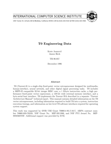
T0 Engineering Data. Version: 1.1.51 IntroductionT0 1 is a vector microprocessor, the rst implementation of the Torrent ISA. The Torrent Architecture Manual describes the Torrent ISA. This document is T0 speci c and provides the engineeringdata required to build a T0 chip into a system, timing information for T0 instruction execution,and information on low level T0 software interfaces required for operating system support.The overall structure of T0 is shown in Figure 1. The main components are a MIPS-II compatibleRISC CPU, an instruction fetch unit with an instruction cache, a system coprocessor (CP0), avector unit coprocessor (CP2), a 128-bit wide single cycle external memory interface, and a systeminterface port (SIP). In addition, T0 has two fast external interrupt pins, an internal counter/timer,and facilities for non-intrusive hardware performance monitoring.T0 is a single chip microprocessor implemented in a 1:0 m CMOS technology with a maximumclock frequency of 45 MHz. T0 can be run at lower clock rates to accomodate slower memorysubsystems. The CPU is a MIPS-II compatible 32-bit integer datapath. The CPU is used forgeneral scalar computation, and to support the vector unit by providing address generation andloop control. The instruction fetch unit manages a 1 KB instruction cache. The cache is directmapped with 64 lines each holding 4 instructions. The fast external memory interface together witha prefetching algorithm reduce instruction cache miss penalties. The maximum cache miss penaltyis 3 cycles, and the minimum is 0 cycles. The system coprocessor is implemented as coprocessor 0.CP0 provides exception handling, a 32-bit counter/timer, instruction cache management, and SIPI/O registers.The vector unit (VU) is added to the base MIPS-II architecture as coprocessor 2. The VU is avector register machine and contains 16 vector registers. Fifteen of these registers, vr1{ vr15, aregeneral purpose and hold 32 elements each 32 bits wide. There is also a zero register, vr0, that ishardwired to return the value 0. There are two vector xed point arithmetic functional units (VP0and VP1), each with 8 separate datapaths and capable of completing up to 8 32-bit arithmetic orlogical operations per cycle. The datapaths in VP0 can perform up to 8 16-bit 16-bit multipliesper cycle. VP1 does not include a multiplier, but otherwise the arithmetic units are identical.The arithmetic functional units can execute \arithmetic pipeline" instructions that chain up to6 arithmetic and logical operations within a single instruction. There is a single vector memoryfunctional unit (VMP), capable of sustaining up to 8 operand transfers per cycle. The externalmemory interface supports up to 4 GB of single cycle memory over a 128-bit data bus. AlthoughT0 issues only one instruction per cycle, it overlaps parallel and pipelined execution in multiplefunctional units to sustain a computational rate of 720 MOP/s 2 concurrently with a memorybandwidth of 360 M operands/s (720 MB/s).The system interface port (SIP) has a single control signal and an 8b data path in each direction.Functions accessed through SIP include chip testing, interrupt signalling, instruction cache invalidation, instruction single step, and DMA. Peak DMA rates over SIP to and from T0 memory are30 MB/s and 34 MB/s respectively at 45 MHz.12T0 is an abbreviation of Torrent-0.Up to 4.3 GOP/s using \arithmetic pipeline" instructions.
Figure 1: T0 Structure.
Figure 2: T0 CPU registers.T0 has a fully pipelined CPU that completes up to one instruction per cycle. T0 has the singleMIPS architected branch delay slot. There is a two cycle load-use delay, but both delay slots arefully interlocked.A hardware multiplier is provided that takes 18 cycles for a 32-bit 32-bit ! 64-bit integer multiply.There is a hardware integer divider that takes 33 cycles to perform a 32-bit 32-bit divide returningboth a 32-bit integer quotient and a 32-bit remainder. Integer multiplies and divides can proceedin parallel with other instructions provided the hi and lo registers are not read.All other CPU instructions apart from branches, loads, multiplies and divides, have single cyclelatencies and are fully bypassed so that their results may be used in the following cycle.In the Torrent architecture, vector memory accesses are unordered with respect to the CPU accesses,and with respect to each other. The MIPS-II SYNC instruction is used to guarantee the order ofmemory accesses. T0 processes all memory instructions in order, and the SYNC instruction has thee ect of waiting for the current memory instruction to complete. This can be used to synchronizeT0 memory accesses and host memory accesses over SIP, and also to wait for any pending vectormemory address errors.2.1 Operating ModesT0 has two operating modes: user mode and kernel mode. The current operating mode is storedin the KUC bit in the CP0 status register. The CPU normally operates in user mode until anexception forces a switch into kernel mode. The CPU will then normally execute an exception
8T0 Engineering Data. Version: 1.1.handler in kernel mode before executing a Restore From Exception (RFE) instruction to return touser mode.2.2 Emulated instructionsSeveral instructions in the MIPS-II instruction set are not implemented directly by T0. Theseinstructions are trapped and can be emulated in software by the trap handler.The misaligned load/store instructions, Load Word Left (LWL), Load Word Right (LWR), StoreWord Left (SWL), and Store Word Right (SWR), are not implemented. A trap handler canemulate the misaligned access. Compilers for T0 should avoid generating these instructions, andshould instead generate code to perform the misaligned access using multiple aligned accesses.T0 is not designed to operate as part of a shared memory multiprocessor and so the multiprocessorsynchronisation instructions, Load Linked (LL) and Store Conditional (SC), are not implemented.The MIPS-II trap instructions, TGE, TGEU, TLT, TLTU, TEQ, TNE, TGEI, TGEIU, TLTI,TLTIU, TEQI, TNEI, are not implemented. The trap handler can perform the comparison andif the condition is met jump to the appropriate exception routine, otherwise resuming user modeexecution after the trap instruction. Alternatively, these instructions may be synthesized by theassembler, or simply avoided by the compiler.The oating point coprocessor is not present on T0. All MIPS-II coprocessor 1 instructions aretrapped and can be emulated. For higher performance, compilers for T0 can directly generate callsto software oating point code libraries rather than emit coprocessor instructions. This will requirea modi ed MIPS calling convention.
9T0 Engineering Data. Version: 1.1.3 System Control Coprocessor (CP0)The system control coprocessor on T0 contains a number of registers used for host communication,the counter/timer, and exception handling. These registers are read and written using the MIPSstandard MFC0 and MTC0 instructions respectively. User mode can access the system controlcoprocessor only if the cu[0] bit is set in the status register. Kernel mode can always access CP0,regardless of the setting of the cu[0] bit. CP0 control registers are listed in Table 1.Number Register0 fromhost1 tohost2 vuepc3 vubadvaddr4{78 badvaddr9 count1011 compare12 status13 cause14 epc15 prid16{31DescriptionSIP input register.SIP output register.Vector unit exception program counter.Vector unit bad virtual address.unused.Bad virtual address.Counter/timer register.unused.Timer compare register.Status register.Cause of last exception.Exception program counter.Processor revision/implementation register.unused.Table 1: T0 CP0 control registers.3.1 Host Communication Registers31870fromhost870312402480tohost8Figure 3: Fromhost and Tohost Register Formats.There are two registers used for communicating and synchronizing with an external system overSIP. The fromhost register is an 8-bit read only register that contains a value written by the hostsystem over SIP. The tohost register is an 8-bit read/write register that contains a value that canbe read by the host system over SIP. The tohost register is cleared after reset to simplify host{T0synchronization. Their format is shown in Figure 3.
10T0 Engineering Data. Version: 1.1.3.2 Vector Unit Interrupt Registers310vuepc31320vubadvaddr32Figure 4: Vector Unit Exception PC and Bad Virtual Address Registers.The vector memory functional unit can generate an asynchronous interrupt when it encounters anaddress error on any element of a vector memory instruction. The ip5 bit of the cause register isa sticky bit that is set by any vector address error, and can only be cleared by explicitly writing tothe cause register. If both the im5 and iec bits of the status register are set, an interrupt will begenerated whenever ip5 is set. Refer to Section 7 for further details on interrupt handlng.The vupec register holds the program counter of the last vector memory instruction that had anaddress error and the vubadvaddr register holds the e ective virtual address that caused the fault.These registers are updated on any vector address error, even if vector address error interrupts arenot enabled. The vuepc register always points to the actual instruction that caused the fault, evenif the instruction was in a branch delay slot.Any vector address error stops execution of the current vector memory instruction, and leaves thestate of the vector registers and the vector ag registers unde ned. Execution cannot be restartedafter a vector address error, and so this interrupt is usually considered fatal to the running process.
11T0 Engineering Data. Version: 1.1.3.3 Counter/Timer Registers310count31320compare32Figure 5: Count and Compare Registers.T0 includes a counter/timer facility provided by the two coprocessor 0 registers count and compare.Both registers are 32 bits wide and are both readable and writeable. Their format is shown inFigure 5.The count register contains a value that increments once every clock cycle. The count register isnormally only written for initialization and test purposes. A timer interrupt is agged in ip7 inthe cause register when the count register reaches the same value as the compare register. Theinterrupt will only be taken if both im7 and iec in the status register are set. The timer interruptag in ip7 can only be cleared by writing the compare register. The compare register is usuallyonly read for test purposes.The count register is shadowed read-only in coprocessor 2 control register space as theregister.vcount
12T0 Engineering Data. Version: 1.1.3.4 Exception Processing RegistersA number of CP0 registers are used for exception processing.3.4.1 Status Register31 28CU4270121615IM887 602543210KUo IEo KUp IEp KUc IEc111111Figure 6: T0 Status Register FormatThe status register is a 32-bit read/write register formatted as shown in Figure 6. The statusregister keeps track of the processor's current operating state.The CU eld has a single bit for each coprocessor indicating if that coprocessor is usable. Bits 29and 31, corresponding to coprocessor's 1 and 3, are permanently wired to 0 as these coprocessorsare not available in T0. Coprocessor 0 is always accessible in kernel mode regardless of the settingof bit 28 of the status register. Both bit 28 and bit 30 may be on simultaneously.The IM eld contains interrupt mask bits. Timer interrupts are disabled by clearing im7 in bit 15.SIP interrupts are disabled by clearing im6 in bit 14. Vector address error interrupts are disabledby clearing im5 held in bit 13. External interrupt 0 is disabled by clearing im4 in bit 12. Externalinterrupt 1 is disabled by clearing im3 in bit 11. The other bits within the IM eld are not usedon T0 and should be written with zeros. Table 7 includes a listing of interrupt bit positions anddescriptions.The KUc/IEc/KUp/IEp/KUo/IEo bits form a three level stack holding the operating mode (kernel 0/user 1) and global interrupt enable (disabled 0/enabled 1) for the current state, and thetwo states before the two previous exceptions.When an exception is taken, the stack is shifted left 2 bits and zero is written into KUc and IEc.When a Restore From Exception (RFE) instruction is executed, the stack is shifted right 2 bits,and the values in KUo/IEo are unchanged.
13T0 Engineering Data. Version: 1.1.3.4.2 Cause Register31BD1300129 28CE227 1601215IP887620 ExcCode151002Figure 7: T0 Cause Register FormatThe cause register is a 32-bit register formatted as shown in Figure 7. The cause register containsinformation about the type of the last exception. Only the ip5 bit can be written, all other bitsare read only.The ExcCode eld contains an exception type code. The values for ExcCode are listed in Table 2.The ExcCode eld will typically be masked o and used to index into a table of software ost interrupt over SIP.Vector unit address error interrupt.Timer interrupt.Address or misalignment error on load.Address or misalignment error on store.Address or misalignment error on fetch.Syscall exception.Breakpoint exception.Reserved instruction exception.Coprocessor Unusable.Arithmetic Over ow.Vector Unit exception.Table 2: T0 Exception Types.If the Branch Delay bit (BD) is set, the instruction that caused the exception was executing in abranch delay slot and epc points to the immediately preceding branch instruction. Otherwise, epcpoints to the faulting instruction itself.If the exception was a coprocessor unusable exception, then the Coprocessor Error eld (CE)contains the coprocessor number. This eld is unde ned for any other exception.The IP eld indicates which interrupts are pending. Field ip7 in bit 15 ags a timer interrupt.Field ip6 in bit 14 ags an interrupt from the host over SIP. Flag ip5 in bit 13 ags a vector unitaddress error. Flag ip4 in bit 12 follows the external interrupt 0 pin, and ag ip3 in bit 11 followsthe external interrupt 1 pin. The other IP bits are unused in T0 and should be ignored when read.Table 7 includes a listing of interrupt bit positions and descriptions.
14T0 Engineering Data. Version: 1.1.3.4.3 Exception Program Counter310epc32Figure 8: EPC Register.is a 32-bit read only register formatted as shown in Figure 8. When an exception occurs, epc iswritten with the virtual address of the instruction that caused the exception, or if the instructionwas executing in a branch delay slot, the address of the branch instruction immediately precedingthe branch delay slot.Epc3.4.4 Bad Virtual Address310badvaddr32Figure 9: BadVAddr Register.is a 32-bit read only register formatted as shown in Figure 9. When a scalar memoryaddress error generates an AdEL or AdES exception, badvaddr is written with the faulting virtualaddress. The value in badvaddr is unde ned for other exceptions.Badvaddr
15T0 Engineering Data. Version: 1.1.3.5 Processor Revision Identi er310161615Imp887Rev80Figure 10: Processor Revision Identi er Register Format.The prid register is a 32-bit read only register that contains the implementation and revisionnumber of the CPU. These values can be used by con guration and diagnostic software.The prid register format is shown in Figure 10. Bits 15{8 de ne the implementation number, andbits 7{0 de ne the revision number. Bits 31{16 are reserved and return 0 on T0. The implementation number can be used by user software to detect changes in instruction set or performance. Therevision number identi es mask revisions of T0.Implementation eld values are given in Table 3.Imp. Number CPU0 T01-255 reservedTable 3: CPU Implementation types.
16T0 Engineering Data. Version: 1.1.4 Vector Unit Coprocessor 24.1 Vector registersT0 implements 16 vector registers, vr0{ vr15. Vector registers vr1{ vr15 are general purposeand each contain 32 32b elements. Vector register vr0 is hardwired to a vector containing 32elements with value 0. Reads of vr0 return 0, and writes to vr0 are ignored. Instructionsthat attempt to use the unimplemented vector registers, vr16{ vr31, cause a reserved instructionexception.T0 has two vector arithmetic functional units, VP0 and VP1, and a single vector memory functionalunit, VMP. Each functional unit can produce up to 8 results per clock cycle.4.2 Vector unit control registersThe vector unit control registers are listed in Table 4. Any CFC2/CTC2 instruction that attemptsto access an unimplemented vector control register will receive an illegal instruction exception.Number Register Descriptionvcr0 vrevImplementation/revisionvcr1 vcount Countervcr2 vlrVector lengthvcr4 vcond Vector condition agsvcr8 vovfVector over ow agsvcr12 vsatVector saturation agsTable 4: Vector unit control registers.
17T0 Engineering Data. Version: 1.1.4.2.1 VU Implementation and Revision Number (VCR0)310161615Imp887Rev80Figure 11: VU Implementation and Revision Register Format.The vrev register is a 32-bit read only register that contains the implementation and revisionnumber of the VU. These values can be used by con guration and diagnostic software.The vrev register format is shown in Figure 11. Bits 15{8 de ne the implementation number, andbits 7{0 de ne the revision number. The implementation number can be used by user software todetect changes in instruction set or performance. The revision number identi es mask revisions ofT0.Implementation eld values are given in Table 5.Imp. Number Vector Unit0 T01-255 reservedTable 5: VU Implementation types.
18T0 Engineering Data. Version: 1.1.4.2.2 Vector Length Register (VCR2)3180247 0vlr8Figure 12: Vector Length Register Format.The length of a vector operation is speci ed in an 8-bit vector length register, vlr. If a vectorinstruction is issued when the value in vlr is 0, no operations are performed. If a vector instructionis issued when the value in vlr is greater than 32, a vector length error exception is raised.Reads or writes of the vector length register do not a ect vector instructions in progress.4.2.3 VU Counter (VCR1)31vcount320Figure 13: Vector Count Register Format.The VU count register, vcount, is a 32-bit read-only register that holds a cycle counter. It shadowsthe count register in coprocessor 0. The count value is incremented once per clock cycle regardlessof host SIP activity, instruction cache misses, or interlocks.4.2.4 VU Condition Register (VCR4)31vcond320Figure 14: Vector Condition Register Format.The VU condition register, vcond, is a 32-bit read/write register as shown in Figure 14.The vcond register is only altered by vector set less than instructions, vector set equal instructions,and CTC2 writes of vcond. After execution of a vector comparison instruction, each bit of vcondholds the result of the comparison for each element of the destination vector register. Bit x holdsthe result of the comparison for element x.
19T0 Engineering Data. Version: 1.1.4.2.5 VU Over ow Register (VCR8)31vovf320Figure 15: Vector Over ow Register Format.The VU over ow register, vovf, is a 32-bit read/write register as shown in Figure 15. The vovfregister contains 32 sticky bits holding the over ow status for signed integer adds and subtracts.The vovf register is only altered by vector signed add (ADD.yy) and vector signed subtract(SUB.yy) instructions, and control to coprocessor writes of vovf. If any result of a ADD.yy orSUB.yy instruction over ows, the corresponding bit of vovf is set. Bit x holds the over ow statusof element x. The over ow bits can only be reset by a CTC2 write of vovf.4.2.6 VU Saturation Register (VCR12)31vsat320Figure 16: Vector Saturation Register Format.The VU saturation register, vsat, is a 32-bit read/write register as shown in Figure 16. The vsatregister contains 32 sticky bits holding the saturation status for xed point adds (FXADD.yy),subtracts (FXSUB.yy), and multiplies (FXMUL.yy).The vsat register is only altered by FXADD.yy, FXSUB.yy, and FXMUL.yy instructions, andCTC2 writes of vsat. If any result of a FXADD.yy, FXSUB.yy, or FXMUL.yy instruction saturates,the corresponding bit of vsat is set. Bit x holds the saturation status of element x. The saturationbits can only be reset by a CTC2 write of vsat.
20T0 Engineering Data. Version: 1.1.5 Instruction EncodingsFigures 17, 18, and 19 detail the opcode decoding for T0. A key to the symbols appears below.* Opcodes marked with an asterisk cause a reserved instruction exception. Opcodes marked with a xi are illegal but do not cause a reserved instruction exception. Opcodes marked with a phi cause a coprocessor 1 unusable exception. Opcodes marked with a delta cause a coprocessor 2 unusable exception if the CpU2 bit in thestatus register is clear, otherwise they cause a reserved instruction exception. Opcodes marked with a sigma cause a reserved instruction exception if opers (bit 10) is set. Opcodes marked with a rho cause a reserved instruction exception if the register number in rddoesn't match a coprocessor 2 control register as listed in Table 4. Opcodes marked with a theta cause a coprocessor 3 unusable exception.
Figure 17: T0 CPU Instruction Encodings.
Figure 18: T0 Coprocessor 0 Instruction Encodings.
Figure 19: T0 Vector Instruction Encodings.
Figure 20: T0 virtual address space.In kernel mode, the processor can access any address in the entire 4 GB virtual address space.In user mode, instruction fetches or scalar data accesses to the kseg segment are illegal and causea synchronous exception. The AdEF exception is generated for an illegal instruction fetch, andAdEL and AdES exceptions are generated for illegal scalar loads and stores respectively. In usermode, vector data memory accesses to the kseg segment cause an asynchronous vector unit addressinterrupt to be agged in ip5 in the cause register. For both scalar and vector stores, no datamemory will be written at the faulting address. A faulting vector memory operation will cause thestate of the vector unit to become unde ned.There is no memory translation hardware on T0. Virtual addresses are directly passed as physicaladdresses to the external memory system. The external memory system may simply ignore unusedhigh order address bits, in which case each physical memory address will be shadowed multipletimes in the virtual address space.On each memory cycle, T0 outputs information regarding the type (instruction/data, kernel/user,read/write) of each memory access as well as the physical memory address. This information canbe used by an external memory protection system to provide ner grain memory protection. Forexample, user memory access may be restricted to a single shadow of the real physical memory.The external memory protection system can signal faults by interrupting T0.
T0 Engineering Data. Version: 1.1.257 Reset, Interrupt, and Exception ProcessingThere are three possible sources of disruption to normal program ow: reset, interrupts (asynchronous
terface p ort (SIP). In addition, T0 has t w o fast external in terrupt pins, an in ternal coun ter/timer, and facilities for non-in trusiv e hardw are p erformance monitoring. T0 is a single c hip micropro cessor implemen ted in a 1: 0 m CMOS tec hnology with a maxim um clo c k frequency of 45 MHz. T0 can b e run at lo w er clo c k rates to .