Transcription
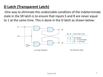
D Latch (Transparent Latch)-One way to eliminate the undesirable condition of the indeterminatestate in the SR latch is to ensure that inputs S and R are never equalto 1 at the same time. This is done in the D latch as shown below:Lecture 261
-This latch has only two inputs: D (data) and En (enable). The D inputgoes directly to the S input, and its complement is applied to the Rinput. As long as the enable input is at 0, the cross-coupled SR latchhas both inputs at the 1 level and the circuit cannot change stateregardless of the value of D .-The D input is sampled (tested) when En 1. If D 1, the Q outputgoes to 1, placing the circuit in the set state. If D 0, output Q goes to0, placing the circuit in the reset state.Lecture 262
-The D latch receives that designation (title) from its ability to holddata in its internal storage. It is suited for use as a temporary storagefor binary information between a unit and its environment.-The binary information present at the data input of the D latch istransferred to the Q output when the enable input is asserted(confirmed). The output follows changes in the data input as long asthe enable input is asserted.Lecture 263
-This situation provides a path from input D to the output, and forthis reason, the circuit is often called a transparent (clear) latch.When the enable input signal is de-asserted, the binary informationthat was present at the data input at the time the transition occurredis retained (i.e., stored) at the Q output until the enable input isasserted again.Lecture 264
-Note that an inverter could be placed at the enable input. Then,depending on the physical circuit, the external enabling signal will bea value of 0 (active low) or 1 (active high).-The graphic symbols for the various latches are shown below. A latchis designated by a rectangular block with inputs on the left andoutputs on the right. One output designates the normal output, andthe other (with the bubble designation) designates the complementoutput.Lecture 265
-The graphic symbol for the SR latch has inputs S and R indicatedinside the block. In the case of a NAND gate latch, bubbles are addedto the inputs to indicate that setting and resetting occur with a logic0 signal. The graphic symbol for the D latch has inputs D and Enindicated inside the block.Lecture 266
Storage Elements: Flip-flops-The state of a latch or flip-flop is switched by a change in the controlinput. This momentary change is called a trigger, and the transition itcauses is said to trigger the flip-flop.-The D latch with pulses in its control input is essentially a flip-flopthat is triggered every time the pulse goes to the logic-1 level.-As long as the pulse input remains at this level, any changes in thedata input will change the output and the state of the latch.Lecture 267
As seen from the block diagram above, a sequential circuit has afeedback path from the outputs of the flip-flops to the input ofthe combinational circuit. Consequently, the inputs of the flipflops are derived in part from the outputs of the same and otherflip-flops.Lecture 268
Edge-Triggered D Flip-FlopThe construction of a D flip-flop with two D latches and an inverter isshown below:The first latch is called the master and the second the slave. Thecircuit samples the D input and changes its output Q only at thenegative edge of the synchronizing or controlling clock(designated as Clk ).Lecture 269
-When the clock is 0, the output of the inverter is 1. The slave latchis enabled, and its output Q is equal to the master output Y . Themaster latch is disabled because Clk 0. When the input pulsechanges to the logic-1 level, the data from the external D input aretransferred to the master. The slave, however, is disabled as long asthe clock remains at the 1 level, because its enable input is equalto 0. Any change in the input changes the master output at Y, butcannot affect the slave output.Lecture 2610
-When the clock pulse returns to 0, the master is disabled and isisolated from the D input. At the same time, the slave is enabledand the value of Y is transferred to the output of the flip-flop at Q .Thus, a change in the output of the flip-flop can be triggeredonly by and during the transition of the clock from 1 to 0.Lecture 2611
The behavior of the master–slave flip-flop just described dictatesthat:(1) the output may change only once,(2) a change in the output is triggered by the negative edge ofthe clock, and(3) the change may occur only during the clock’s negative level.The value that is produced at the output of the flip-flop is thevalue that was stored in the master stage immediately before thenegative edge occurred .Lecture 2612
-It is also possible to design the circuit so that the flip-flop outputchanges on the positive edge of the clock. This happens in a flip-flopthat has an additional inverter between the Clk terminal and thejunction between the other inverter and input En of the master latch.Such a flip-flop is triggered with a negative pulse, so that the negativeedge of the clock affects the master and the positive edge affects theslave and the output terminal.Lecture 2613
-Another construction of an edge-triggered D flip-flop uses three SRlatches as shown below. Two latches respond to the external D (data)and Clk (clock) inputs. The third latch provides the outputs for theflip-flop. The S and R inputs of the output latch are maintained at thelogic-1 level when Clk 0.Lecture 2614
This causes the output to remain in its present state. Input D maybe equal to 0 or 1. If D 0 when Clk becomes 1, R changes to 0.This causes the flip-flop to go to the reset state, making Q 0. Ifthere is a change in the D input while Clk 1, terminal R remainsat 0 because Q is 0.Lecture 2615
Thus, the flip-flop is locked out and is unresponsive to furtherchanges in the input. When the clock returns to 0, R goes to 1,placing the output latch in the quiescent condition withoutchanging the output. Similarly, if D 1 when Clk goes from 0 to1, S changes to 0. This causes the circuit to go to the set state,making Q 1. Any change in D while Clk 1 does not affect theoutput.Lecture 2616
In sum, when the input clock in the positive-edge-triggered flip-flopmakes a positive transition, the value of D is transferred to Q . Anegative transition of the clock (i.e., from 1 to 0) does not affect theoutput, nor is the output affected by changes in D when Clk is in thesteady logic-1 level or the logic-0 level. Hence, this type of flip-flopresponds to the transition from 0 to 1 and nothing else.Lecture 2617
-The timing of the response of a flip-flop to input data and to theclock must be taken into consideration when one is using edgetriggered flip-flops. There is a minimum time called the setup timeduring which the D input must be maintained at a constant valueprior to the occurrence of the clock transition.-Similarly, there is a minimum time called the hold time during whichthe D input must not change after the application of the positivetransition of the clock. The propagation delay time of the flip-flop isdefined as the interval between the trigger edge and the stabilizationof the output to a new state. These and other parameters arespecified in manufacturers’ data books for specific logic families.Lecture 2618
-The graphic symbol for the edge-triggered D flip-flop is shown inthe figure above. It is similar to the symbol used for the D latch,except for the arrowhead-like symbol in front of the letter Clk,designating a dynamic input. The dynamic indicator ( ) denotesthe fact that the flip-flop responds to the edge transition of theclock. A bubble outside the block adjacent to the dynamicindicator designates a negative edge for triggering the circuit.The absence of a bubble designates a positive-edge response.Lecture 2619
specified in manufacturers' data books for specific logic families. Lecture 26 18. Lecture 26 19-The graphic symbol for the edge-triggered D flip-flop is shown in the figure above. It is similar to the symbol used for the D latch, except for the arrowhead-like symbol in front of the letter Clk,