Transcription
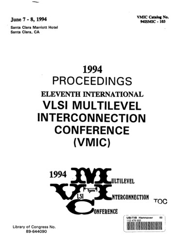
T n n e 7 - R 1994june / - », iyy*VMIC Catalog No.MEMIC -103Santa Clara Marriott HotelSanta Clara, CA1994PROCEEDINGSELEVENTH INTERNATIONALVLSI CONNECTION(INFERENCEUB/TIB Hannover112 479 502Library of Congress No.89-64409089
C. "Fluorine-Implanted Treatment (FIT) SOO for the Non-EtchbackIntermetal Dielectric" by L.-J. Chen, S.-T. Hsia, and J.-L. Leu; ERSO/ITRI; Taiwan. R.O.C.D. "A Sub-micron Paiylene Etch Process for Multilevel Interconnections"by X. Zhang, R. Tacito, C. Steinbruchel, and JJ . McDonald; RPI; Troy, NY;VJS. Yaney, AT&T BELL LABS; AUentown. PA; and C Chiang; INTELCORP; Santa Clara, CA. . ' . .E. "An Interlayer Dielectric Films Formation Technology Using TEOS/O, APCVD SiO, FUms on Dual Frequency TEOS/O- PECVD SiO.Films" by A, Knbo, K. Hirose, T. Honuna and Y. Murao; NEC CORP;Kanagawa, JAPAN.F. "A Study or Plasma Treatments on SHozane SOG" by C.K.Wang, H. C. Huang. LM. Uu, and M. S. Lin; TSMC; Taiwan. R.O.C.; andH.C. Cheng, CHIAO-TUNG UNTV; Taiwan, R.O.CELEVENTH INTERNATIONALVLSI MULTILEVEL INTERCONNECTIONCONFERENCEJune 7-8,1994ADVANCE PROGRAMTuesday, June 7,1994OPENING SESSION—9 A.M.Welcoming Remarks and General CommentsDr. Thomas E. WadeG.University of South FloridaH.SESSION I — 9 : 1 5 A.MKEYNOTE ADDRESS"THE CHALLENGES OF THE MULTILEVELINTERCONNECT TO THE EQUIPMENT INDUSTRY"Dr. Dan MaydanPresidentAPPLIED MATERIALS CORP.Santa Clara, CACoffee Break 9:45-10 AM.SESSION n - 1 0 A.M.-12 NoonVLSI MULTILEVEL INTERCONNECTIONCOMPLETE PROCESS REALIZATIONDr. David B. FraserINTEL CORP.Santa Clara, CAA. a,H,Shibata,M. Kakumu. K. Mori, K. Otsuka, M. Takahashi, N. Kaji, M. Kodera, K.BchJlNagata, and R-Aoid; TOSHIBA; Kawasaki. JAPAN. . . .B. "A High Performance 0.5-micron Five-Level Metal Process withExtendability to Sub-Half Micron Devices" by M E Chisholm, GA .DixiUMX Jain and R.H. Havemann; TEXAS INSTRUMENTS:DaUas,TX.C A Low Cost 0.7 Micron Triple Level Metal Interconnect Process forAdvanced BiCMOS Technology" by R.WaU,B.Lowe and M. Phillips;PHILIPS SEMICONDUCTORS; Albuquerque, NM.D. "An Advanced Multilevel Interconnection Technology for 035 Micron High Performance Devices" by CS. Pal, CT. Uu, CB. Case, W.YC Lai, CJ. Case, J. M. Miner, S.C. McNevin, N A CSampa, and R. Liu;AT&T BELLLABS; Murray Hill, NJ.E. "A Low-Temperature Local Interconnect Process In a 0.25-micronChannel CMOS Logic Technology with Shallow Trench Isolation" byJ. Oivens, S. Oeissler, O. Cain. W. dark, C Koburger, and J. Lee; IBM;EssexJcUVT.F. Dual Damascene Copper Metallization Process Using Chemical Mechanical Polishing" by S. Lakshminarayanan, J. Steigerwald, D. Price,M. Bourgeois, T.P. Chow, R.J. Gutmann, and S.P. Murarka;RENSSELAER POLYTECHNIC INST.; Troy, NY.*— POSTER PAPERS —G. "Multilevel Metallization for ASIC Technology" by S. Lee, K. Lee,H.Oh,and D.Kim;SAMSUNG;Suwon,KOREA. . . .H. 'The Rear End Process for OS micron 16M DRAM/4M SRAM" byS-T. Hsia, K-C Chen. L-J. Chen. J-N. Kuo, C-Y. Lee and C-J. Kuo;ERSQ/rrRI; Taiwan, R.O.CLJ.K.13L.Chairman;SESSION H I . 1:30 - 3 3 0 RM.VLSI MULTILEVEL INTERCONNECTIONDIELECTRIC PROCESSESChairman;M.152229O.P.—SPECIAL NOTES —"Investigations on Instability of TEOS-O, BPSG FUms by the Photoresist Stripping Treatment" by N J i Park, S.R. Song. SJ. Choi, J.S. Bvun,K.G. Rha, JjTKim and W.S. Kim; GOLDSTAR; Cheongju-Si, KOREA."Crystal-Free and Low Flow Angle ILD by Using In-Sltu SACVD/PEBPSG for OS micron Applications" by H.-C. Yen. B.-Y. Jin, C. Wong, P.Chow, D. Yen; MACROMX; Taiwan, R.O.C.; J. Hu, J. Su. K.-Y. Uao, S.Chen, andJ. Wang; APPLIED MATERIALS; Taiwan; R.OXJ. . . ."The Deposition of Low Dielectric Constant FUms UslngTEOS/Ozonebased,Chemistry" by Y. Yuyama, N. Tokumasu, and IC Maeda, SEMICONDUCTOR PROC. LAB; Tokyo, JAPAN; J. Foggiato, J. Park, S. Fisher.QUESTER TECH; Fremont, CA. . . . . T"Reflow Characteristics of High Deposition Rate CVD O.TEOS BPSGFilms" by V. Siva, M. Galiano, S. Robles, V. Kithcart, B. C. Nguyen;APPLIED MATERIALS; Santa Clara, CA; and Y.H. Kim. APPLIEDMATERIALS; JAPAN.87.94101Ill1 14117, „12012121 31132133134364349596265Dr. Loren W. T.inholmNATLINST. OF STD. & TECS.Gaithersburg, MDA. "Highly Reliable Silicon Oxynltride Film Formed by Biased ECR CVDfor Interlayer Dielectric of Multilevel Interconnections" by H. Ishlkawaand Y.Murao; NEC CORP. Kanagawa, JAPAN.B. "Comprehensive Investigation of the Impact Dopant Concentration onthe Chemical, Mechanical, and Electrical Properties on Doped GlassFilms" by Y. S. Obeng, T. J. Smith. D. C Brady. KJ3. Steiner. R Chew, andJA. Simmons; AT&T BELL LABS; Auentown. PA.N.—POSTER PAPERS —"Interlevel Dielectric Engineering for Improved Device Performancein Hair-Micron CMOS" by L. Forester, G. Van den bosch, R Meynen, B.Coenegrachts, L. Van den hove; IMEC; Leuven, BELGIUM; andT. Collins;ALCATEL MlETEC;Oudenaarde.BELaiUM."Gap-Fill for Sub-0.5 micron Technologies: Process and Cost Considerations for Spin-On Glass" by CB. Case. C. J. Case, GJ. Schwartz; AT&TBELL LABS, Murray Hill. NJ; and KM. Rutherford; ALLIED SIGNAL;SantaClara,CA"Evaluation of Germanium-Doped Silicon Dioxide FUms Used for Advanced ULSI Applications" by R. Thakur, R. Iyer, MICRONTECR; Boise,ID; S. Fisher, QUESTER TECH.; Fremont, CA; N. Tbkumasu. K. Maeda,Y. Nishimoto; SEMICONDUCTOR PROC. LAB; Tbkyo, JAPAN. . ."A Non-Etch Back Spin-On Glass for 0.5 micron Devices Using Hydrogen Sllsesquloxane as a Replacement for Methylslloxane" by B. T.Ahlbum;TEXAS INST.; Dallas, TX; and KA. Scheibert; DOW CORNING; Midland, ML"Characterization or Boron and Phosphorus Doped Germanium Sillcon Oxide FUmsforInterlevel Dielectric Applications" by N. Tokumasu,K. Maeda, Y.Nishimoto;SEML PROCESS LAB;Tbkyo. JAPAN; K.Tanaka;CANON; Tokyo, JAPAN; and S. Fisher; QUESTER TECH.; Fremont,CA,"Thermal Conductivity of Thermally Grown and TEOS-CVD FUms inVLSI/ULSITechnologles"byA l. SaxenalNST.MIKROELEKTRONIK;Stuttgart, GERMANY; M Bourgeois;R.PJ.; Trcpy, NY; and HA. Schaffl,J.S. Seuhle and J. Albert; NATL&JST. STD. & TECH.; Gaithersburg, MD.816774SESSION IV-3:45-6:25 P.M.VLSI MULTILEVEL INTERCONNECTIONPLANARIZATION PROCESSES135Chairman: Dr. Michael E. ThomasNATIONAL SEMI/FA1RCHILD RES. CTR.Santa Clara, CAA. "Improved SOG Process Compatible with 6-level Metallization" byN.Ohashi, H, Nezu,T.Fujiwara and N.Owada; HITACHI; Tokyo, Japan.B. "Improved Multilevel Metallization Technology Using ChemicalMechanical Polishing of W Plugs and Interconnects" by C.C. Yu. JKlein and Y. Limb; MOTOROLA; Austin.TX. . . . . . . .C "Resist Etch Back as a Manufacturable Low Cost Alternative toCMP" by B. Neureuher, F. Binder, B. Fischer, Z. Gabric, K. KoUer and SRohl; SIEMENS AG; Munich, GERMANY.D. ntaCUra.CA.E. "Single Step Global Planarlzatlon Using a Super Self-Flow O HMCTSZ PECVD Dielectric" by R Nishio, A. Shimlzu. K. Watanaoeand ICKobayashl; FUJITSU LTD; Kawasaki, JAPAN.F. "Development of a Global Planarlzatlon Process without CMP" by L.Forester. B. Coenegrachts, M. Stone, H. Meynen. and L. Van den Hove;IMEC; Leuven, BELGIUM.G "CMP Planarlzatlon of Poly-Metal and Inter-Metal Dielectrics for 0.35micron CMOS Multilevel Interconnection Technology" by W.Y-C. Lai,J. F. Miner, C S. Pal, C. T. Iiu, C B. Case and R. Liu; AT&TBELLLABSMurray HULNJ.H. "New Reflowable Organic Spin-On GlassforAdvanced Gap-Filling andPlanarlzation" byT.FuTdsawaandY. Homma; HITACHI; Tokyo, JAPANand Y. Shimamura, R Morishlma, Y. Yamamoto and R Satoh; HITACHICHEMICAL CO.; Ibaraki. JAPAN. . .137144151158165172179186
—POSTER PAPERS —L "Effect of Underlayers on High Temperature Aluminum PlanarizatlonProcess" by K-C. Chen, S-T. Hsia, J-N. Kuo, R Yen and CrY. Lee; ERSO/ITRI; Taiwan, R.O.C195J. "Applications of Atomic Force Microscopy to Quantifying dS.Bothra;VLSITBCHlyaNOLOGY; San Jose, CA.K. "Aluminum PlanarlzatlonforSub-micron Devices Using a High Ternperature Two Step Aluminum Process" by EJJL Chiang, K.C. Wang;WINBOND ELECTRONICS; Taiwan, ROC and D. Lee, J. Carmody andA. Helms Jr.; VARIAN, Palo Alto, CA.201L. "Silicon Contact Formation and Photoresist Planarlzatlon Using Chemical Mechanical Polishing" by C. L. Keast, R. B. Goodman, M.W. Hornand R.R.Kunz; MASS. INST. OF TECH.; Lexington, MA. . . .204M. nULSIProccssbisrbyM.aien.S-T.HsUandK XCbBn;ERSCVina;Taiwan,R.O .206N. "Study of Multilayer Thick P-SOG Interpoly Planarlzatlon In Submlcron Technology" by LXLu, L. Nguyen. Y.S. Lin, G. Smith and F.T. Iiou;SGS-THOMSON;CarroUton,TX209— SPECIAL NOTES —O. "Selective 0,-TEOS LPCVD Process for In-Sltu Planarlzatlon in Multilevel MetaUizaUons" by A.N. Saxena; LS.C. and RJPX; M. Bourgeoisand G. Martin; R J i ; Troy, NY.215P. "Characterization of Chemical Mechanical PolishingforPlanarlzatlonof Interlevel Dielectric In Superconducting Circuits" by M. Bhushan, R.Rouse and JJ2. Lukens; SUNY; Stony Brook, NY.216Q. "APCVD TEOS/O. Thin Film Integration into Multilevel InterconnectProcess Modules" by J. P. West; MOTOROLA; Austin, TX; T. O. KINS-JOHNSON;Scotts Valley, CA.217R. "Wear Mechanism In Inter Level Dielectric PlanarlzaOon by ChemicalMediank Polishing" by CFiuitman;SPEEDFAM CORP; Chandler, AZ;andS.Davis,M.DesaLandR. Jalrath; SEMATECH;Austin,TX. - 1 Wednesday, June 8,1994SESSION V - 8 : 0 0 - 1 0 : 4 0 A.MVLSI MULTILEVEL INTERCONNECTIONRELIABILITY ISSUESChairman-219Dr. Philip J. FlemingAPPL. UNLIMITEDColorado Springs, COA. "A Novel Stress Measurer In Real-Time on Entire-Wafer and Its AppUcations in Multilevel Interconnections" by G. Wu, L. Xu, W. Chen, g.CHINA.B. "Plasma Induced Damage During Contact Etch Process Using Mechanical and Electrostatic Chucks" by T.T. Nguyen and V. Bissessur,SEMATECH; Austin. TX.C. "Moisture-Blocking Mechanism or ECR-Plasma SIO, and High Reliability Performance of Multilevel AL Metallization''by M. Dokl, RWattlani, and Y. Furumura; FUJITSU LTD; Kawasaki. JAPAN; and S.Okuda; FUJITSU LTD; Mie, JAPAN.D. "Extrusion Related Short Circuit Failure hi Submlcron Interconnects"by V.ChowdhuryandD.Pramanik; VLSI TECHNOLOGY; San Jose, CA.E. "High-Frequency Electromlgratlon Test Using T.HoriuchiandK.Okumura;NECCORP; Kanagawa; JAPAN.F. "Effect of ILD's on the Residual Resistivity and the Reliability of AlBased Interconnects" by A. N. Saxena; ISC and RJX: Ballston Lake, NY;andK.Ramkumar and S.K. Ghosh; RENSSELAER POLYTECHNIC JNST,Troy.NY.G. "Inter-Metal Dielectric Adhesion Improvement After SOG Etch Backfor Multilevel Interconnection Devices Using Blanket Tungsten for andLZanotn;SGS-THOMSON;Milano, ITALY.H. "Permitted Electromlgratlon of Tungsten-Plug Vlas in ChainforTestStructure with Short Inter-plug Distance" by T. Aoki and T. Nogami;KAWASAKI STEEL; Chiba-city, JAPAN.—POSTER PAPERS —L "Effects of TOWl Cap Layers on Improving Electromlgratlon In AlBased Multi-layered Interconnects" by Y. Inoue, S-I. Tanimoto, K.Tsujimura, T. Yamashlta, Y. Ibara, Y. Yamashita, and K. Yoneda; SANYO;GuXJAPAN.J. "Interaction of Titanium Cap and Aluminum Alloys with TIN BarrierLayer on Annealed Metal Sheet Resistance and on ElectromlgratlonPerformance" by K. Hewes, D. Yost, HA. Le, J.W. McPhenon; TEXASINSTRUMENTS; Dallas. TXK. "Mechanism Approached the SOG Degassing TechniqueforULSI Production by Using RGA Method" by L-J. Chen. K-C. Chen and S-T. Hsia;ERSO/ITRI; Taiwan, R.O.C. L. "Formation Mechanism of Ring Defects During Metal RUE" by E.O. Colgan, S. Greco, N. Greco and JJ. White; IBM; EastFishkilL NY. . .M. a;SHARPCORP.;NsrUAPAN.622 1o 2o 2o „ c235N. "Damage to Gate Oxide from Interconnect Processing" by C Gabriel,M. Weling, and S. Davis, M. Desai, and R. Jairath; SEMATECH; Austin,TX. and S.Bothra; VLSI TECHNOLOGY; San Jose, CA.O. "The Improvement of SM and EM Resistances in Double Metal Process" by S.C. Shim. E. Kim, K.W. Jo, OB. Jeong, C.S. Song. SJC. Lira andK.R Choi; SAMSUNG; Kyunggi-Do, KOREA.P. "Process-Induced Contamination of Spln-on-Glass Planarizatlon Layers after Etchback Processing" by P.F. Skowronski, A. Shepela, W.CHarris. L. LeTarte and D. O'Connor. DIGITAL EQUIPMENT CORP.;Hudson,MA.Q. "Moisture Trapping and Plnhole Suppression by the Use of High Refractive Index PECVD SiO,Thin Film" by P. Lee, B. Pang, J. Huang, CNgai and D.Cheung; APPLIED MATERIALS; Santa Clara, CA. . . .R. "AC Electromigratlon on Via Structures" by L M. Ting; TEXAS INSTRUMENTS; Dallas, TX.S. "The Formation Mechanism or Metal Pillar by Plasma Etch and ItsRemoval Methods" by D-W. Yun. & Kim. C-B. Jeong. S-K. Han, S-K.Lira and K-RChoU SAMSUNG ELECTRONICS; Kyunggi-Do,KOREA.—SPECIAL NOTES—T. "A Via Corrosion in THB Stress Test" by C. Chou; WINBONDELECTRONICS; Taiwan, R.O.C.U. "Reduction of Electrical Damage and Particle Contamination UsingICP Soft Etch for Pre-MetaUization Cleaning of Advanced MOS Devices" by J. Sasserath and M Namaroff; MATERIALS RESEARCH;Congers, NY; and T. Yanagida, H. Sumi, and Y. Sugano; SONY;Kanagawa-ken, JAPANV. "The Effect of Deposition and Annealing Conditions on the Stressin Metallization Materials for VLSI Interconnects" by A. Witvrouwand K.Maex; IMEC; Leuven. BELGIUM.W. "Electromigratlon Performance of TIN/Ti/Al/TiN MetallizationSystems" by T. Yamaha, M. Naito and T. Hotta; YAMAHA CORP.;Shizuoka, JAPAN.X. "Elimination of Solvent-Induced Corrosion on Fluorine Contaminated Bonding Pad Surfaces" by K. Mautz, M. Hall and J.Cadenhead IOTOROLA; Austin. TX.Y. "The Elimination of Moisture in TEOS/Ozone Dielectrics for 0.35micron Applications" by S. Fisher, J. Park, and J. Foggiato; QUESTERTECH.; Y. Nishimoto, N. Tokumasu, K. Jujino and K. Maeda;SEMICON-DUCTOR PROCESS LAB; Tokyo, JAPAN. . . . .Z. "PartideEmission from TargetsDurhig Sputter Deposition of Aluminum Alloy Thin Films" R.S. Bailey, A. Leybovich, J. E. Poole, T.Kuniya, N.C. Hill, and CJE. Wiekersham, Jr.; TOSOH SMD; GroveCity, ORAA. "Improving Passivation Integrity or Reducing Plnhole Counts" byE.Sabin; SILICON SYSTEMS; Santa Cruz, CA.BB. "Edge Cracking Induced Particles for SOG EBR Processing" byL-J. Chen, K-C. Chen, S-T. Hsia and C-Y. Lee; ERSO/rrRI; Taiwan,R.O.C.CC. "Control of Field Threshold Voltage Through Optimization ofPECVD Oxide Process Conditions" byJ.Dun,S.Tai,D.Wbiteside.D. Dang and R. Chuang; SEJCONK; Santa Clara. CA. . . . .SESSION VI-10:55 A.M.-12 NoonVLSI MULTILEVEL INTERCONNECTIONPOSTER PAPER, SPECIAL NOTE ANDEXHIBITION VIEWING240„2.4 e , 252.259266AWARDS LUNCHEON-12-2:00 RM. ."National Technology Roadmap for Semiconductors"Dr. Robert M. BurgerVice President & Chief ScientistSEMICONDUCTOR RESEARCH CORPORATIONResearch Triangle Park, NCSESSION V H - 2 : 0 0 - 5 : 0 0 P.M.VLSI MULTILEVEL INTERCONNECTIONCONDUCTOR SYSTEMSChairman:„n o278.o 17318319320321. 323327Dr. Terry O. HemdonMIT LINCOLN LABSLexington, MA1. CONTACT AND VIA FILLING SYSTEMSA. Deep-Submlcron Plug AppUcatlons and Process Using UHV Cluster Tool" by T.Ohta, N. Takeyasu, E. Kondoh, Y. Kawano and R Yamaoto; KAWASAKI329STEEL CORP.; Chiba, JAPAN.
SESSION VJJ ContinuedB. "Influence ofTI, TIN and TlSL.Underlayers on Al-Sl-CuReflowSput- .terlng" by N. Ito, Y. Yamada, and Y. Murao; NEC CORP.; SagamiharaCity, JAPAN; and D.T.C. Huo; AT&T BELL LABS; Murray Hill, NJ. .336C "Use of NISItothe Self-Allgned-SUlclde (SALJODE) Process for DeepSubmlcrometer Devices" by R. Mukai, S. Ozawa, H. Yagl and H.Tsuchikawa; FUJITSU LTD.; Kawasaki, JAPAN.343—POSTER PAPERS—D. "Multilevel Interconnect for ASIC: Impact of Post Etch Treatment toAchieve Low Via Resistance" by T. T. Nguyen and C.F. Hoener,SEMATECH; Austin, TX; and SJ. Kirk and C.Y. Tie; EKCTECHNOLOGY;Hayward,CA353E. "Advanced Etching Process for Sub-micron Contact Using High Energy Ion Implantation" by WJ. Lee, K.R Lee, S.R Yu, J.S. Baik, CO.Ko,C.R Lee and SJL Choi; HYUNDAI; Kyungki-do. KOREA. . . 3 5 6F. "Borderless Contacts for 64M DRAM Using a Sacrificial Mandrel" byE Kiewra, W. Cote, D. Hunt, W. Kocon, D. Restaino, N. Giammarco, andC Radens; IBM; HopeweU Jet, NY; E. Eckstein; SIEMENS; Cedex,FRANCE; K. Wangemann. K. Feldner, and W. Henkel; SIEMENS AG;HopeweU Jet, NY; andS.Roeht SIEMENS AG; Munich, GERMANY. . 3 5 9G. "Selective Chemical Vapor Deposition of Aluminum at Low TemperatureforSubmlcron Contact and Via Hole Filling" by M.R Tsai and S.CSun;CHIAOTUNG UNIV.;Taiwan,R.O.C362H. "Chemical Vapor Deposition of a Contact Resistance Enhancing Layer"by J.T. HUbnan, R.F. Foster, J. Faguet and R. Arora; MRC, Phoenix, AZ.;and C Arena, D'BTUDES NUCLEATES; Grenoble, FRANCE . .365L "Characterization or DCS Reduced W Siliclde Formed at Mid-TemperatureforULSI Device" by CJL Woo, VS. Kang, J.W. Lee, K-H.Suh, S.Y. Ko, Y. Lira, and B.W. Yoon; GOLDSTAR ELECTRON;Cheongju-Si, KOREA.368J. "Submlcron Contact Hole Filling Using Hot Aluminum: Profile Evolution and Physical Modeling" by T. Smy; CARLETON UNTV; Ottawa,CANADA; S.K. Deew and M J. Brett; UNIV. OF ALBERTA; Edmonton.CANADA; W. Tsai and M. Biberger, VARIAN; Palo Alto, CA; and K.C.Chen and S.T. Hila; ERSO/ITRI; Taiwan, R.O.C371K. IDevIces"by K-C. Chen, S-T. Hsia. J-N. Kuo, R Yen. C-Y. Lee and C-J. Kuo; ERSO/mU; Taiwan, R.O.C.374L. "Electrical and Physical Characteristics or a Multi-Level Via StructureConsisting or Deep and Shallow Vlas and a Multi-Layer Metal Stack"by S.U. Kim; INTEL; Rio Rancho, NM.377M. "Ti-polydde FUms Formed by Low-Temperature Tl-SUIcidatlon ofAmorphous-Deposited LPCVD SI" by 1M. Drynan and K. Koyama; NECCORP.; Kanagawa, JAPAN.380N. "Low Resistance Contact Metallization on p -Sl Using Selective WChemical Vapor Deposition and Its Application to Ultra-Thin FilmMOSFET/SIMOX" by R Ishii, Y. Sato and Y. Arita; NTT LSI LABS;Kanagawa, JAPAN.3830. "Scaling or a PolysUIcon Etch Stop ProcessforBorderless Contacts toDeep Submlcron Devices" by J. Gambiao, G. Bronner, B. Chen, G. Freeman, J. Mandelman, and J. Ryan; IBM; HopeweU Jet, NY.; M. Peschke;SIEMENS; RAochi and RYano; TOSHIBA.386P. Ti-Salidde Process for Deep Submicron CMOS Devices" by A. Aoid,a Yamaguchi. T. Saito, F. Otsukt and N. Owsda; HITACHI LTD; Tokyo,JAPAN.389Q. "Characterization of Direct Al-Si Contacts Deposited by TTBA Pyrolysis" by K-L Lee; SEOUL NATIONAL UNIV.; Y-S. Kim and S-K.Joo; GOLDSTAR ELECTRONICS; ChoongBuk, KOREA. . . . 3 9 2—SPECIAL NOTES—R. "Improvement of Al Step Coverage in Sub-Micron Contact withOxide Capping Layer" by KJ). Lee, S.H. Yu, H i . Park, C.G. Ko,OR Lee and SJL Choi; HYUNDAI; Kyungld-do. KOREA. . . 3 9 7S. "OptimizationofMulti-Levellnterconnects to Minimize Resistanceand EUminate Via Voiding" by R. Woodbum, K. Huber, P. Anderson.W. Morrow, and G. Grynkewich; MOTOROLA; Mesa. AZ. .398T. "Characterization of P Contact Resistance for Deep Sub-MicronDevices" by C. Kim, J. Kim, J. Park, K. Rha, and W.S. Kim; 3 nnGOLDSTAR; Cheongju-Si, KOREA."U. ". The Influence of Polymer Layer on the Growth Behavior of Selectively Deposited W" by K X Choi, O R Kim, H i . Park, GH. Lee.CO. Ko and SJL Choi; HYUNDAI ELECTRONICS; Kyoung Ki-Do, , „ nKOREA.400V. "CoUimated TIN Process Characterization for 035 micron CMOSTechnology' J.Lii T .Srirain,a CEngla«i;DIGnALEQUIPMENr, . . ,HudrnMA,401W. "A Polymer Free Via Etching Using NF, Chemistry in a Merle TypeOxide Etcher" by RC. Lee. K.S. Shin, H.S. Park and S.H. Choi;HYUNDAI ELECTRONICS; Kyounglddo, KOREA. . . . .402X. "Optimization of Via Critical Dimension and SidewaU Slope forTriple Metal Half Micron Logic Technology on 200 mm Wafers" byM. Gibson, J.Cartwright, and M. Hall; MOTOROLA; Austin. TX4032. DIFFUSION BARRIER SYSTEMSA. "Diffusion Barrier Properties of Transition Metals and Their Nitridesfor Cu Interconnections" by T. Nakano, R Ono, T. Ohta; KAWASAKISTEEI auT)a,JAPAN;T.OkuandMMurakami;KYOTOUNIV;Kyoto,. „ ,JAPAN.407B. "Dielectric Barrier Study for Cu Metallization" by C. Chiang, S-M.Tzeng, G. Raghavan, R. VUlasol, G. Bai, H. Fujimoto and D. Fraser;INTEL; Santa Clara, CA; and M. Bohr, INTEL; HUlsboro, OR. . 4 1 4C "Characterization of an SiN Diffusion Barrier Formed with ECRNl-trogen Plasma for Polycide Gate Electrode" by K. Machida, T.- Hosoya, K. Imai, and E. Aral; NTT LSI LABS; Kanagawa, JAPAN. . 4 2 1D. "TVTiN Barrier Enhancement for Aluminum Plug InterconnectTechnology" by D-D. Liao, Y-S. Lin, R Yang, R Witham, J. May, OSTER PAPERS —E. "Evahiation of Barrier Improvement Techniques for High Temperature Sputtering Applications" by D. Gourley, GEC FLESSEY; Devon, , J-.-,/ENGLAND.F. "Amorphous TiN - A New Chemical Vapor Deposited Contact BarrierMetallization for ULSI Devices" iangandAXSinl APFlJEDMATERIALSiSanto l i naara,CA440G. "Application of the PECVD-W Film as an Ohmic and Barrier Layerto 0.25 Micron Contact Holes" by Y.S. Kim, B i . Park. Y.W. Park andS.T.Ahn; SAMSUNG; Kyungki-Do, KOREAH. "Reactlvely Sputtered Coherent Ti/TiN Process for 0.5 micronTechnology: Process Interactions for W-Plug Applications" by M.Moinpour, G. Tsuei, R. Sadjadi, D. Hwang, J. Chain. F. Moghadam, S.Tripathi, J. Magana, and M i A. Dass; INTEL; Santa Clara, CA. . .L "Formation of TiO,-Passivated TiN Structures Using Rapid Thermal Oxidation" by J. M. Drynan and K. Koyama; NEC CORP.;Kanagawa. JAPANJ. "Advanced Diffusion Barriers for Sub-0.5 micron Planarized ALTechnology" by K. Ngan, R. Mosely, and L Raaijmakers; APPLIEDMATERIALS; Santa Clara, CA.443446.,„449. ,. 0 z* — SPECIAL NOTES —K. "JOntAv SfrirfyftfiflilfrMfFprmfffon RtTftyflii Tnfprfaro nivf Jtf AppH.cation for ULSP' by M. Suzuki, R.HarutaaodS,Nisbihara:HnACHI LTD;, .Tbkyo.JAPAN.459L. TiW/TiN as Diffusion Barrier for Al Interconnect" by W. Tsai andM. Biberger, VARIAN; Palo Alto, CA; and A. Sugerman; NATIONALSEMICONDUCTOR; Portland, ME.460M. "Non-CoUimated Two Step TiN Process for the Diffusion Barrierof Sub-Micron Contact" by RD. Kim, K.B. Lee, H J. Sun, H i .Park, C.G. Ko, OH. Lee. and SJi. Choi; HYUNDAI; Kyoungld-do,KOREA.4613. ADVANCED CONDUCTOR SYSTEMSA. "Device Implementation of Copper Metallization for ULSI" by J.Tao. N.W.Cheung and C.Hu;UNIV. OF CALIF; Berkeley, CA. . . 4 6 5—POSTER PAPERS—B. "New Models for Sheet Resistance Increase of Titanium SilicldeLayers Formed on As Ion Implanted Si Substrates" by N.Matsukawa, Y. Takai, A. Yamanaka and T. Nogami; KAWASAKISTEEL; Chiba-aty. JAPANC. "Investigation of Compositional Variations in Tl-W Films SputteredOver Device Features" by D. Liu, SJC. Dew, and MJ. Brett; UNTV. ofALBERTA; Edmonton, CANADA; T. Smy; CARLETON UNTV; Ottawa, CANADA; and W. Tsai; VARIAN; Palo Alto, CA. . . . .D. "DCS Based CVD Tungsten SUicide Technology for 0.5 micronNon-Volatile Memory Applications" by M. Moinpour, J. rhnml W.Lu, D. Hwang, C. Hu, F. Moghadam, and V. Watt; INTEL; Santa Clara,CA; and CChu and W.Gaynor; INTEL; Rio Rancho, NM. . . .E. "Formation ofTitanium SUicide on UltraThin (500 Angstrom) SOP'by J-S.Maa; SHARP MICRO.; Camas.WA.F. "Process Optimization and Characterization of a Sub-MicronAntifuse Technology" by K.S. Ravindhran, L. Vines, F. Fujishiro andYP. Han; VLSnECH.; San Antonio, TX.G. "The Application of Dichlorosilane SUicide to 0.35 MicronTechnology" by O. Yamazaki; SHARP; S. Kang, Z i i , J. Adachi, andP. Geraghty; GENUS; Santa Clara, CA.H. "Comparative Study on the Efficiency and Thermal Stability ofVarious Anti-Reflective Metal Coatings" by W. De Bosscher and F.Noury; IMEC; Heverlee, BELGIUM.L "How to Control the Silicon Contents in the Chemically VaporDeposited WSix Films" by Y. Shimogaki, T. Saito, R. Ikawa, R Aita.Y. Egashira, and R Komiyama; UNTV.of TOKYO; Tokyo. JAPAN;K ugawara; NJOHON UNTV.; Fukushima, JAPAN; K. Takahiro, S.Nagata and S. Yamaguchi; TOHOKU UNIV.; Sendai, JAPAN. . .7475478481484. o -,487490493496
J. "CVD Copper hi A Commercial Reactor: A Comparison of Cu(I)and Cu(H) Chemistries" by VA. Versteeg, TJJ. Gebo, A.T. Stephensn,andTJL-Omstead;CVCPRODUCTS;Rochester,NY. . .499K. "Low Stress AI-Sc Interconnection Layers" by TJIara and N. Hosoda,;HOSEI UNIV.; Tokyo, JAPAN; S. Nagano and T. Uedo; MITSUBISHIKASEI CORP.; Yokohama, JAPAN.—SPECIAL NOTES—L. "Metallization Interconnect Comparison for Aluminum on Ti andTi TiN Underlayers" by S. Geha, K. Gadepally, and MJ3. Thomas;NATIONAL SEMICONDUCTOR; Santa Clara, CA.507M. "New Local Lifting Phenomena of Tungsten SiUcide" by RYen, CY.lie, S-T.Hsia,T-ULee and J-C. Chen; ERSO/TTRI;Taiwan,R.O.C508N. "A Highly Manufacturable Vertical Amorphous Silicon Antifuse"by C. Hafer, B. Holway, K. Humphrey and S. Netherton; UTMC; Colorado Springs, CO509O. "Aspect Ratio Dependence of Aluminum Alloy Etching In a HighDensity Plasma Etch TooP' by CJL Yang; IBM; Yorktown Hts, NY;V. Grewal; IBM/SIEMENS; HopeweU Jet, NY; J. Laney; LAM RESEARC Hshkill, NY; ami J.Yar ; LAM RESEARCH; Fremont, CA.510SESSION V m513VLSI MULTILEVEL INTERCONNECTIONTEST AND MODELLING—POSTER PAPERS—A. dR.W.Dutton; STANFORD UNIV.; Stanford; CA.515B. "Simulation of Void Dynamics Caused by Atom Migration Under HighElectric Current and StresstoMetal Interconnections" by S. Shingubara, r , oL Ulsunomiya and Y. HorUke; HIROSHIMA UNIV., Hiroshima, JAPAN. 5 ' 8C "High Speed Sub-Half-MIcron Interconnect Characterization Up to 18 c „ uaClara.CA. 5 2 1D. "Modeling oTGapFUUng Using Biased ECR CVD" by J.U,J.P.McVtttie,.,C.Y. Chang, and K. C. Saraswat; STANFORD; Stanford, CA. .524E. "Simulation or Simultaneous Deposition and Flow Planarlzatlon ofBorophosphosUlcaUGlasses"byRUaoandT .Cale;ARIZONASTATE,-UNIV.;Tempe,AZ.527F. "Simulation and Experimental Analysis of Planarizatlon Using a Multistep Sputter/Sputter Etch Process" by P. U and T. Smy; CARLETONUNIV; Ottawa, CANADA; and S.K. Dew and M J. Brett; UNIV. ofALBERTA; Edmonton, CANADA.530G. "Test and Model for PECVD-Ox/SOG/PECVD-OxIMD Stack Delamlnation" by L Vines, F. Fujishiro, D. Echtle, A. Garcia, C-O. Lee, D. Stewart,T. Sayka, V-T. Loh and Y- . Han; VLSI TECHNOLOGY; San Antonio.TX. 5 3 3H. "Prediction oTEIectromlgratlon Failure LocationstoMultilevel Metaulzations Due to Triple Points, Current Crowding and Temperature nava;GERMANY.536L "Use of Simulation to Optimize Multistep Intermetal Dielectric Deposition from PECVD and OzoneATEOS APCVD Processes" by J. Li, IP.McViUie. J. Ferziger and K.C. Saraswat; STANFORD UNIV.; Stanford, CA;and J.Dong; LSI LOGIC CORP.; Santa Clara, CA.539J. "Application of a Floating-Random-Walk Algorithm for ExtracttogCapacitances to a Realistic HBT Fast-RISC RAM CeU" by Y.L. LeCoz,R3. Iverson, HJ. Greub, P. Campbell and JJ. McDonald; RENSSELAER r , nPOLYTECHNIC INST.; Troy, NY.542K. yK.Hsiau,D.S. Bang, JJ . McVUtie, R. Dutton, and K.C Saraswat; STANFORD ndA.BariyaandD3.Kao; NATIONAL SEMICONDUCTOR; Santa Clara. CA. - . 5 4 5-SPECIAL NOTESL. "Role of Ions to Plasma Deposition Processes" by M. M. IslamRaja;TEXAS INSTRUMENTS; DaUaj.TX.551M. "Flux Distributions and Growth Rate UniformitiestoCoOhnated Sputter.rnDeposltion"byZ.LinandT .Cale;ARrZONASTATEUNIV. Tempe.AZ. 5 5 2N . "Ion Energy and Angular Distributions In TEOS-Oxygen Dual FrequencyPlasma Sheaths" by F.R. Myers, M . Peters and M . Ramajwami;MOTOROLA;aiandlCT AZ4andTiCale;AREONASTAreUhuV,Tenux1AZ. 5 5 3O. "Dynamic Modeling of CoUlmator Clog ngtoPhysical Vapor DepositionSretems" by D. Bang, JJ . McVUtie, M M . Islamraja, and K.C Saraswat;STANFORD UNIV., Stanford, CA; and Z. Krivokapic, S. Ramatwaml and R.Cheung; ADVANCED MICRO DEVICES; Sunnyvale, CA. . . .5548
ELEVENTH INTERNATIONAL VLSI MULTILEVEL INTERCONNECTION CONFERENCE June 7-8,1994 ADVANCE PROGRAM Tuesday, June 7,1994 OPENING SESSION—9 A.M. . "A High Performance 0.5-micron Five-Level Metal Process with Extendability to Sub-Half Micron Devices" by ME Chisholm, G A. DixiUMX Jain and R.H. Havemann; TEXAS INSTRUMENTS: .
