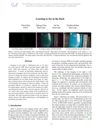
Transcription
MICHIGAN STATE UNIVERSITY COLLEGE OF ENGINEERINGDesign a Single-layer PCBUsing EagleECE480 Senior Design Team 5Cheng Zhang11/15/2012Abstraction: This application note is a tutorial of designing a single-layer PCB using Eagle program. Thetutorial will guild the reader through building schematic, designing PCB layout and generating CAM filesin the Eagle program.
Design Single-Layer PCB Using EagleContentsIntroduction . 2Objective . 2Getting started with schematic. 2From schematic to layout . 10Preparing for fabrication with CAM . 121
Design Single-Layer PCB Using EagleIntroductionPCB, which is also known as printed circuit board, is very commonly used incommercially produced electronic devices. A printed circuit board usually use conductivepathways, tracks and traces etched or striped from a copper sheet covered on a non-conductivesubstrate. PCB is also a very reliable and a very effective way of implementing a designed circuitwith a good manufacturability.To design a PCB from a circuit schematic usually involves computer aided designsoftware. In this application notes, Eagle program which is developed by Cadsoft will beintroduced. This tutorial will walk the reader through building the schematic in Eagle anddesigning the layout of the PCB. Eagle, stands for easily applicable graphical layout editor, iscapable of schematic capture, PCB layout, and CAM. In this tutorial, every feature will bediscussed respectively.There are a few visions of Eagle for different tasks. The one that will be used in thistutorial is a free version of Eagle. The free version of Eagle is restricted to a maximum size of3.9 inches by 3.2 inches. It is capable of designing two-layer PCB, while this tutorial will onlydemonstrate the single-layer PCB layout. Even with the restrictions, the free version of Eagle isstill an ideal tool of design small single-layer printed circuit board.A free version of Eagle is available for downloading through the following guage enObjectiveThe objective of this tutorial is to help readers to design a printed circuit board from aschematic. The tutorial also includes techniques such as CAM process, which are both veryuseful and necessary steps for building a printed circuit board.Key words: Single-layer PCB, layout, CAM, schematic, Eagle, CadsoftGetting Started with SchematicIn this tutorial, the following example will be used as demonstration. This demonstrationinvolves some representative elements to be introduced. Readers should find it helpful by followthe steps respectively.2
Design Single-Layer PCB Using EagleFirst of all, run Eagle program. The Control Panel will be displayed. On the Control Panel, selectFile New Schematic. That will open a new schematic window. On the left of the schematicwindow, there is a add tool:This Add tool will add elements such as resistor, capacitor and ICs, all of which are veryimportant in designing the PCB.3
Design Single-Layer PCB Using EagleOnce the add tool is select, it will open a window:On this window, a proper element needs to be selected. The Add tool serves like a library ofelements. There are a lot of elements manufactured by different companies to be chosen from.However, this library may not contain all the elements needed for project. It is possible thatcertain project needs to use an element that is not contained in the library. In that case, there aredifferent element libraries online for Eagle to use. User need to find the proper library to do theirproject. In the demonstration, LM324N will be used to show how a chip will be added.To find LM324N in the library, search for “LM324N”:4
Design Single-Layer PCB Using EagleTips: ICs like LM324 are usually contained in the library. However, due to different packageof the ICs, the package information must be included in the key words. In this case, instead ofsearching LM324, searching LM324N will return the correct element.The particular LM324N used in the demonstration has four op-amps built-in in a single chip. Thechip has a DIL14 package which stands for dual in line package. This is a standard through-holepackage for LM324. To add LM324 to the schematic, press OK and place two op-amps on theschematic. Eagle will automatically use two op-amps within the total of four, respectively, thefirst two op-amps on the chip. Now the schematic should look like:5
Design Single-Layer PCB Using EagleThen, resistors need to be added. Select Add tool again and search for resistor. Use the key word“resistor”. That should return a lot of results. The choice of resistor completely depends on thesize of the resistor. In this demonstration, the resistor with grid of 10mm is chosen for this demo.Then press OK and place five resistors on the schematic. Then wires need to be added to connectthe elements. To add wires, select wire on the left of the window:6
Design Single-Layer PCB Using EagleThen, click on any spot wished and that will be the start point of a wire. Click again will be placea turning point of the wire. Notice that it is not the end point. To end a segment of wire, pressEsc. Then, connect the element according to the schematic:7
Design Single-Layer PCB Using EagleTo finish the schematic, a potentiometer needs to be added. To add a potentiometer takes somemore efforts to find. In this demonstration, a potentiometer manufactured by Spectrol is used.This particular potentiometer has a square package and the three pins are in a line. Search forpotentiometer. This particular potentiometer is in the directory of TRIM RE. Expand thedirectory and find the particular potentiometer manufactured by Spectrol:Click OK and place the potentiometer where it should be. Then connect the potentiometer to thecircuit. Then, ground needs to be added to the schematic. To add ground, select add tool againand search for GND. Then choose either one from the two ground symbol available and placeground where it needs to be:8
Design Single-Layer PCB Using EagleThen, connect the ground as shown in the circuit schematic. The last task is to add two solderingpad for input and output of the circuit. Open the add tool again and search for “solder”. There areseveral kinds of soldering pads to choose from. In this turtorail, a soldering pad of 1mm diameterwill be chosen:9
Design Single-Layer PCB Using EagleThen connect the soldering pad to the circuit, the schematic of the circuit is finished then:From Schematic to LayoutAfter the schematic is done, press the bottom shown in the picture:10
Design Single-Layer PCB Using EagleThis will automatically open a PCB board window and have the elements and signal wires inplace:Then, move the element to the designated board area and adjust them so that traces can be runbetween elements without crossover:Then click the wire bottom in the picture to wire the traces according to the signal wires on theboard. Once the traces are run from a point to another, the signal wires originally on it will beautomatically removed indicates that the signal has been completed.The finished traces should look something like this:11
Design Single-Layer PCB Using EagleThere are two things to be noticed. First, in the program, because the LM324N was addedwithout power supply pin, the power supply of the chip needs to be added afterwards. Thus, copyand paste a soldering pad as the VCC connector. Then connect the soldering pad to pin 5 ofLM324N. Second, the ground was automatically connected to the ground plate. However, thepurpose of this tutorial is to show how to design a single layer PCB which doesn’t provide aground plate. In this case, record the connections to be grounded and solder the connections tothe copper plate and the copper plate will serve as the ground.The finished PCB layout will look like:Preparing for Fabrication with CAMOn the Control Panel, choose gerb274xECESHOP from the drop-down list of the CAM Jobs:12
Design Single-Layer PCB Using EagleThat will open a window. Select File Open Board. Choose the board to be fabricated and clickOK. Then on the following screen, click Process Job:Five Gerber files will be generated in the same directory in which the board file is. They shouldhave extensions of .bol .cmp, .gbr, .gpi and .sol. The five files are what is needed for the PCB tobe fabricated.13
Design Single-Layer PCB Using EagleConclusionAfter read the tutorial, the readers should know how to create a schematic for the PCB to befabricated, transform the schematic into a PCB layout and generate the CAM files necessary forfabrication. Though the demonstration and the intension of the tutorial is to build a single-layerPCB, the techniques are very similar when readers moving to multiple-layer PCBs.14
In this tutorial, every feature will be discussed respectively. There are a few visions of Eagle for different tasks. The one that will be used in this tutorial is a free version of Eagle. The free version of Eagle is restricted to a maximum size of 3.9 inches by 3.2 inches. It is capable of designing two-layer PCB, while this tutorial will only