Transcription
4H- and 6H- Silicon Carbide in PowerMOSFET DesignByMd HasanuzzamanDepartment of Electrical & Computer EngineeringThe University of Tennessee, KnoxvilleApril 7, 20041Analog VLSI andDevices Laboratory
Agenda¾¾¾¾¾¾¾Overview of silicon carbideComparison of Si and SiC MOSFETVertical power MOSFET modelA proposed device structureMOSFET temperature modelResultsConclusions2Analog VLSI andDevices Laboratory
Why SiC?¾Large band gap and high meltingpoint enable high temperature deviceoperations¾Large break down field enable thefabrication of smaller and compacthigh voltage power devices¾Requires smaller cooling system dueto High thermal conductivity¾Extremely radiation hard¾Shows excellent reverse recoverycharacteristics¾Excellent mechanical propertiesmake SiC ideal for MEMS applications3High breakdownelectric fieldHigh thermalconductivityHigh power hightemperature deviceWidebandgapHigh currentdensityRadiationhardAnalog VLSI andDevices Laboratory
Why Not Silicon?¾Smaller band gap and lowmelting point enable mediumrange of temperature deviceoperations¾Due to lower thermalconductivity, requires largercooling system¾Smaller electric breakdownfield limit the device size andvoltage¾Shows high leakage currentOn-ResistanceSiCSiBreakdown VoltageElectric FieldThermalConductivityFig: Comparison of Si and SiC properties4Analog VLSI andDevices Laboratory
Physical & Electrical Properties of SiCPropertiesSi6H-SiC4H-SiCBandgap(eV )1.113.03.26Dielectric const.11.89.710Breakdown field(V/cm)6x1053.5x1063.5x106Saturated drift velocity(cm/sec)1x1072x1072x107Electron mobility(in bulk) (cm2/V-sec)1350370720a650c450951201.54.94.9Melting point (oC)142028302830Hardness (kg/mm2)1000-2310Hole mobility (inbulk) (cm2/V-sec)Thermal conductivity(W/cm-oK)a along a-axis, c along c-axis5Analog VLSI andDevices Laboratory
Comparison of Wide Bandgap MaterialsProperties¾SiC is unique because of itsnative oxide is SiO2 ,therefore easy to fabricatefield effect device¾Though Diamond has thebest material properties, it isnot suitable for conventionalelectronic device fabrication.¾It is very difficult to formoxide in GaN, it is suitable foropto-electronics devices64H-SiCGaNDiamondLattice constant (Å)3.073 a10.053 c4.513.57Thermal expansion (x10-6)oC-5.60.08Density (g/cm3)--3.51Melting point (oC)2830-4000Bandgap (eV)3.263.455.45Saturated electronvelocity (x107 cm/s)2.02.22.7Mobility (cm2/V-s)ElectronHoleBreakdown Voltage (x105V/cm)78050301250250 5022001600100Dielectric constant9.66115.5Resistivity (Ω-cm)-10101013Thermal conductivity(W/cm.K)4.91.320Hardness (kg/mm2)2130 a-10000Analog VLSI andDevices Laboratory
Power MOSFET design considerations¾Specific on-resistance has to bekept as low as possible¾Breakdown voltage has to increaseas design requirements¾Low specific on-resistance reducespower losses and increases efficiency¾Specific on-resistance increaseswith the increase of the breakdownvoltage¾A design trade-off has to be madebetween the specific on-resistanceand the voltage rating7VBr Ron spε .Ec22.q.N d4VBr2 ε .E c3 .µ nGSSOxiden RCHChannelRCHp-bodyp-bodyRD4H-SiC n- driftregionn DAnalog VLSI andDevices Laboratory
Power MOSFET design considerations (contd.)¾SiC devices demonstrate onehundredth times lower specific onresistance and ten times higherbreakdown voltage than the silicondevices for the same device dimensions¾Drift region thickness is ten timeslower in silicon carbide compared tosilicon device for same voltage rating¾Mass and volume of heat sink is 1520% smaller in case of silicon carbideWdrift 2VBrEcGSSOxiden RCHChannelRCHp-bodyp-body4H-SiC n- driftregionRDn D8Analog VLSI andDevices Laboratory
Comparison of Si & SiC Power MOSFETsGGSSSOxiden RCHSOxiden RCHChannelRCHp-bodyChannelRCHp-bodyn p-bodyp-bodyRDRD4H-SiC n- driftregionn n- driftregionDn DSi-MOSFETSiC-MOSFET & Heat sinkSiliconSilicon-Carbide100 m.Ω/cm21 m.Ω/cm2Drift Region Thickness100 µm10 µmOperating Temperature150oC500oCHeat Sink Volume & Mass100%80-85%Device size100%50%On-Resistance9Heat sink for Si devicesAnalog VLSI andDevices Laboratory
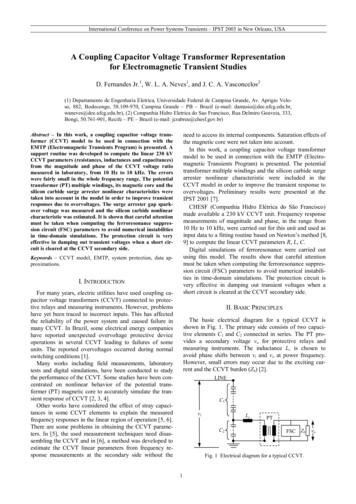
Future power electronics will be SiC !Today’sTechnologyAdvantages ofSilicon CarbideLarge energy lossesReduce loss by 10xLarge improvement inefficiencyLimited voltage andpower levelIncrease power 103xSimplify use in electricalgridLow operatingtemperature ( 150ºC)Increase range to 500ºCNew applications;eliminate massive heatsinksLarge heat sinks & filtersReduce size/weightby 3xLightweight, compactsystems10PayoffAnalog VLSI andDevices Laboratory
Potential applications of SiC ar power11AircraftAnalog VLSI andDevices Laboratory
Limitations of SiC¾Higher defect densities due tomicropipes and dislocations in thecrystal orientations¾Material processing and devicefabrication require hightemperature process (1000-1700oC)¾Device quality SiC wafer is verycostly¾High interface state densities¾Low inversion layer mobility¾Power MOSFETs in SiC are notcommercially availableMicropipes defects2.540DS 50 mV352W et NO30251.520115100.5Dry W et0051015205Mobility (cm2/Vs)Drain Current (µA)V025Gate Voltage (V)12Analog VLSI andDevices Laboratory
Atomic structure¾SiC are made bySiarrangement of covalentlybonded tetrahedral Si and CatomsCTetragonal bonding betweencarbon and silicon atoms¾50% carbon atoms and 50Locations of Si (light) and Catoms (dark) in SiC% silicon atoms¾SiC has more than 100Bknown polytypesA¾Polytype refers to a familyof material which hascommon stoichiometriciti b t tCSite locations for C atoms in (0001) plan13Analog VLSI andDevices Laboratory
Atomic structure (contd.)¾The arrangement of SiC bi-layersis same in 2-D but differs in bystacking sequence in 3-D¾3 commonly used polytypes:AB¾ 3C-SiC: Cubic structure, Zincblend, ABCABC .¾ 4H-SiC: Hexagonal closepacked, ABCBABCB ¾ 6H-SiC: Hexagonal closepacked, ABCACBABCAC ACBA3CACBACACCBBBBAAAA2H4H6HStacking sequences for four different SiC polytypes14Analog VLSI andDevices Laboratory
Device fabrication:the pathway to success¾Material Processing Epitaxial Growth Dopant Activation Interface EngineeringM aterialProcessing¾Device Fabrication¾Applications Circuit Design System IntegrationD eviceFabricationDesignFlowP otentialA pplications15Analog VLSI andDevices Laboratory
Drawback of lateral structure for power application¾ PowerMOSFETs have to handlehigh voltages and high currents¾Lateral structure is not suitable forpower application¾ Current flows laterally through thechannel below the gate oxide¾ No drift region available to holdlarge voltage¾ No option is available for forwardblocking capability¾ Required large W to get large W/Lratio to increase the current capacitySGDOXIDEn Channeln p-type substrateBLateral MOSFET Structure16Analog VLSI andDevices Laboratory
Vertical MOSFET for high voltage and high power¾Source and drain are made on top andbottom of the wafer respectivelyG¾ Current flows vertically from drain tosource through drift and channel regionSSOxiden Channelp-body¾ Drift region supports most of theapplied drain voltage¾Channel region provides the currentp-body4H-SiC n- driftregiongainn ¾ p-n junction between p-body and n-drift region provides forward blockingcapability17DVertical MOSFET StructureAnalog VLSI andDevices Laboratory
Vertical MOSFET for high voltage and high power¾P-bodies can be made either round orhexagonal shaped to get large WGS¾Length L can be made very smallSOxide¾For same die area, W/L ratio is highercompared to lateral MOSFET¾Drift region doping can be adjusted toget high breakdown voltage with low onresistancen Channelp-bodyp-body4H-SiC n- driftregionn ¾4H-SiC is suitable for vertical structuredue to higher mobility in verticaldirectionD18Analog VLSI andDevices Laboratory
Modeling of vertical DIMOS structure¾For analysis the structure is dividedinto two regions: (i) the channel region,and (ii) the drift region¾ Channel forms in the p-body belowthe gate oxide where gate voltagecontrols the channel currents¾ Drain current is divided into twochannel currents in two p-bodies on bothsides¾ Drift region begins at the drain andends at the channel near the oxide layerLGLpSSOxiden p-bodyRegion An p-bodyLsRegion BWjWdαWtRegion Cn DCross-section details of VDIMOSstructure used in the modelM Hasanuzzaman, S.K. Islam, L. Tolbert, and Burak Ozpineci,“Model Simulation and Verification of a VerticalDouble Implanted (DIMOS) Transistor in 4H-SiC”, proceedings of the IASTED international conference,February 24-26, 2003, Palm Spring, CA.19Analog VLSI andDevices Laboratory
Modeling of vertical DIMOS structure (contd.)¾Drift region is divided into threeregions¾ Region A: an accumulation regionbetween the p-bodies with smallcross-section¾ Region B: a drift region withvarying cross-section¾ Region C: a drift region withconstant cross-section¾ Current voltage relations forchannel region and three drift regionshave been developed20LGLpSSOxiden p-bodyRegion An p-bodyLsRegion BWdαWjWtRegion Cn DAnalog VLSI andDevices Laboratory
Modeling of vertical DIMOS structure (contd.)Channel CurrentI ch [Wµ neff2 L 1 ( µ neff / 2vsat L)VchVch [2Cox (VGS VT ) (Cox Cdo )Vch ]]LGLpSCox Cdo is the totalcapacitance of the oxide and the bodydepletionS¾ Where¾ Current increases with the decrease ofchannel length and increase in channelwidth and voltageOxiden p-bodyRegion An p-bodyLsRegion BWdαWjWtRegion Cn ¾ Gate voltage controls the channelcurrentD¾ At saturation, channel current is givenby,I ch ( sat ) Wvsat Cox (VGS VT )21Analog VLSI andDevices Laboratory
Modeling of vertical DIMOS structure (contd.)Drift Region VoltageTotal drift region voltage is thesum of the voltages of the threeregions,Vdrift VA VB VCWhere,LGSSOxiden p-bodyRegion AVA E y dy 0I D (W j W d )W ( L s qN d µ n ) I D / E C WqNd µ n (Ls 2LP ) I D / EC VB log WqNd µ n cotαWqNd Ls µ n I D / EC n p-bodyLsRegion BW j W dLpWdαWjWtRegion Cn IDVC DI D (Wt W j Wd LP tan α )WqN d µ n ( LS 2 LP ) I D Ec22Analog VLSI andDevices Laboratory
Results from the analytical model¾Voltage and current equations areµn-SiC 40 cm2/V.s,solved numerically because of theimplicit nature of the two sets ofequationstox 500 Åεox 3.9x8.854x10-12 F/cm¾ The parameter values of 4H-SiCare used to evaluate the drain currents¾ A number of output characteristicsare obtained for different gatevoltagesL 1 µm,Wt 25 µmLp 15 µm, Wj 5 µmLs 18 µmOutput Characteristics of vertical DIMOS with4H-SiC parametersVT 1V23Analog VLSI andDevices Laboratory
Results of analytical model(contd.)¾ Effectsof impurity concentrationsof drift region and narrow p-bodyspacing regions have been observedTransfer characteristic of Vertical DMOSfor different temperature¾ Gate loses its control over the draincurrent if velocity saturation occursbefore the drain pinches offDrain currents (Amp)1¾ Larger p-body separation reducesthe quasi-saturation effect0.75T 400oKoT 300 K0.5T 500oK0.25Crossover0¾ Lower impurity concentrations010203040Gate voltage (volts)increase the quasi-saturation effectTransfer Characteristics of VDIMOS with4H-SiC parameters¾ Transfer characteristics show aclear crossover with temperaturevariation at a gate voltage of 15V24Analog VLSI andDevices Laboratory
Model verification using ATLAS simulations¾Vertical MOSFET structure in 4H-SiC is proposed to verify the analyticalmodel¾ n-Drift is doped lightly (4.2x1015cm3) to hold the desired breakdownvoltage¾ n regions are doped (1.5x1020cm-3) with Nitrogen¾ p-body is formed by Aluminumimplantations (4x1017cm-3)¾ p-bodies are separated by 20µm¾ Oxide thickness is 500ž Drift region thickness is 20µm25GSSOxiden Channelp-bodyp-body4H-SiC n- driftregionn DVertical MOSFET Structure in 4H-SiCAnalog VLSI andDevices Laboratory
Device dimensions for the proposed 4H-SiC DIMOSDevice dimensionsDopingRegionDoping levelImpurityChannel width400 µmn-drift4x1015cm-3NitrogenChannel length1 µmp-bodies4x1017cm-3AluminumOxide thickness500 Ån region(1.5x1020cm-3)Nitrogenp-bodies separation20 µmEpilayer thickness25 µm26Analog VLSI andDevices Laboratory
Simulation results using ATLAS device simulatorDrain currentsAnalytical modelATLAS simulations220 mA at VGS 10V232 mA at VGS 10V54 mΩ.cm260 mΩ.cm22.6kV2.3kVSpecific on-resistanceBreakdown voltageOutput characteristics from ATLAS simulatorBreakdown voltage variation with gate length27Analog VLSI andDevices Laboratory
Simulation results using ATLAS device simulator (contd.)¾Optimum gate width of 20 µm is obtained for minimum specific on-resistance¾ A good agreement between the theoretical and the simulated values of breakdown voltage¾ Specific on-resistance values are in the same magnitude compared to the recently published values¾ Clear quasi-saturation effect has been observed in ATLAS simulation¾ Good agreement between the analytical model and the proposed device structureComparison of theoretical and simulated values of breakdown voltageswith drift layer thickness as a parameter28Variation of specific on-resistance with gate widthAnalog VLSI andDevices Laboratory
Temperature modeling for lateral MOSFET¾ID MOSFET channel current, atroom temperature¾IR Body leakage currentD¾ITH Current change due to thethreshold voltage changeItotalID¾IRDS Current change due to thechange of drain and source contactregion resistanceIRGITHIRDS¾ID is kept constant over thetemperature variation¾The compensating currents incorporatethe change in the MOSFET's currentSMOSFET model with temperature compensation*M. Hasanuzzaman, S.K. Islam and L.M. Tolbert, “Effects of temperature variation (300o-600o K) inMOSFET modeling in 6H silicon carbide”, Solid State Electronics, Vol 48/1 pp 125-132, 200429Analog VLSI andDevices Laboratory
Temperature modeling for lateral MOSFET(contd.)Total Drain CurrentI total I D I R I TH I RDSDWhere,ID ItotalWµ n C ox [(VGS VTH ) VDS / 2]VDSLID Eg Dn ni23I R qAαAT exp Ln N A kT IRGW′ VTH ]VDSµ nCox [VTHL 11 VDS β ' RDS RDS ITHIRDSI TH I RDSSMOSFET model with temperature compensation30Analog VLSI andDevices Laboratory
Results of temperature model in 6H-SiC¾ The model simulations match perfectly with the measured data at 300oK¾ The simulations at 600oK match reasonably with the measured data with minor discrepancies¾At 300oK, the drain current is 15µA, whereas it rises to 235µA at 600oK for a gate voltageVGS 6V3002018simulatedo x* measured250Vgs 6V14Drain Currents ( µA)Drain Currents ( µA)1612108Vgs 5V64Vgs 6V200150Vgs 5V100Vgs 4V50Vgs 3VVgs 4V200simulatedo x* measured2Vgs 3V468Drain-Source Voltage (volts)0010Output characteristics for simulated and measured data at300oK2468Drain-Source Voltage (volts)10Output characteristics for simulated and measured data at600oK31Analog VLSI andDevices Laboratory
Results of temperature model in 6H-SiC (contd.)Contribution of the compensating currents to the total current changeTemperature(oK)Total Currentchange (µA)Due to ITHDue to IRDue to - simulated at Vds 5v--- simulated at Vds 5vDrain Currents (µA)Drain Currents (µA)20010515010050001234Gate to Source Voltage (volts)5006Transfer characteristics simulated at drain-source voltage VDS 5V,temperature 300oK3212345Gate to Source Voltage (volts)6Transfer characteristics simulated at drain-source voltageVDS 5V, temperature 600oKAnalog VLSI andDevices Laboratory
Results of temperature model in 4H- & 6H-SiC¾Drain currents of 6H-SiC MOSFET are greater than their 4H-SiC counterparts by a factor ofapproximately 2.5¾ Higher mobility of 6H-SiC ( 100 cm2/V.sec) results in higher drain current of 6H-SiC MOSFETcompared to 4H-SiC MOSFETs¾ Simulation results show a better performance for 6H-SiC MOSFETs25018Dotted line: 4H-SiC16 Solid line : 6H-SiC200Drain Currents (µA)Drain Currents ( µA)1412Vgs 6V1086Vgs 5V4Dotted line: 4H-SiCSolid line : 6H-SiC150o600 K10050200o300 KVgs 4V2468Drain-Source Voltage (volts)0010Output characteristics of 4H- & 6H-SiC lateral MOSFET at300oK12345Gate to Source Voltage (Volts)6Transfer characteristics of 4H- & 6H-SiC lateral MOSFET*M. Hasanuzzaman, S.K. Islam and L.M. Tolbert, “Temperature Dependency of MOSFET DeviceCharacteristics in 4H- and 6H-Silicon Carbide (SiC)” ”, to be presented in ISDRS’2003Analog VLSI and33Devices Laboratory
Results of temperature model in 4H- & 6H-SiC¾Threshold voltage changes from 3.2V at 300oK to 1.2V at 600oK¾Simulated values of the threshold voltages matches with the measured data¾Variation of threshold voltage for 4H-SiC is predicted using the model3.53.5simulatedo measured3Threshold Voltage (volts)Threshold Voltage 0Temperature(oK)5500.5300600Threshold voltages obtained from simulation and measurement fordifferent old voltage variation of 4H- & 6H-SiC lateral MOSFETwith temperature34Analog VLSI andDevices Laboratory
Conclusions¾ Silicon carbide is better alternate material for high power andhigh temperature device application¾ An analytical model for vertical DIMOS in 4H-SiC is developed¾ A device structure is proposed to verify the model¾ A temperature model for lateral MOSFET is developed¾ Simulation with MOSFET temperature model is carried out for4H- and 6H-SiC materials35Analog VLSI andDevices Laboratory
Thanks!!36Analog VLSI andDevices Laboratory
6 Analog VLSI and Devices Laboratory Comparison of Wide Bandgap Materials Properties 4H-SiC GaN Diamond Lattice constant (Å) 3.073 a 10.053 c 4.51 3.57 Thermal expansion (x10-6) oC - 5.6 0.08
