Transcription
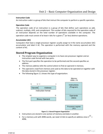
Unit 2 – Basic Computer Organization and DesignInstruction CodeAn instruction code is a group of bits that instruct the computer to perform a specific operation.Operation CodeThe operation code of an instruction is a group of bits that define such operations as add,subtract, multiply, shift, and complement. The number of bits required for the operation code ofan instruction depends on the total number of operations available in the computer. Thenoperation code must consist of at least n bits for a given 2 (or less) distinct operations.Accumulator (AC)Computers that have a single-processor register usually assign to it the name accumulator (AC)accumulator and label it AC. The operation is performed with the memory operand and thecontent of AC.Stored Program Organization The simplest way to organize a computer is to have one processor register and aninstruction code format with two parts. The first part specifies the operation to be performed and the second specifies anaddress. The memory address tells the control where to find an operand in memory. This operand is read from memory and used as the data to be operated on together withthe data stored in the processor register. The following figure 2.1 shows this type of organization. Figure 2.1: Stored Program Organization Instructions are stored in one section of memory and data in another. 12For a memory unit with 4096 words, we need 12 bits to specify an address since 2 4096. 1 PageUNIT-II
Unit 2 – Basic Computer Organization and Design If we store each instruction code in one 16-bit memory word, we have available four bitsfor operation code (abbreviated opcode) to specify one out of 16 possible operations,and 12 bits to specify the address of an operand. The control reads a 16-bit instruction from the program portion of memory. It uses the 12-bit address part of the instruction to read a 16-bit operand from the dataportion of memory. It then executes the operation specified by the operation code. Computers that have a single-processor register usually assign to it the nameaccumulator and label it AC. If an operation in an instruction code does not need an operand from memory, the restof the bits in the instruction can be used for other purposes. For example, operations such as clear AC, complement AC, and increment AC operate ondata stored in the AC register. They do not need an operand from memory. For thesetypes of operations, the second part of the instruction code (bits 0 through 11) is notneeded for specifying a memory address and can be used to specify other operations forthe computer. Direct and Indirect addressing of basic computer. The second part of an instruction format specifies the address of an operand, theinstruction is said to have a direct address. In Indirect address, the bits in the second part of the instruction designate an address ofa memory word in which the address of the operand is found. One bit of the instruction code can be used to distinguish between a direct and anindirect address. It consists of a 3-bit operation code, a 12-bit address, and an indirect address mode bitdesignated by I. The mode bit is 0 for a direct address and 1 for an indirect address. A direct address instruction is shown in Figure 2.2. It is placed in address 22 in memory. The I bit is 0, so the instruction is recognized as a direct address instruction. The opcode specifies an ADD instruction, and the address part is the binary equivalent of457. The control finds the operand in memory at address 457 and adds it to the content ofAC. The instruction in address 35 shown in Figure 2.3 has a mode bit I 1, recognized as anindirect address instruction. The address part is the binary equivalent of 300. The control goes to address 300 to find the address of the operand. The address of theoperand in this case is 1350. The operand found in address 1350 is then added to thecontent of AC. 2 PageUNIT-II
Unit 2 – Basic Computer Organization and Design The indirect address instruction needs two references to memory to fetch an operand. 1. The first reference is needed to read the address of the operand2. Second reference is for the operand itself.The memory word that holds the address of the operand in an indirect addressinstruction is used as a pointer to an array of data. 15I1412 11Opcode0AddressMemory224570 ADDMemory45735 1 ADD30030013501350OperandOperand ACACFigure 2.2: Direct AddressDirect AddressWhen the second part of aninstruction code specifies the addressof an operand, the instruction is saidto have a direct address.For instance the instruction MOV R000H. R0, when converted to machinelanguage is the physical address ofregister R0. The instruction moves 0to R0.Figure 2.3: Indirect AddressIndirect AddressWhen the second part of an instructioncode specifies the address of a memoryword in which the address of the operand,the instruction is said to have a directaddress.For instance the instruction MOV @R0 00H,when converted to machine language, @R0becomes whatever is stored in R0, and thatis the address used to move 0 to. It can bewhatever is stored in R0.3 PageUNIT-II
Unit 2 – Basic Computer Organization and DesignRegisters of basic computer It is necessary to provide a register in the control unit for storing the instruction codeafter it is read from memory. The computer needs processor registers for manipulating data and a register for holdinga memory address. These requirements dictate the register configuration shown in Figure 2.4. Figure 2.4: Basic Computer Register and Memory The data register (DR) holds the operand read from memory. The accumulator (AC) register is a general purpose processing register. The instruction read from memory is placed in the instruction register (IR). The temporary register (TR) is used for holding temporary data during the processing. The memory address register (AR) has 12 bits. The program counter (PC) also has 12 bits and it holds the address of the next instructionto be read from memory after the current instruction is executed. Instruction words are read and executed in sequence unless a branch instruction isencountered. A branch instruction calls for a transfer to a nonconsecutive instruction inthe program. Two registers are used for input and output. The input register (INPR) receives an 8-bitcharacter from an input device. The output register (OUTR) holds an 8-bit character foran output device. 4 PageUNIT-II
Unit 2 – Basic Computer Organization and er NameFunction16121616121688Data registerAddress registerAccumulatorInstruction registerProgram counterTemporary registerInput registerOutput registerHolds memory operandHolds address for memoryProcessor registerHolds instruction codeHolds address of instructionHolds temporary dataHolds input characterHolds output characterTable 2.1: List of Registers for Basic ComputerCommon Bus System for basic computer register. What is the requirement of common bus System? The basic computer has eight registers, a memory unit and a control unit. Paths must be provided to transfer information from one register to another andbetween memory and register. The number of wires will be excessive if connections are between the outputs of eachregister and the inputs of the other registers. An efficient scheme for transferringinformation in a system with many register is to use a common bus. The connection of the registers and memory of the basic computer to a common bussystem is shown in figure 2.5. The outputs of seven registers and memory are connected to the common bus. Thespecific output that is selected for the bus lines at any given time is determined from thebinary value of the selection variables S2, S1, and S0. The number along each output shows the decimal equivalent of the required binaryselection. The particular register whose LD (load) input is enabled receives the data from the busduring the next clock pulse transition. The memory receives the contents of the buswhen its write input is activated. The memory places its 16-bit output onto the bus whenthe read input is activated and S2 S1 S0 1 1 1. Four registers, DR, AC, IR, and TR have 16 bits each. Two registers, AR and PC, have 12 bits each since they hold a memory address. When the contents of AR or PC are applied to the 16-bit common bus, the four mostsignificant bits are set to 0’s. When AR and PC receive information from the bus, only the 12 least significant bits are transferred into the register. The input register INPR and the output register OUTR have 8 bits each and communicatewith the eight least significant bits in the bus. INPR is connected to provide informationto the bus but OUTR can only receive information from the bus. 5 PageUNIT-II
Unit 2 – Basic Computer Organization and DesignFigure 2.5: Basic computer registers connected to a common bus Five registers have three control inputs: LD (load), INR (increment), and CLR (clear). Tworegisters have only a LD input. AR must always be used to specify a memory address; therefore memory address isconnected to AR. The 16 inputs of AC come from an adder and logic circuit. This circuit has three sets ofinputs. 1. Set of 16-bit inputs come from the outputs of AC.2. Set of 16-bits come from the data register DR.3. Set of 8-bit inputs come from the input register INPR.The result of an addition is transferred to AC and the end carry-out of the addition istransferred to flip-flop E (extended AC bit). The clock transition at the end of the cycle transfers the content of the bus into thedesignated destination register and the output of the adder and logic circuit into AC. 6 PageUNIT-II
Unit 2 – Basic Computer Organization and DesignInstruction Format with its types. The basic computer has three instruction code formats, as shown in figure 2.6. Figure 2.6: Basic computer instruction format Each format has 16 bits. The operation code (opcode) part of the instruction contains three bits and the meaningof the remaining 13 bits depends on the operation code encountered. A memory-reference instruction uses 12 bits to specify an address and one bit to specifythe addressing mode I. I is equal to 0 for direct address and to 1 for indirect address. The register reference instructions are recognized by the operation code 111 with a 0 inthe leftmost bit (bit 15) of the instruction. A register-reference instruction specifies anoperation on or a test of the AC register. An operand from memory is not needed;therefore, the other 12 bits are used to specify the operation or test to be executed. An input-output instruction does not need a reference to memory and is recognized bythe operation code 111 with a 1 in the leftmost bit of the instruction. The remaining 12bits are used to specify the type of input-output operation or test performed. Control Unit with timing diagram. The block diagram of the control unit is shown in figure 2.7. Components of Control unit are 1. Two decoders2. A sequence counter3. Control logic gates An instruction read from memory is placed in the instruction register (IR). In control unitthe IR is divided into three parts: I bit, the operation code (12-14)bit, and bits 0 through11. The operation code in bits 12 through 14 are decoded with a 3 X 8 decoder. 7 PageUNIT-II
Unit 2 – Basic Computer Organization and DesignFigure 2.7: Control unit of basic computer Bit-15 of the instruction is transferred to a flip-flop designated by the symbol I. The eight outputs of the decoder are designated by the symbols D0 through D7. Bits 0through 11 are applied to the control logic gates. The 4‐bit sequence counter can countin binary from 0 through 15.The outputs of counter are decoded into 16 timing signals T0through T15. The sequence counter SC can be incremented or cleared synchronously. Most of thetime, the counter is incremented to provide the sequence of timing signals out of 4 X 16decoder. Once in awhile, the counter is cleared to 0, causing the next timing signal to beT0. As an example, consider the case where SC is incremented to provide timing signals T0,T1, T2, T3 and T4 in sequence. At time T4, SC is cleared to 0 if decoder output D3 is active.This is expressed symbolically by the statement D3T4: SC 0Timing Diagram: The timing diagram figure2.8 shows the time relationship of the control signals. The sequence counter SC responds to the positive transition of the clock. Initially, the CLR input of SC is active. The first positive transition of the clock clears SC to 0, which in turn activates the timingT0 out of the decoder. T0 is active during one clock cycle. The positive clock transition 8 PageUNIT-II
Unit 2 – Basic Computer Organization and Design labeled T0 in the diagram will trigger only those registers whose control inputs areconnected to timing signal T0.SC is incremented with every positive clock transition, unless its CLR input is active. This procedures the sequence of timing signals T0, T1, T2, T3 and T4, and so on. If SC is notcleared, the timing signals will continue with T5, T6, up to T15 and back to T0. T0T1T2T3T4T0ClockT0T1T2T3T4D3CLR SCFigure 2.8: Example of control timing signals The last three waveforms shows how SC is cleared when D3T4 1. Output D3 from theoperation decoder becomes active at the end of timing signal T 2. When timing signal T4becomes active, the output of the AND gate that implements the control function D 3T4becomes active. This signal is applied to the CLR input of SC. On the next positive clock transition thecounter is cleared to 0. This causes the timing signal T 0 to become active instead of T5that would have been active if SC were incremented instead of cleared. 9 PageUNIT-II
Unit 2 – Basic Computer Organization and DesignInstruction cycle A program residing in the memory unit of the computer consists of a sequence ofinstructions. In the basic computer each instruction cycle consists of the followingphases: 1. Fetch an instruction from memory.2. Decode the instruction.3. Read the effective address from memory if the instruction has an indirect address.4. Execute the instruction.After step 4, the control goes back to step 1 to fetch, decode and execute the nexinstruction. This process continues unless a HALT instruction is encountered. Figure 2.9: Flowchart for instruction cycle (initial configuration) The flowchart presents an initial configuration for the instruction cycle and shows howthe control determines the instruction type after the decoding. If D7 1, the instruction must be register-reference or input-output type. If D7 0, theoperation code must be one of the other seven values 110, specifying a memoryreference instruction. Control then inspects the value of the first bit of the instruction,which now available in flip-flop I. If D7 0 and I 1, we have a memory-reference instruction with an indirect address. It isthen necessary to read the effective address from memory. The three instruction types are subdivided into four separate paths. The selected 10 P a g eUNIT-II
Unit 2 – Basic Computer Organization and Designoperation is activated with the clock transition associated with timing signal T3.This canbe symbolized as follows:D’7 I T3: AR M [AR]D’7 I’ T3: NothingD7 I’ T3: Execute a register-reference instructionD7 I T3: Execute an input-output instructionWhen a memory-reference instruction with I 0 is encountered, it is not necessary to doanything since the effective address is already in AR. However, the sequence counter SC must be incremented when D’7 I T3 1, so that theexecution of the memory-reference instruction can be continued with timing variable T4. A register-reference or input-output instruction can be executed with the clickassociated with timing signal T3. After the instruction is executed, SC is cleared to 0 andcontrol returns to the fetch phase with T0 1. SC is either incremented or cleared to 0with every positive clock transition. Register reference instruction. When the register-reference instruction is decoded, D7 bit is set to 1. Each control function needs the Boolean relation D7 I' T3 150 1 1 1 12 110Register OperationThere are 12 register-reference instructions listed below: SC 0r:AC 0CLArB11:E 0CLErB10:AC AC’CMArB9:E E’CMErB8:AC shr AC, AC(15) E, E AC(0)CIRrB7:AC shl AC, AC(0) E, E AC(15)CILrB6:AC AC 1INCrB5:if (AC(15) 0) then (PC PC 1)SPArB4:if (AC(15) 1) then (PC PC 1SNArB3:if (AC 0) then (PC PC 1)SZArB2:if (E 0) then (PC PC 1)SZErB1:S 0 (S is a start-stop flip-flop)HLTrB0:Clear SCClear ACClear EComplement ACComplement ECircular RightCircular LeftIncrement ACSkip if positiveSkip if negativeSkip if AC is zeroSkip if E is zeroHalt computerThese 12 bits are available in IR (0-11). They were also transferred to AR during time T2. These instructions are executed at timing cycle T3. The first seven register-reference instructions perform clear, complement, circular shift,and increment microoperations on the AC or E registers. The next four instructions cause a skip of the next instruction in sequence when 11 P a g eUNIT-II
Unit 2 – Basic Computer Organization and Design condition is satisfied. The skipping of the instruction is achieved by incrementing PC.The condition control statements must be recognized as part of the control conditions.The AC is positive when the sign bit in AC(15) 0; it is negative when AC(15) 1. Thecontent of AC is zero (AC 0) if all the flip-flops of the register are zero. The HLT instruction clears a start-stop flip-flop S and stops the sequence counter fromcounting. To restore the operation of the computer, the start-stop flip-flop must be setmanually. Memory reference instructions When the memory-reference instruction is decoded, D7 bit is set to 0. 15 14I 12000 110110Address The following table lists seven memory-reference instructions. Symbol Operation Symbolic DescriptionDecoderAC AC M[AR]ANDD0AC AC M[AR], E CoutADDD1AC M[AR]LDAD2M[AR] ACSTAD3PC ARBUND4M[AR] PC, PC AR 1BSAD5M[AR] M[AR] 1, if M[AR] 1 0 then PC PC 1ISZD6 The effective address of the instruction is in the address register AR and was placedthere during timing signal T2 when I 0, or during timing signal T3 when I 1. The execution of the memory-reference instructions starts with timing signal T4. AND to ACThis is an instruction that performs the AND logic operation on pairs of bits in AC and thememory word specified by the effective address. The result of the operation istransferred to AC.D0T4: DR M[AR]D0T5: AC AC DR, SC 0ADD to ACThis instruction adds the content of the memory word specified by the effective addressto the value of AC. The sum is transferred into AC and the output carry C out is transferredto the E (extended accumulator) flip-flop.D1T4: DR M[AR]D1T5: AC AC DR, E Cout, SC 012 P a g eUNIT-II
Unit 2 – Basic Computer Organization and DesignLDA: Load to ACThis instruction transfers the memory word specified by the effective address to AC.D2T4: DR M[AR]D2T5: AC DR, SC 0STA: Store ACThis instruction stores the content of AC into the memory word specified by the effectiveaddress.D3T4: M[AR] AC, SC 0BUN: Branch UnconditionallyThis instruction transfers the program to instruction specified by the effective address.The BUN instruction allows the programmer to specify an instruction out of sequenceand the program branches (or jumps) unconditionally.D4T4: PC AR, SC 0BSA: Branch and Save Return AddressThis instruction is useful for branching to a portion of the program called a subroutine orprocedure. When executed, the BSA instruction stores the address of the nextinstruction in sequence (which is available in PC) into a memory location specified by theeffective address.M[AR] PC, PC AR 1M[135] 21, PC 135 1 136Figure2.10: Example of BSA instruction executionIt is not possible to perform the operation of the BSA instruction in one clock cycle whenwe use the bus system of the basic computer. To use the memory and the bus properly,the BSA instruction must be executed with a sequence of two microoperations:D5T4: M[AR] PC, AR AR 1D5T5: PC AR, SC 0ISZ: Increment and Skip if ZeroThese instruction increments the word specified by the effective address, and if theincremented value is equal to 0, PC is incremented by 1. Since it is not possible to13 P a g eUNIT-II
Unit 2 – Basic Computer Organization and Designincrement a word inside the memory, it is necessary to read the word into DR, incrementDR, and store the word back into memory.D6T4: DR M[AR]D6T5: DR DR 1D6T4: M[AR] DR, if (DR 0) then (PC PC 1), SC 0Control FlowchartFigure 2.11: Flowchart for memory-reference instructions14 P a g eUNIT-II
Unit 2 – Basic Computer Organization and DesignInput-output configuration of basic computer A computer can serve no useful purpose unless it communicates with the externalenvironment. To exhibit the most basic requirements for input and output communication, we will usea terminal unit with a keyboard and printer. Figure 2.12: Input-output configuration The terminal sends and receives serial information and each quantity of information haseight bits of an alphanumeric code. The serial information from the keyboard is shifted into the input register INPR. The serial information for the printer is stored in the output register OUTR. These two registers communicate with a communication interface serially and with theAC in parallel. The transmitter interface receives serial information from the keyboard and transmits itto INPR. The receiver interface receives information from OUTR and sends it to theprinter serially. The 1-bit input flag FGI is a control flip-flop. It is set to 1 when new information isavailable in the input device and is cleared to 0 when the information is accepted by thecomputer. The flag is needed to synchronize the timing rate difference between the input deviceand the computer. The process of information transfer is as follows: The process of input information transfer: Initially, the input flag FGI is cleared to 0. When a key is struck in the keyboard, an 8-bitalphanumeric code is shifted into INPR and the input flag FGI is set to 1. As long as the flag is set, the information in INPR cannot be changed by striking anotherkey. The computer checks the flag bit; if it is 1, the information from INPR is transferredin parallel into AC and FGI is cleared to 0. 15 P a g eUNIT-II
Unit 2 – Basic Computer Organization and Design Once the flag is cleared, new information can be shifted into INPR by striking anotherkey. The process of outputting information: The output register OUTR works similarly but the direction of information flow isreversed. Initially, the output flag FGO is set to 1. The computer checks the flag bit; if it is 1, theinformation from AC is transferred in parallel to OUTR and FGO is cleared to 0. Theoutput device accepts the coded information, prints the corresponding character, andwhen the operation is completed, it sets FGO to 1. The computer does not load a new character into OUTR when FGO is 0 because thiscondition indicates that the output device is in the process of printing the character. Input-Output instructions Input and output instructions are needed for transferring information to and from ACregister, for checking the flag bits, and for controlling the interrupt facility. Input-output instructions have an operation code 1111 and are recognized by the controlwhen D7 1 and I 1. The remaining bits of the instruction specify the particular operation. The control functions and microoperations for the input-output instructions are listedbelow. AC(0-7) INPR, FGI 0INPInput char. to ACOUTR AC(0-7), FGO 0OUTOutput char. from ACif(FGI 1) then (PC PC 1)SKISkip on input flagif(FGO 1) then (PC PC 1)SKOSkip on output flagIEN 1IONInterrupt enable onIEN 0IOFInterrupt enable offTable 2.2: Input Output Instructions The INP instruction transfers the input information from INPR into the eight low-orderbits of AC and also clears the input flag to 0. The OUT instruction transfers the eight least significant bits of AC into the outputregister OUTR and clears the output flag to 0. The next two instructions in Table 2.2 check the status of the flags and cause a skip ofthe next instruction if the flag is 1. The instruction that is skipped will normally be a branch instruction to return and checkthe flag again. The branch instruction is not skipped if the flag is 0. If the flag is 1, the branch instructionis skipped and an input or output instruction is executed. The last two instructions set and clear an interrupt enable flip-flop IEN. The purpose ofIEN is explained in conjunction with the interrupt operation. 16 P a g eUNIT-II
Unit 2 – Basic Computer Organization and DesignInterrupt Cycle The way that the interrupt is handled by the computer can be explained by means of theflowchart shown in figure 2.13. An interrupt flip-flop R is included in the computer. When R 0, the computer goes through an instruction cycle. During the execute phase of the instruction cycle IEN is checked by the control. If it is 0, it indicates that the programmer does not want to use the interrupt, so controlcontinues with the next instruction cycle. If IEN is 1, control checks the flag bits. If both flags are 0, it indicates that neither the input nor the output registers are readyfor transfer of information. In this case, control continues with the next instruction cycle. If either flag is set to 1while IEN 1, flip-flop R is set to 1. At the end of the execute phase, control checks the value of R, and if it is equal to 1, itgoes to an interrupt cycle instead of an instruction cycle. Figure 2.13: Flowchart for interrupt cycleInterrupt Cycle The interrupt cycle is a hardware implementation of a branch and save return addressoperation. The return address available in PC is stored in a specific location where it can be foundlater when the program returns to the instruction at which it was interrupted. Thislocation may be a processor register, a memory stack, or a specific memory location. Here we choose the memory location at address 0 as the place for storing the return Swati Sharma , CE Department 2140707 – Computer Organization17 P a g eUNIT-II
Unit 2 – Basic Computer Organization and Design address.Control then inserts address 1 into PC and clears IEN and R so that no more interruptionscan occur until the interrupt request from the flag has been serviced. An example that shows what happens during the interrupt cycle is shown in Figure 2.14: Figure 2.14: Demonstration of the interrupt cycle Suppose that an interrupt occurs and R 1, while the control is executing the instructionat address 255. At this time, the return address 256 is in PC. The programmer has previously placed an input-output service program in memorystarting from address 1120 and a BUN 1120 instruction at address 1. The content of PC (256) is stored in memory location 0, PC is set to 1, and R is cleared to0. At the beginning of the next instruction cycle, the instruction that is read from memory isin address 1 since this is the content of PC. The branch instruction at address 1 causesthe program to transfer to the input-output service program at address 1120. This program checks the flags, determines which flag is set, and then transfers therequired input or output information. Once this is done, the instruction ION is executedto set IEN to 1 (to enable further interrupts), and the program returns to the locationwhere it was interrupted. The instruction that returns the computer to the original place in the main program is abranch indirect instruction with an address part of 0. This instruction is placed at the endof the I/O service program. The execution of the indirect BUN instruction results in placing into PC the returnaddress from location 0. 18 P a g eUNIT-II
Unit 2 – Basic Computer Organization and DesignRegister transfer statements for the interrupt cycle The flip-flop is set to 1 if IEN 1 and either FGI or FGO are equal to 1. This can happenwith any clock transition except when timing signals T0, T1 or T2 are active. The condition for setting flip-flop R 1 can be expressed with the following registertransfer statement: T0 T1 T2 (IEN) (FGI FGO): R 1The symbol between FGI and FGO in the control function designates a logic ORoperation. This is AND with IEN and T0 T1 T2 . The fetch and decode phases of the instruction cycle must be modified and Replace T0,T1, T2 with R'T0, R'T1, R'T2 Therefore the interrupt cycle statements are :RT0: AR 0, TR PC RT1: M[AR] TR, PC 0 RT2: PC PC 1, IEN 0, R 0, SC 0 During the first timing signal AR is cleared to 0, and the content of PC is transferred tothe temporary register TR. With the second timing signal, the return address is stored in memory at location 0 andPC is cleared to 0. The third timing signal increments PC to 1, clears IEN and R, and control goes back to T0by clearing SC to 0. The beginning of the next instruction cycle has the condition RT 0 and the content of PC isequal to 1. The control then goes through an instruction cycle that fetches and executesthe BUN instruction in location 1. Flow chart for computer operation. The final flowchart of the instruction cycle, including the interrupt cycle for the basiccomputer, is shown in Figure 2.15. The interrupt flip-flop R may be set at any time during the indirect or execute phases. The control returns to timing signal T0 after SC is cleared to 0. If R 1, the computer goes through an interrupt cycle. If R 0, the computer goesthrough an instruction cy
Unit 2 – Basic Computer Organization and Design Instruction Code An instruction code is a group of bits that instruct the computer to perform a specific operation. Operation Code The operation code of an instruction is a group of bits that define such oper