Transcription
LIFETIME ESTIMATION OF POWER MOSFETSByPetros G. TaskasA THESISSubmitted toMichigan State Universityin partial fulfillment of the requirementsfor the degree ofElectrical Engineering – Master of Science2016
ABSTRACTLIFETIME ESTIMATION OF POWER MOSFETSByPetros G. TaskasIn this document a theory is proposed that all power MOSFETs will go throughthree regions of operation during their lifetime with respect to the threshold voltage.Equations are presented for this proposed theory and analytical assumptions are made.The first region that will be examined is when the MOSFET is healthy and allparameters of the MOSFET are kept constant. The second region of operation is whenthe gate oxide begins to degrade and the threshold voltage begins to dip. The thirdregion of operation is when Fowler-Nordheim tunneling begins to dominate thethreshold voltage of the device and the threshold voltage begins to continuously rise.An accelerated aging experiment was conducted to try and prove the proposedtheory. Adverse effects were seen in the devices tested and the regions of operationwere modified in order to account for the large shift in the threshold voltage. Here theproposed equations were reformulated to account for the different trapped charges inthe device throughout its lifetime. The equations formulated differ from the proposedtheory and are presented as new findings for the different regions of operation for powerMOSFETs. Data was also collected to calculate the turn on resistance and thesefindings will be published at a later date. A final conclusion is given based on the datacollected and the different effects seen that account for the threshold voltage change inpower MOSFETs. This new theory may also be applied to insulated-gate bipolartransistors (IGBTs) and various other power MOSFETs.
ACKNOWLEDGEMENTSI would like to thank my advisor Dr. Peng for his continuous guidance and supportduring my time at Michigan State University. Dr. Peng’s dynamic, extensive, andinnovative knowledge in the field has been a great help to me throughout my researchassistantship from my undergraduate years to the completion of my Masters program.None of this work would have been possible without Dr. Peng’s continuous guidance,support, and offer into the Master’s program.I would like to thank my committee members Dr. Sepúlveda and Dr. Wang for their helpand guidance during my thesis research.I would like to thank Dr. Albrecht for his support and willingness to sit down with me totalk about the numerous effects and concepts in MOSFETs. This helped me a greatdeal with my conclusion.I would like to thank my parents Georgios and Fani, my brother Athanasios, and mysister Stefani for their continuous love and support throughout my six and half years ofuniversity. Thank you for pushing me to do my best. I would like to thank mygrandmothers Aspasia Taskas and Stavroula Maggos for their continuous love andsupport. I would like to thank Jaclyn Konopka for her support and help editing my thesis.I would also like to thank the Hattar family, parents Fares and Khalida, brothers Zaid,Murad, Odai, and Machail, for being with me throughout the years. Thank you forbecoming a part of my family. You are all invaluable to me.iii
I would like to thank my lab mates for their help throughout my time in the research laband I would like to thank Ujjwal for the proposed theory in chapter 3. I would like to alsothank Ameer Janabi for discussing numerous concepts with me.Lastly I would like to thank my friends Annie Elshoff, Aaron Brakoniecki, Terry Pharaon,Po-yuan Han, Sierra Santia, and Junseo Jung for their support and guidance throughthe numerous obstacles I encountered during my time at Michigan State University.Your help was greatly appreciated.iv
TABLE OF CONTENTSLIST OF TABLES . viiLIST OF FIGURES . viiiChapter 1Introduction to Power MOSFETs . 1Chapter 2Power MOSFET Background. 32.1 Power MOSFET . 32.1.1 V-MOSFET Structure . 32.1.2 VD-MOSFET Structure . 42.1.3 U-MOSFET Structure. 62.2 Failures Due to Thermo-Mechanical Stress. 72.2.1 Bond-wire Cracking and Liftoff . 82.2.2 Die-attach Degradation and Failure . 102.3 Electrical Failures of Power MOSFETs . 112.3.1 Gate Oxide Breakdown . 112.3.2 Maximum Drain to Source Voltage Breakdown . 12Chapter 3Proposed Lifetime Theory . 143.1 Introduction . 143.2 General Theory for Identification of Key Operating Regions in PowerMOSFETs . 163.3 Variation of Failure Precursors Based on Proposed Theory . 183.4 Variation of Threshold Voltage . 193.5 Analytical Interpretation . 213.6 Conclusion . 23Chapter 4Accelerated Aging Process . 244.1 Test Setup . 244.1.1 Power MOSFET Test Circuit . 254.1.2 Test Circuit Equipment. 254.1.3 Data Acquisition Equipment . 264.2 Test Procedure . 284.2.1 Normal Operation of the Power MOSFET. 284.2.2 Aging the Power MOSFET . 284.2.3 Data Acquisition . 294.3 Thermomechanical Stress Isolation from Electrical Stresses . 314.4 C-V Measurement . 324.5 Annealing. 32v
Chapter 5Evaluation of Test Data. 345.1 Test Data . 345.2 Critical Evaluation . 385.2.1 Introduction . 385.2.2 Evaluation with Respect to the Proposed Theory . 395.2.3 Evaluation with Respect to the more Probable Solution . 415.3 Future Work . 485.4 Conclusion . 50BIBLIOGRAPHY . 52vi
LIST OF TABLESTable 5.2.1: MOSFET Switching Table. 43vii
LIST OF FIGURESFigure 1.1: Single Phase Inverter using MOSFETs . 1Figure 2.1.1: V-MOSFET Structure . 4Figure 2.1.2: VD-MOSFET Structure. 5Figure 2.1.3: U-MOSFET Structure . 7Figure 2.2.1: von-Mises Distribution . 9Figure 2.2.2: Bond-wire Liftoff . 9Figure 2.2.3: Die-attach to Copper . 10Figure 2.3.1: High Resolution Transmission Electron Micrograph . 12Figure 2.3.2: Snapback Breakdown . 13Figure 3.2: Effects of Gate Oxide Degradation (a) Formation of Localized ConductionPath. (b) Enhanced Electron Trapping . 18Figure 3.5: Variation of Threshold Voltage with Aging. 22Figure 4.1.1: Test Circuit Configuration . 25Figure 4.1.2: Test Circuit . 26Figure 4.1.3: Test Setup with DAQ . 27Figure 4.2.3: Stressing and Data Acquisition Process. 30Figure 5.1.1: MOSFET Threshold Voltage Due to Aging. 36Figure 5.1.2: MOSFET Gate Capacitance Due to Aging . 37Figure 5.2.3: Hole Trapping, Annealing, and Reversible Compensation . 44viii
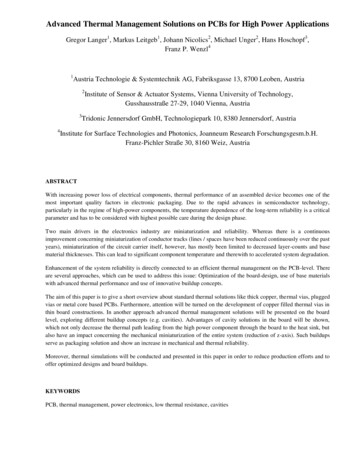
Chapter 1Introduction to Power MOSFETsA power metal-oxide-semiconductor field-effect-transistor (MOSFET) is a type of electricswitch that can be programmed through a digital signal processor to turn on and off.Power MOSFETs also have different voltage and current ratings, which can be used formany applications. Power MOSFETs are used in a wide variety of applications fromhome Do It Yourself projects to commercial projects. Some of the major uses for powerMOSFETs are inverters, buck and boost converts as well as AC/AC and DC/DCconverters. Figure 1.1 shows a single phase inverter using MOSFETs. Here Vd is thedrain to source voltage and Vo is the output voltage.Figure 1.1 Single Phase Inverter using MOSFETs1
The different topologies mentioned above can be applied to and are not limited to hybridand fully electric vehicles, solar panel systems, induction heating, electroshockweapons, and household appliances such as refrigerators or electric ovens. Todaythese devices are becoming more and more prominent in many different applications ascan be seen with vehicles transitioning more towards hybrid, electric, and autonomousvehicles. A major issue raised by power MOSFETs increase in use is their reliability andwhich trends and parameters should be taken into consideration in estimating remaininglifetime. These trends in the different parameters that can be measured may correlate tothe reliability of the device. For example, temperature monitoring of the device isimportant to make sure that it does not exceed the rating of the device specified by thedata sheet. In the industry, the reliability of these devices is very important because ofthe important applications they are used in. For instance, when purchasing a hybrid orelectric vehicle, the consumer will not want to go back to the dealership every thousandor five thousand miles driven to get the inverter replaced because the power MOSFETshave failed again. It is therefore vital to study MOSFET reliability, trends, andparameters so that they can be safely and efficiently used in important daily appliances.Not only can the failure or malfunction of power MOSFETs cause the inverter to getdamaged but it can cause other electric components such as the electric motor to failwithout the correct protection and will ultimately cause distrust between the consumerand the product. Monitoring key parameters such as threshold voltage, is a must tomake inverters and other topologies more reliable and efficient.2
Chapter 2Power MOSFET BackgroundThe following is a general description of the main properties and models of powerMOSFETs. The MOSFETs are examined are the V-MOSFET, VD-MOSFET, and the UMOSFET all from [8]. Different failure profiles of the devices are also explained.2.1 Power MOSFET2.1.1 V-MOSFET StructureThe V-MOSFET structure was developed in the 1970s. This structure has the 𝑁 source separated from the drain by a P-base region. As seen in figure 2.1.1 [8], the gateis a V-groove and goes through the P-base region into the N-drift region. The oxide ison the surface of the V-groove. Without any bias applied to the gate, 𝐽1 becomesreverse biased if the drain electrode has a positive bias applied to it. Next we have 𝐽2 ,which is overlapping the source electrode over the junction. It is noted that 𝐽2 is shortcircuited due to this overlap. When a positive gate bias is applied to the gate, it attractselectrons under the gate oxide to the semiconductor surface which provides a path forcurrent flow from the source and drain of the MOSFET. Here the internal resistance ofthe MOSFET restricts the maximum allowable current the MOSFET can carry. The VMOSFET structure is no longer used due to various manufacturing difficulties.3
Figure 2.1.1 V-MOSFET Structure2.1.2 VD-MOSFET StructureIn our experiment the VD-MOSFET is the MOSFET type that is used. The VDabbreviation stands for vertical-diffused. In this MOSFET the 𝑁 substrate is heavilydoped and the P-base is fairly weak. Figure 2.1.2 shows the VD MOSFET structure. Ifno bias is applied to the gate, a high positive DC link voltage can be applied across thedrain and source to form 𝐽1 . When this junction is formed between the P-base regionand the N-drift region, it becomes reverse biased. Here the N-drift region is lightlydoped. When a positive bias is applied to the gate, the current starts to flow across thedrain and source only after a positive drain voltage is applied. When these voltages areapplied an inversion layer can be formed, which will provide a path to transport4
electrons. This inversion layer is created in the P-base region. As the electrons movethrough the source region into the channel they then enter the N-drift region. Then theelectrons are transported through the JFET (Junction Field-Effect Transistor) region.When current flows in the JFET region, the internal resistance begins to increase. Sothe gate width has to be optimized in order to try and minimize the internal resistance ascurrent flows. The doping concentration of this region can also be doped more heavilyto try and reduce this resistance as the current flows through. As the current flowcontinues on its path, the electrons will again enter the N-drift region, only this timebelow 𝐽1 . The current in this region is nonuniform which creates a much largerresistance in the in the drift region. To reduce the effect of the JFET region, trench-gatepower MOSFETs started to be developed.Figure 2.1.2 VD-MOSFET Structure5
2.1.3 U-MOSFET StructureEtching trenches in silicon began in the 1980s. This technique was used to create theU-MOSFET which is also known as a trench-gate MOSFET. Figure 2.1.3 [8], shows thestructure of the U-MOSFET. It can be seen that the trench that surrounds the gate,spans from the source which is doped with 𝑁 , through the P-base region into the Ndrift region. The oxide is formed in the trench area, throughout the gate region. As withthe VD-MOSFET, if there is no bias applied to the gate, this structure can also support ahigh positive drain voltage. In figure 2.1.3 the junction, 𝐽1 , is formed between the N-driftregion and the P-base region which becomes reverse biased. Although the N-driftregion is fairly thick, is lightly doped. In order for drain current to begin to flow, a positivebias must be applied to the gate with a positive drain voltage. Once these conditions aremet the current will begin to flow. The current first flows through the P-base regionbecause of the inversion layer that is formed in the channel. Once the electrons movethrough the P-base region they will enter the N-drift region. In the U-MOSFET structurethere is no JFET region so that when the current spreads throughout the N-drift region,the internal resistance becomes greatly reduced compared to the VD-MOSFET. Thewidths of the N-drift regions will be taken equal to each other in order to show that whencomparing the VD-MOSFET to the U-MOSFET, the U-MOSFET has the lower internalresistance. This resistance was created to be smaller because in the VD-MOSFETsstructure, the internal resistance was greater than the turn-on resistance of the device.6
Figure 2.1.3 U-MOSFET Structure2.2 Failures Due to Thermomechanical StressesAs the temperature begins to rise in these devices, it starts to alter many physicalproperties which can change the physics of the devices themselves. The mechanicalparameters that can change the electrical parameters of the device are bond-wirecracking, bond-wire liftoff, die-attach degradation, and die-attach failure. Theseparameters can change the turn on resistance which can affect the electricalparameters of the device. Power cycling which leads to thermo-cycling is the maincause of these failures.7
2.2.1 Bond-wire Cracking and LiftoffBond-wire cracking and liftoff are the most prominent areas of failure for power devices[19]. Bond-wires degrade over time before these failures start occurring and over timewill cause a failure in the device. This is due to the applications they are used in and theenvironments they are placed working in. For example, in hybrid vehicles, when left outin the sun on a hot day, the whole inverter system gets even hotter than the ambientoutdoor temperature is because the heat is trapped. So if one was to turn the car onand have the cooling system kick on full power to cool off the devices, that temperaturefluctuation could start to cause this cracking or liftoff of the bond-wires. The main causeof the bond-wire liftoff is how the junction temperature fluctuates. If the junction its self isfluctuating from 20 C to 150 C or higher and it keeps repeating, then this type offailure is more likely. Also when systems are power cycled or thermo-cycled the junctiontemperature is most likely to fluctuate. In order to try and keep this failure fromhappening a cooling system must be integrated and used to control the junctiontemperature of the device. The device case temperature should also be monitored whencooling the device off. If cooling happens to fast causing the temperature of the deviceto go lower than it needs to go, the device then has to heat up causing the coolingsystem to shut off. This can lead to a temperature fluctuation process in which thedevice heats up too much and then gets cooled off too fast to a temperature lower thanneeded which would cause the bond-wires to crack or liftoff. Figure 2.2.1 from [20]shows the von-Mises distribution which leads to the bond-wire cracking.8
Figure 2.2.1 von-Mises DistributionA cooling system must have a control in which it moderately cools off a device and triesto keep the temperature within a small area of fluctuation in order to keep bond-wirecracking or liftoff to a minimum. Liftoff more prominently occurs when the temperature ofthe device is exceeded for long periods of time which can cause the solder on the bondwire to melt then causing the wire to liftoff. In a test done in [20] bond-wire liftoff due tobond-wire cracking can be seen in figure 2.2.2.Figure 2.2.2 Bond-wire Liftoff9
2.2.2 Die-attach Degradation and FailureDie-attach degradation and failure also occur due to thermomechanical stresses of thedevice. As the device is heated slowly and the temperature keeps rising, this form offailure is likely to happen [21]. This failure is not as likely to happen as bond-wire liftoff.Die-attach degradation causes the overheating of the gate oxide. The gate oxide cansubsequently burn and lead to an immediate failure in the device. As can be seen infigure 2.2.3 [22], as the die-attach solder begins to heat up it does not dissipate heat thesame way copper does. So as it heats up the properties of the materials will heat updifferently causing stress and the die-attach to start degrading and failing. The stressdirections on the materials can also be seen in figure 2.2.3. There are shear stresses onthe die-attach material and peeling stresses on the copper. This helps demonstrate howexactly the die-attach will begin to fail due to the stresses.Figure 2.2.3 Die-attach to Copper10
2.3 Electrical Failures of Power MOSFETsThe three types of electrical failures that will be briefly discussed are the gate oxidebreakdown, maximum drain to source voltage breakdown, and maximum drain currentbreakdown.2.3.1 Gate Oxide BreakdownGate oxide breakdown can be caused immediately or overtime. For the gate oxide tobreak down immediately, a very high voltage applied across the gate and source wouldbe needed. This voltage would have to exceed the maximum rating of the device by upto three or four times. The immediate breakdown due to overvoltage is unlikely tohappen in a real system due to protection circuitry from the gate drive. On the otherhand, over time the gate oxide will degrade due to potential over stresses on the device.This can happen in a normally operating device. Every time the MOSFET is switched onand off the voltage applied is an electrical stress to the gate. This means over time theoxide will degrade. When the oxide is degrading this means that the thickness of thedielectric material of the gate is decreasing throughout its life. As the oxide diminishes,this can cause an immediate failure of the oxide once it becomes too thin. After theoxide has degraded completely or it has broken after getting thin, the MOSFET willimmediately fail. Once the MOSFET fails due to the gate oxide degradation, the gate ofthe MOSFET will be shorted to the drain and source causing the gate drive to startsupplying more current and no voltage. At this point control of the gate is lost and theMOSFET is considered dead. Some MOSFETs have thicker gate oxide than others11
causing that gate to be stronger. This should allow the MOSFET to live longer sincethere is more gate oxide to degrade before it fails. Figure 2.3.1 [23] shows a highresolution transmission electron micrograph of a MOSFET before the oxide hasdegraded. Once this oxide has been fully degraded it will cause a short in the MOSFET.Figure 2.3.1 High Resolution Transmission ElectronMicrograph2.3.2 Maximum Drain to Source Voltage BreakdownAll power MOSFETs have a maximum drain to source voltage. This is considered thebreakdown voltage of the device. If this voltage is exceeded, then it will cause theMOSFET to enter the breakdown region. The drain to source terminal would then breakbecause the channel cannot sustain the voltage. All MOSFETS have differentbreakdown voltages. There are curves such as the one shown in figure 2.3.2 [24], that12
allow you to see the drain to source breakdown voltage with respect to the drain currentand the gate to source voltage. This figure displays a snapback breakdown effect.Figure 2.3.2 Snapback Breakdown13
Chapter 3Proposed Lifetime Theory3.1 IntroductionThis chapter will explain why and how gate oxide degradation plays a prominent role inpower MOSFET failure. A general theory has been proposed that power MOSFETs gothrough three operating regions as gate oxide degradation occurs. In region I, the gateoxide is not aged and considered to be fresh and healthy. In region II, the gate oxidehas started aging and the degradation of the oxide initiates. In region III, FowlerNordheim tunneling of electrons begins to occur in the gate oxide. The physics behindgate oxide degradation will be explained and shown with analytical equations that showa “dip and rebound” phenomenon in the threshold voltage throughout the threeoperating regions of the power MOSFET. The “dip and rebound” of threshold voltagewith the gate oxide degrading as it ages helps to determine the health of powerMOSFETs. This also provides an advanced warning for power MOSFET failures. Lastly,this pinpoints the instant of failure initiation due to oxide degradation and point of criticalfailure in power MOSFETs.Power MOSFETs are a crucial component of power converters used in high voltage andhigh power applications. Since the reliability of power MOSFETs is critical to theoperation of these power converters, effective forecasting of power MOSFET failures isessential. Prognosis can be defined as a forecast of a likely failure with the help of a14
failure precursor- an indicator of impending failure [1]. The key failure precursors ofpower MOSFETs with aging identified in the literature are: Threshold voltage, VTH [2][5], shift in threshold voltage [5], and switching time variations [6]. Aging and gate oxidedegradation are very closely related and plays a prominent role in power MOSFETfailure. However, the variation of the threshold voltage with aging due to oxidedegradation is not consistent across all literature. The threshold voltage (VTH) of apower MOSFET is reported to increase with aging [3]-[4], whereas other studies havefound the threshold voltage is to “dip and rebound” with aging [5]-[6]. To explain thisdifference in failure precursor variation with gate oxide degradation, the general theoryis proposed that power MOSFETs go through three distinct operating regions as gateoxide degradation occurs over time. The identification of three operating regionsalternatively helps us determine the “health” of power MOSFETs.1) Region I (Normal operation region):This region corresponds to the operation of power MOSFETs before the initiationof gate oxide degradation. The failure precursors remain constant in this region and donot affect the MOSFET which will be regarded as “healthy”.2) Region II (Operation after initiation of gate oxide degradation):The gate oxide, like any other dielectric, degrades over time. This regioncorresponds to the operation of power MOSFETs after the initiation of gate oxidedegradation. In this case, the MOSFET aging process has begun and started to take an15
effect and the failure precursors have begun to show some variation, “dip and rebound”with oxide degradation and the MOSFET can be regarded as “sick”.3) Region III (Operation after initiation of Fowler-Nordheim tunneling of electrons intothe oxide):With gradual gate oxide degradation, the oxide field increases to a point whereFowler-Nordheim tunneling [9] of electrons occurs in gate oxide and the failureprecursors start to show accelerated aging characteristics. The power MOSFEToperating in this region can be regarded as “dying”.3.2 General Theory for Identification of Key OperatingRegions in Power MOSFETsGate oxides, like any other dielectric, when stressed under an electric field degradesover time and eventually breaks down. The failure precursors of Power MOSFETs varywith gate oxide degradation. The identification of key operating regions of powerMOSFETs due to gate oxide degradation can be explained with the existing physics ofgate oxide degradation.I. Region I (Normal operation region)A fresh oxide has a finite dielectric thickness. The gate oxide is assumed tomaintain its thickness over a long period of time after which it slowly begins to degrade.The failure precursors remain constant in this operating region as the gate oxidedegradation and aging have not initiated yet.16
II. Region II (Operation after initiation of gate oxide degradation)Even with a very low field stress, the degradation of the gate oxide begins tooccur over time. The thermo-mechanical or (E) model explains the breakdown of SiO2oxide in terms of field enhanced bond breakage under low field stress [10]-[11]. The SiSi bond breakage leads to formation of traps which create localized conduction paths inthe oxide. The increase in localized conduction paths in the oxide can be consideredequivalent to thinning of the gate oxide, as indicated by t, a reduction of gate oxidethickness in figure 3.2a. We introduce the word “effective gate oxide thickness” to takeinto account the reduction of gate oxide thickness due to localized conduction paths asa result of charge trapping. The effective gate oxide thickness does not necessarilyindicate the uniform reduction of overall gate oxide thickness; rather it indicates thelocalized reduction of gate oxide thickness due to formation of localized conducting linksin the gate oxide.III. Region III (Operation after Initiation of Fowler-Nordheim tunneling of electrons intooxide)With continuous reduction of gate oxide thickness, the oxide field begins toincrease. When the oxide field is in the range of 5-7 MV/cm [12]-[14], Fow
home Do It Yourself projects to commercial projects. Some of the major uses for power MOSFETs are inverters, buck and boost converts as well as AC/AC and DC/DC converters. Figure 1.1 shows a single phase inverter using MOSFETs. Here Vd is the drain to source voltage and Vo is the outpu