Transcription
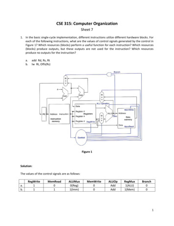
CSE 315: Computer OrganizationSheet 71. In the basic single-cycle implementation, different instructions utilize different hardware blocks. Foreach of the following instructions, what are the values of control signals generated by the control inFigure 1? Which resources (blocks) perform a useful function for each instruction? Which resources(blocks) produce outputs, but these outputs are not used for the instruction? Which resourcesproduce no outputs for the instruction?a.b.add Rd, Rs, Rtlw Rt, Offs(Rs)Figure 1Solution:The values of the control signals are as emWrite00ALUOpAddAddRegMux1(ALU)1(Mem)Branch001
ALUMux is the control signal that controls the Mux at the ALU input, 0 (Reg) selects the output of theregister file and 1 (Imm) selects the immediate from the instruction word as the second input to theALU.RegMux is the control signal that controls the Mux at the Data input to the register file, 0 (ALU) selectsthe output of the ALU and 1 (Mem) selects the output of memory.A value of X is a “don’t care” (does not matter if the signal is 0 or 1).Resources performing a useful function for the instruction are:a. All except Data Memory and branch Add unitb. All except Add unit and second read port of the RegistersThe Resources are as follows:a.b.Outputs that are not usedBranch AddBranch Add, second read port of RegistersNo outputsData MemoryNone (all units produce outputs)2. For the following logic blocks’ latencies, if the only thing we need to do in a processor is fetchconsecutive instructions (Figure 2), what would the cycle time be? Consider a datapath similar to theone in Figure 3, but for a processor that only has one type of instruction: unconditional PC-relativebranch. What would the cycle time be for this datapath? What if conditional PC-relative branch isthe only instruction n-extend20ps90psShift-left-22ps20psFigure 22
Figure 3Solution:I-Mem takes longer than the Add unit, so the clock cycle time is equal to the latency of the I-Mem:a. 400psb. 500psThe path for the unconditional PC-relative instruction is through the instruction memory, Sign-extendand Shift-left-2 to get the offset, Add unit to compute the new PC, and Mux to select that value insteadof PC 4. Thus, the cycle time will be as follows:a. 400ps 20ps 2ps 100ps 30ps 552psb. 500ps 90ps 20ps 150ps 100ps 860psConditional branches have the same long-latency path that computes the branch address asunconditional branches do. Additionally, they have a long-latency path that goes through Registers,Mux, and ALU to compute the PCSrc condition. The critical path is the longer of the two, and the paththrough PCSrc is longer for these latencies:a. 400ps 200ps 30ps 120ps 30ps 780psb. 500ps 220ps 100ps 180ps 100ps 1100ps3
3. Which kinds of instructions require each of the following resources? Assuming that we only supportbne and add instructions, discuss how changes in the latencies of this resource affect the cycle timeof the processor. Assume that the latencies of other resources do not change.a.b.Add 4 adder (The adder adding 4 to the PC)Data MemorySolution:The instructions that require the above resources:a. All instructions except jumps that are not PC-relative (jal, jalr, j, jr).b. Loads and stores.Of the two instructions (bne and add), bne has a longer critical path so it determines the clock cycletime. Note that every path for add is shorter or equal to the corresponding path for bne, so changes inunit latency will not affect this. As a result, we focus on how the unit’s latency affects the critical path ofbne:a. This unit is not on the critical path, so changes to its latency do not affect the clock cycle timeunless the latency of the unit becomes so large to create a new critical path through this unit,the branch add, and the PC Mux.b. This unit is not used by BNE nor by ADD, so it cannot affect the critical path for eitherinstruction.4. For the following single-cycle datapath MIPS instructions, using MIPS reference card, using registersnumbers as written explicitly in the instruction assembly form, what is the value of the instructionword? What is the register number supplied to the register file’s “Read register 1” input? Is thisregister actually read? How about “Read register 2”? How about “Write register”?Instructionlw 1, 40( 6)Label: bne 1, 2, Labela.b.Solution:The value of the instruction word:a.b.Binary100011 00110 00001 0000000000101000000101 00001 00010 1111111111111111Hexadecimal8CC100281422FFFFFor “read register 1” and “read register 2”, the registers numbers are as follows:a.Read register 16 (00110)Actually read?YesRead register 21 (00001)Actually read?Yes (but not used)4
b.1 (00001)Yes2 (00010)YesFor “write register”:Write register1 (00001)Either 2 (00010) or 31 (11111) (RegDst is X)a.b.Register actually written?YesNo5. What is the value of the following control signals for the jump instruction (Figure 4)?a. RegDstb. MemReadc. RegWrited. Jumpe. BranchFigure 4Solution:The values of the control signals are:a.RegDst X5
b.c.d.e.MemRead XRegWrite 0Jump 1Branch X6. The latencies of individual components of the datapath, shown in Figure 5, affect the clock cycletime of the entire datapath. Thus, for the following latencies, what is the clock cycle time if the onlytype of instructions we need to support are ALU instructions (add, and, etc )? What is the clockcycle time if we only had to support lw instructions? What is the clock cycle time if we must supportadd, beq, lw, and sw instructions? If we can improve the latency of one of the given datapathcomponents by 10%, which component should it be? What is the speed-up from this ign-extend20ps90psShift-left-20ps20psFigure 56
The longest-latency path for ALU operations is through I-Mem, Regs, Mux (to select ALU operand), ALU,and Mux (to select value for register write). Note that the only other path of interest is the PC-incrementpath through Add (PC 4) and Mux, which is much shorter. So for the I-Mem, Regs, Mux, ALU, Mux paththe latencies are:a. 400ps 200ps 30ps 120ps 30ps 780psb. 500ps 220ps 100ps 180ps 100ps 1100psThe longest-latency path for lw is through I-Mem, Regs, Mux (to select ALU input), ALU, D-Dem, andMux (to select what is written to register). The only other interesting paths are the PC-increment path(which is much shorter) and the path through Sign-extend unit in address computation instead ofthrough Registers. However, Regs has a longer latency than Sign-extend, so for I-Mem, Regs, Mux, ALU,D-Mem, and Mux path, the latencies are:a. 400ps 200ps 30ps 120ps 350ps 30ps 1130psb. 500ps 220ps 100ps 180ps 1000ps 100ps 2100psIn case of add, beq, lw, and sw instructions, the answer is the same as the above instructions, becausethe lw instruction has the longest critical path. The longest path for sw is shorter by one Mux latency (nowrite to register), and the longest path for add or bne is shorter by one D-Mem latency.The clock cycle time is determined by the critical path for the instruction that has the longest criticalpath. This is the lw instruction, and its critical path goes through I-Mem, Regs, Mux, ALU, D-Mem, andMux.a. I-Mem has the longest latency, so we reduce its latency from the 400ps to 360ps, making theclock cycle 40ps shorter. The speed-up achieved by reducing the clock cycle time is1130ps/1090ps 1.037b. D-Mem has the longest latency, so we reduce its latency from 1000ps to 900ps, making theclock cycle 100ps shorter. The speed-up achieved by reducing the clock cycle time is then2100ps/2000ps 1.0507. Consider the single-cycle datapath in Figure 5, for the instruction listed in table below, show thevalues of various control signals needed to execute instruction. Note that ALU function is ADD whenALUOp is 00, Subtract when ALUOp is 01 and determined by Funct part of instruction when ALUOpid 10 for R-type instructions.Solution:Memto Reg Mem MemInstruction RegDst ALUSrcBranchALUOpRegWrite Read WriteswX1X001000 (Add)beqX0X000101 (Subtract)7
8. We wish to add the instruction sll (shift left logical) to the single-cycle datapath shown in Figure 5.Add any necessary datapaths and control signals. Show any necessary addition for the table ofcontrol signals similar to that in Exercise 7, if needed.Solution:Instruction [10-6]ALUOp10Funct00 0000ALU Control1110 (shift left logical)Control actionShift the second ALU operand ( rt) by theamount in the shmat field (Instruction[10-6]), input to the ALU9. Repeat the above exercise for the instruction lui (load upper immediate).Solution:No modification to the datapath is required.We can add a new operation to the ALU.ALUOp11FunctXX XXXXALU Control1101 (shift left logical 16 bits)Control actionShift the second ALU operand(imm) 16 bits8
MemtoInstruction nchALUOp01110. Repeat the above exercise for the instruction jal (jump and link). You may find it easier to modify thedatapath in Figure 4 above.Solution:3122We already have a way to change the PC based on the specified address (using the datapath for the jinstruction), but we will need a way to put PC 4 into register ra (31), and this will require changing thedatapath.We can expand the multiplexor controlled by RegDst to include 31 as a new input. We can also expandthe multiplexor controlled by MemToReg to have PC 4 as an input. This requires changing the controllines of these two multiplexors from a single bit to two bits. The Jump control signal needs to be set to 1to operate as the j instruction. The register file will be enabled to 0RegWrite01MemRead00ALUOpXXXXBranchXXJump119
11. Assuming the latencies shown in the table below for single data path in Figure 5, what will be thelatency of each of the instructions: Add, Addi, lw, sw and beq.What is the maximum clock speed? Can we replace the adders by cheaper (slower) ones withoutaffecting the clock speed of the processor? In case your answer is no, explain why this is the case. Incase your answer is yes, compute the maximum latency for the adder that does not affect the ion:add latency 600 185 50 150 50 1035 psaddi latency 600 185 150 50 985 pslw latency 600 185 150 500 50 1485 pssw latency 600 185 150 500 1435 psbeq latency 600 185 150 935 psThe maximum clock speed is a 1/1485x10-12 673.4 MHzThere are two adders: one to compute the PC 4 and the other one to compute the branch address. Bothare not on the critical path of the instructions and can be replaced by slower adders. Note that the secondadder exists on 2 non-critical paths. If we call the adder latency X, we have the following constraintsPath1 latency: 2 X 50 1485 implying that X 717.5 psPath2 latency: 600 10 5 X 50 1485 implying that X 820 psTherefore the maximum adder latency of the adders that will not affect the processor speed is 717.5 ps.12. We wish to add a variant of the lw (load word) instruction to the single-cycle datapath shown inFigure 5. The instruction increments the index register after loading word from memory. Thisinstruction (l inc) corresponds to the following two instructions:lw rt, L( rs)addi rs, rs, 4Show the values of various control signal needed to implement the instruction. Is it possible tomodify the single-cycle implementation to implement this instruction without modifying the registerfile?. Explain why or why not.Solution:10
Write data 2The following modifications are required for the datapath: Perform autoincrement by adding 4 to register rs through an incrementer (add 4). Thisoperation is be done all the time. We need a second write port to the register file because two register writes are required forthis instruction. The RegWrite control signal will now be extended to two bits as shown inthe table below. A new “Write data 2” port will be added. We assume that the “Writeregister 2” identifier is always the same as “Read register 1” ( rs ). This way the setting“11” to control signal RegWrite indicates that there is second write to register file to theregister identified by "Read register 1" and the data is fed through “Write data 2”.Instruction RegDstl nchALUOp000This instruction requires two writes to the register file. The only way to implement it is to modifythe register file to have two write ports instead of one.11
Solution: I-Mem takes longer than the Add unit, so the clock cycle time is equal to the latency of the I-Mem: a. 400ps b. 500ps The path for the unconditional PC-relative instruction is through the instruction memory, Sign-extend and Shift-left-2 to get the offset, Add unit to compute