Transcription
This article has been accepted for inclusion in a future issue of this journal. Content is final as presented, with the exception of pagination.Photonic Integrated CircuitsUsing HeterogeneousIntegration on SiliconBy T IN KOMLJENOVIC , D UANNI H UANG , PAOLO P INTUS , Member IEEE, M INH A. T RAN ,M ICHAEL L. DAVENPORT, Student Member IEEE, AND J OHN E. B OWERS , Fellow IEEEABSTRACTHeterogeneous silicon photonics using wafer bonding is reaching maturity with commercial products forthe data center market being shipped in volume. Here wegive an overview of recent research in the area showingrecord device performance by using the best of both worlds:III–V for light generation and Si for guiding the light. Utilizingthe flexibility of the heterogeneous silicon platform, narrowlinewidth widely tunable lasers as well as fully integrated modelocked lasers with record pulse powers and pulse durationwere demonstrated. The ability to perform multiple die bonding with optimized epitaxially grown layer stacks was usedto realize high-performance photonic integrated circuits bothfor communications and sensing. In addition to III–V materials, nonreciprocal materials such as, for example, Ce:YIGcan be bonded, providing additional functionality such as onchip isolators and reconfigurable on-chip circulators. On-chipisolation will become necessary with the increase in complexityof photonic integrated chips as photonic components such aslasers are sensitive to feedback effects.KEYWORDS Heterogeneous silicon platform; integratedoptoelectronics; optoelectronic devices; semiconductor lasers;silicon photonicsI. I N T R O D U C T I O NPhotonics integrated circuits (PICs) can be realized ina number of platforms, but for efficient on-chip lightManuscript received October 12, 2017; revised June 27, 2018; acceptedAugust 6, 2018. This work was supported by the Defense Advanced ResearchProjects Agency (DARPA) under Direct On-Chip Digital Optical Synthesizer(DODOS), Photonically Optimized Embedded Microprocessors (POEM), and iWOGContracts. The views and conclusions contained in this document are those ofthe authors and should not be interpreted as representing official policies of theDefense Advanced Research Projects Agency (DARPA) or the U.S. Government.(Corresponding author: Tin Komljenovic.)T. Komljenovic, D. Huang, P. Pintus, M. A. Tran, and J. E. Bowers are withthe University of California at Santa Barbara, Santa Barbara, CA 93106 USA(e-mail: tkomljenovic@ece.ucsb.edu).M. L. Davenport was with the University of California at Santa Barbara,Santa Barbara, CA 93106 USA. He is now with Ayar Labs, Inc., Emeryville,CA 94608 USA.Digital Object Identifier 10.1109/JPROC.2018.2864668generation a direct bandgap semiconductor is needed.Historically, the first PICs with lasers were realized on GaAsor InP substrates [1]. The performance of lasers on nativeIII–V substrate is considered state of the art, but their highcost due to smaller wafer size and expensive substrates stillpresents a barrier to some markets.More recently, optical components have been integratedon silicon (Si) substrates. In the past 15 years, a wholerange of photonic components have been demonstrated,mostly using the silicon-on-insulator (SOI) platform. TheSOI platform is especially suited for standard communication bands at 1.31 and 1.55 µm, as both silicon and itsoxide SiO2 are transparent and form high-index contrast,high-confinement waveguides ideally suited for highlyintegrated PICs. However, electrically pumped efficientsources on silicon remain a challenge due to the indirectbandgap of silicon. There have been some demonstrationswith strained Ge, but the performance is very far frompractical products and the standards set by III–V on Si [2].Many current Si photonic PICs use hybrid approaches inwhich the Si PIC is coupled to III–V PIC which providesthe optical gain for lasers [3]. Such an approach requiresprecise alignment and arguably has scaling limitations.An alternative approach, most commonly called heterogeneous integration, bonds pieces of III–V material ontoa patterned Si wafer and then processes them togetherusing standard lithography tools. First demonstrated bythe University of California at Santa Barbara (UCSB) in2006 [4], such an approach is currently widely used byacademia (e.g., UCSB [5], [6], Ghent University [7], [8]),research organizations (e.g., III–V lab [9]), and industry(e.g., Intel [10], Juniper Networks (former Aurrion) [11],HP Enterprise [12]) with first commercial products fordata center market being shipped in volume [10]. Theadvantage of this approach is that the alignment tolerancesare significantly reduced as devices are defined lithographically after bonding of unpatterned III–V dies. This processallows for efficient volume scaling. Furthermore, the useof complementary metal–oxide–semiconductor (CMOS)0018-9219 2018 IEEE. Personal use is permitted, but republication/redistribution requires IEEE permission.See http://www.ieee.org/publications standards/publications/rights/index.html for more information.P ROCEEDINGS OF THE IEEE1
This article has been accepted for inclusion in a future issue of this journal. Content is final as presented, with the exception of pagination.Komljenovic et al.: Photonic Integrated Circuits Using Heterogeneous Integration on SiliconFig. 1.Evolution of photonic integration in terms of the number ofdevices in a single PIC. Silicon photonic integration (red circle)represents the “passive” integration without an on-chip lasersolution; InP integration (blue squares) and heterogeneous siliconintegration (green triangle) are solutions with on-chip lasers.processing infrastructure, perfected throughout the yearsand billions of dollars invested by semiconductor industry,allows for superior silicon waveguide quality with smallerfeature sizes, smoother surfaces, and superior yield. Thiswill become increasingly important as the complexity ofPICs increases, as shown in Fig. 1.The paper is organized as follows. In Section II, weintroduce the heterogeneous silicon platform, and provide brief literature overview and examples of individualdevices such as widely tunable lasers, mode-locked lasers,modulators, amplifiers, and photodetectors. The ability tobond multiple, smaller pieces of III–V allows for addedflexibility by combining multiple optimized epitaxial layerstacks to realize complex systems on chip. We describe thecapabilities of this approach in Section III, and provideexamples such as microwave generators, interferometricgyroscope front-ends, beam scanners, and a network-onchip with 2.56-Tb/s capacity. Bonding can be extended toother materials, which can be used to provide additionalfunctionality such as isolators (Ce:YIG) and second harmonic generation (LiNbO3 ). In Section IV, we report onon-chip isolators and circulators, both of which are reconfigurable. Finally, we summarize and give future outlook inSection V.technology of the SOI platform. Physically, the large mismatch in lattice constant and thermal expansion coefficientbetween the Si and III–V make monolithic integration verychallenging, although a lot of progress has been reportedas shown in [13]. Bonding removes, or at least relaxes,the lattice mismatch limitations to a very large degreealthough the thermal expansion coefficient mismatch stillhas to be taken care of. For this reason, the temperature during bonding and subsequent processing steps istypically limited to 300 C. There are two main bonding approaches that have developed: covalent moleculardirect bonding and adhesive bonding using polymers [14].The former is pursued by UCSB, Intel, Juniper, HPE, andIII–V labs among others, while the latter is pursued byGhent University among others.In a typical heterogeneous silicon process, waveguidesand other devices are first defined in a SOI wafer usingstandard CMOS-compatible processes. Next, pieces of III–Vmaterial are bonded and processed as shown in Fig. 2.As the pieces are typically larger than a single device,the alignment tolerances are significantly relaxed. Forhigh volume production, it is possible to simultaneouslybond across a full Si wafer with the help of a carrierwafer for the III–V pieces. The processing then continuesusing alignment marks defined on the SOI wafer, andbenefits from immersion DUV lithography commonly usedin CMOS.The SOI wafers are typically optimized for heterogeneous platform, and commonly have thicker Si devicelayer (400–500 nm) compared to the more commonlyused 220-nm-thick silicon photonics platform. The reasonis to facilitate more efficient coupling between active andpassive regions [8]. Another change in heterogeneoussilicon photonics is the reduction in buried oxide (BOX)thickness from the commonly used 2 to 1 µm, whichimproves thermal performance if laser is not flip-chipbonded. We have demonstrated up to 105 C lasing, andII. H E T E R O G E N E O U S S I L I C O NPHOTONIC DEVICESHeterogeneous silicon photonics1 works to provide thebest of both worlds: high-performance devices from optimized III–V materials and superior passive and waveguide1 When the heterogeneous approach was first demonstrated, thenomenclature “hybrid III–V silicon evanescent laser” was used and oftenshortened to “hybrid silicon laser.” In subsequent years, “heterogeneous”is more commonly used to describe this wafer scale approach to integration, and “hybrid” is more commonly used for bonding or solderingindividual dies onto a common substrate.2P ROCEEDINGS OF THE IEEEFig. 2.Simplified illustration of basic steps in a heterogeneoussilicon photonics fabrication process. A typical full run has15–20 lithography steps.
This article has been accepted for inclusion in a future issue of this journal. Content is final as presented, with the exception of pagination.Komljenovic et al.: Photonic Integrated Circuits Using Heterogeneous Integration on SiliconFig. 3.The fundamental TE mode in exemplary heterogeneousregion as width of underlying shallow etched Si waveguide ischanged. Corresponding Si waveguide widths are as follows:(a) 0.6 μm; (b) 0.8 μm; and (c) 1 μm. The color bar on the leftcorresponds to the index of refraction.commercial companies have shown up to 150 C lasing,which shows that higher thermal impedance of BOX layeris not the limiting factor in potential laser integration withelectronics.A common question relates to the yield of heterogeneousdevices. Generally, yield in both silicon and III–V processing is improved by the use of advanced lithography andprocessing tools. Wafer bonding yield is critically limitedby vertically protruding defects on the III–V chip (whichcan be avoided with prior inspection), and by particulatecontamination on both parts (Si and III–V), both of whichcan be further improved by transferring the process tomore advanced growth reactors and cleanrooms. The silicon wafer is virtually free of surface defects.For the covalent molecular direct bonding, a plasmaactivator is used to activate both the Si and InP wafersurfaces prior to bonding. The pieces are then placed incontact, which forms a spontaneous bond between thesurfaces. This bond is strengthened by placing the waferin a graphite clamp and annealing (typically at 300 Cfor 1 h). Trapped water vapor at the bonded interfacecan form voids during the bonding anneal, so the surfaceof the silicon is commonly patterned with an outgassingstructure [14].The optical mode in the heterogeneous region extends inboth the Si and III–V region, and the confinement can becontrolled with the width of Si waveguide, i.e., lithography,which is a powerful tool to engineer the modal profile asshown in Fig. 3. The transition between heterogeneousregion and passive Si waveguides is essential for highperforming devices: it should have low loss, low unintentional reflection, low transmission into higher orderwaveguide transverse modes (if supported), and highoptical bandwidth (for certain class of devices). Designmethodology and experimental characterization of a number of taper structures is presented in [15]–[18]. The transition may be accomplished in a number of ways, includinga lateral directional coupler, vertical directional coupler,a grating-assisted codirectional coupler, or an adiabaticcoupler. In our devices, we typically implement adiabatictapers (shown in Fig. 4) as they do not have intrinsicparasitic reflections and can be designed to have extremelylarge wavelength bandwidth [16].In the last ten years, many high-performing componentsrealized in the heterogeneous silicon platform have beendemonstrated, some of which outperform their nativeIII–V counterparts. In the remainder of Section II, wepresent a brief overview of devices developed for standardtelecommunication bands of 1.31 and 1.55µm. The heterogeneous platform has been extended, in recent years,beyond near-infrared telecommunication wavelengths tothe mid-infrared (MIR) (2–20 µm) regime using a numberof waveguide platforms (Si, SiO2 , SiN, Ge, etc.) and lasertechnologies such as InP Type-I and Type-II diodes; GaSbType-I diodes and intreband cascade laser (ICL) structures;and InP, GaAs, and InAs quantum cascade laser (QCL)structures. These wavelengths hold potential for an extensive range of sensing applications. The topic lies outsidethe scope of this paper, but a good overview is presentedin [19]. The heterogeneous approach can also be extendedtoward other waveguide systems, such as integration ofactive material on SiN waveguides that are transparentdown to 0.4 µm as demonstrated in [20]. It should bepointed out that due to the sheer number of publicationsin the area, the overview is to be illustrative and notexhaustive.A. Single-Frequency LasersSince the first demonstration in 2008 [21], heterogeneous silicon single-frequency distributed feedback (DFB)lasers have been continuously improved [22]–[24] andnow offer sub-10-mA thresholds, 5 mW of output power,high temperature lasing up to 100 C and high sidemode suppression ratio (SMSR) 55 dB. As the platformallows for the control of confinement in the quantum wells(QWs) and provides a low-loss waveguides, it opens up anew possibility in improving the coherence by providinga mechanism to separate the photon resonator (in Si)and highly absorbing active medium [25]. Initial demonstrations of heterogeneous DFB lasers with cavity qualityfactors in 106 range showed Lorentzian linewidths as lowas 18 kHz significantly outperforming native III–V DFBlasers. With further optimization, sub-kilohertz instantaneous linewidths were demonstrated [26]. Use of state-ofthe-art DUV lithography also allows for direct definition ofFig. 4.A 3-D mockup of the transition between heterogeneousand passive Si regions with dual layer tapers.P ROCEEDINGS OF THE IEEE3
This article has been accepted for inclusion in a future issue of this journal. Content is final as presented, with the exception of pagination.Komljenovic et al.: Photonic Integrated Circuits Using Heterogeneous Integration on SiliconFig. 5.Linewidth of widely tunable integrated lasers versus time.We make a distinction between III–V-based monolithic lasers, hybridlasers where individual III–V dies are bonded or soldered to acommon substrate, and heterogeneous integrated lasers wherelarger pieces of the III–V gain material are bonded to silicon.(Sampled grating distributed bragg reflector (SG–DBR), distributedproduction, and results with lower cost and potential forintegration into larger integrated circuits, such as photonically enhanced analog-to-digital converters (ADCs).There have been a number of demonstrations ofheterogeneously integrated mode-locked lasers withimproving performance [35]–[37]. Recently, 900-fs pulseswere demonstrated, which is the shortest for a modelocked laser on a silicon substrate with 98 mW of peakpower [17]. The passively-mode-locked RF linewidth was1.1 kHz, lowest ever demonstrated at 20 GHz. Twoother sub-picosecond fully integrated mode-locked lasers[38], [39], both realized in the monolithic InP platform,utilized racetrack-style lasers which typically have pooroutput power due to the inability to control the lasingdirection. The output power was not reported in eitherpublication.feedback (DFB), silicon-nitride (SiN), silicon-on-insulator (SOI).D. Semiconductor Optical Amplifiersthe grating, allowing such lasers to be mass produced on a300 mm wafer scale.B. Widely Tunable LasersChip-scale widely tunable lasers are important for bothcommunication and sensing applications, and they havea number of advantages such as size, weight, and costcompared to mechanically tuned counterparts. Furthermore, they allow for integration in more complex integrated photonic chips to realize added functionality. Widetunability in chip-scale semiconductor lasers is commonlyachieved by utilizing the Vernier effect. The effect hasbeen utilized both with sampled Bragg grating (SG–DBR)reflectors and ring resonators, but the use of ring resonators tends to be more common in heterogeneous silicondevices [27]. Ring resonators, provided that the utilizedwaveguide platform offers sufficiently low propagationlosses, have an advantage as the effective cavity length atring resonance is significantly enhanced, directly reducinglinewidth [28], [29].Heterogeneously integrated tunable lasers have beendemonstrated at both telecommunication bands (1.31 and1.55 µm) with wide-tuning range (54 nm), high SMSR( 45 nm), up to 18 mW of on-chip power and integratedlinewidths down to 50 kHz [9], [18], [30]–[34]. Linewidthis again superior compared to native III–V devices, asshown in Fig. 5 [27].C. Mode-Locked LasersThe mode-locked lasers are a special class of lasers thatproduce a time series of short optical pulses at radio frequencies. Integrated mode-locked laser diodes, similarly toon-chip widely tunable lasers, have an advantage in theirsmall size and capability for electrical pumping comparedto bulk crystal and fiber lasers. Utilizing advantages ofsemiconductor manufacturing technology allows for mass4P ROCEEDINGS OF THE IEEEAs the complexity of PICs increases (see Fig. 1), thesemiconductor optical amplifier (SOA) has become a critical component for many kinds of PICs to increase theoutput power and maintain signal levels as the signal propagates throughout a large number of optical components.Since the first SOA on Si demonstration in 2007 providing 13 dB of on-chip gain and 11 dBm of output saturationpower [40], the performance of heterogeneous SOAs wasagain continuously increased with subsequent demonstrations [16], [41]–[43]. Devices with up to 28 dB of on-chipgain [43] and output saturation powers of 16.8 dBmwere recently demonstrated [16]. As the heterogeneousplatform allows for continuous change of the confinementin the active region by changing the width of underlyingSi waveguide (Fig. 3), it is possible to design a SOA withboth high gain and the high output power.E. ModulatorsSilicon photonics inherently provides many phase tuning mechanisms. The most common method of achieving phase and amplitude modulation in silicon devicesis to exploit the plasma dispersion effect, in which theconcentration of free charges in silicon changes the realand imaginary parts of the refractive index. This can beaccomplished by using p-n and p-i-n junctions, or metal–oxide–semiconductor (MOS) junctions [44], [45]. Anothermethod is thermal tuning, which is reasonably efficient dueto large thermo–optic coefficient of silicon, but is too slowfor data transfer applications and has generally large staticpower consumption. All these methods primarily changethe phase, so a Mach–Zehnder interferometer or resonatorstructure (e.g., ring resonator) is employed to convertthe phase modulation to amplitude modulation. With theintroduction of germanium (Ge), small, efficient electroabsorption modulators utilizing the Franz–Keldysh effect arepossible with low leakage currents (47 nA @ -2 V) andbandwidths exceeding 50 GHz [46], but in this demonstration, the operating wavelength was limited to 1610 nm
This article has been accepted for inclusion in a future issue of this journal. Content is final as presented, with the exception of pagination.Komljenovic et al.: Photonic Integrated Circuits Using Heterogeneous Integration on Siliconor longer due to the increase in insertion loss at shorterwavelengths. Optimization of the operating wavelength ispossible by using SiGe, which shows 4.8-dB insertion lossat 1540 nm and up to 38-GHz bandwidth [47], but withlarger leakage current in the microampere range.The heterogeneous silicon platform allows for the use ofIII–V-material-based modulators. The use of III–V materialsbrings a number of advantages, such as large electroninduced refractive-index change, high electron mobility,and low carrier-plasma absorption, all of which are beneficial for overcoming the tradeoffs commonly encounteredwith modulators [48]. Furthermore, the state-of-the-artin QW design in III–V is currently superior to Ge/SiGe[49], [50] allowing for the utilization of quantum-confinedStark effect (QCSE) at arbitrary telecommunication wavelengths with devices fully integrated with standard SOIplatforms. Bandwidths in excess of 67 GHz, and data transmissions at 56 Gb/s were demonstrated [51]–[53]. TheQCSE is overall likely the strongest modulation mechanism[54]–[56], but very efficient modulators were also demonstrated in bulk III–V materials, especially if the SiSCAP typeof structure is used. Performance of III–V/Si modulatorssurpassed the performance of Si MOS optical modulators in terms of phase modulation efficiency by a factorof 5 (Vπ ·L 0.047 V·cm), while at the same time providinglower insertion loss [48], [57].F. PhotodetectorsSilicon, being transparent at standard communicationwavelengths of 1.31 and 1.55 µm, cannot be used fordetection at the same wavelengths. Detection, in silicon photonics, is commonly realized with the use ofGe. Ge-based waveguide detectors offer high bandwidths(45 or 67 GHz), good responsivities (0.8 or 0.74 A/W),and low dark currents in the nanoampere range [58],[59]. A problem is that the responsivities decrease as thewavelength of operation is increased beyond 1550 nm,leading to a direct tradeoff if Ge-based electroabsorptionmodulators are used as they tend to work better with lowerinsertion loss at longer wavelengths.In the heterogeneous platform, detectors can be basedon III–V material, often InGaAs that typically absorbs upto 1.7 µm with no drop in responsivity. The added flexibility of tailoring the Si waveguide width and the III–Vmesa width allows for flattening the absorption profileand suppressing the localized saturation leading to recordradio-frequency (RF) output power of 12 dBm at 40 GHz,which is the highest reported output power of high-speedwaveguide photodiodes for any waveguide photodiodetechnology, including native InP and Ge/Si [60]. Performance has been further optimized leading to high bandwidths (65 GHz) and record high RF output powers at 70GHz of –2 dBm with very low dark currents of 1 nA [61].Bandwidths exceeding 67 GHz (limited by measurementequipment) have also been demonstrated with a highresponsivity of 0.7 A/W [62].Fig. 6.(Left) A schematic of a 4-in SOI wafer with multiple III–Vepitaxial layers bonded on a single die. (Right) Photograph of a 4-inSOI wafer processed and bonded with III–V in the University ofCalifornia Santa Barbara cleanroom.III. S Y S T E M S O N C H I PA complex PIC might require a number of different, highperforming components. The underlying Si waveguidescan provide routing, multiplexing/demultiplexing, filtering, splitting, and combining. With some extra processing(implants and Ge), silicon photonics can also providemodulation and detection, albeit with some limitations, aspointed out in the previous section. The ability to bonddifferent epitaxially grown III–V thin films on a single dieallows for optimization of individual device performance.A complex PIC device might make use of optimized lasergain material, bandgap shifted modulator material as wellas optimized photodetector material, all on the same SOIdie as shown in Fig. 6. The corresponding monolithic III–VPIC would require multiple regrowth steps. With properdesign of the III–V layer stacks, simultaneous processingof all the different III–V layers after bonding is possible,reducing the number of processing steps, directly reducingcost and improving yield. The process also allows forfabrication of 1.31- and 1.55-µm devices on same waferas demonstrated in [11].This multiple-die bonding technology allows for stateof-the-art PICs for communications, signal generation, andsensing. We briefly describe a few key PIC demonstrationsin the remainder of this section. Furthermore, the scalability of CMOS processing and high volume production canbring the cost down, allowing PICs to enter markets wherepure III–V devices cannot compete due to price barriers.A. Microwave GeneratorThe broadband nature and low-loss capability of photonics has led to an ever-increasing interest in its usefor the generation, processing, control, and distributionof microwave and millimeter-wave (mm-wave) signals forapplications such as broadband wireless access networks,sensor networks, radar, satellite communitarians, instrumentation, and warfare systems [63]. One way to generatea microwave or mm-wave signal in the optical domainis based on optical heterodyning, in which two opticalwaves of different wavelengths are beat together on aP ROCEEDINGS OF THE IEEE5
This article has been accepted for inclusion in a future issue of this journal. Content is final as presented, with the exception of pagination.Komljenovic et al.: Photonic Integrated Circuits Using Heterogeneous Integration on SiliconFig. 7.(a) Optical microscope image of the fully integratedphotonic microwave generator chip and measured microwavesignals (b) from 1 to 50 GHz on an ESA, and (c) from 50 to 112 GHzon an E-band power meter.Such a device was recently demonstrated in theheterogeneous silicon platform [66]. This was a firstchip-scale fully integrated optical driver (IOD) that caninterrogate a sensing coil and realize an IFOG. The chipcomprises a light source (Fabry–Perot laser with broadoptical spectrum which is beneficial for gyroscope operation), three photodiodes (7-GHz bandwidth, 0.7-A/Wresponsivity, 4-nA dark current), two phase modulators (Vπ 4.2 V), and two broadband 3-dB splitters( 70-nm bandwidth) within an area of 4.5 mm2 , as shownin Fig. 8. A similar structure can be used in magnetometersand current sensors using special sensing waveguides orfibers [67], [68]. The size could also be further reducedwith different routing, resulting in a large reduction in size,weight, and power consumption, compared to current bulkvariants.C. Two-Dimensional Beam Scannerphotodetector. A chip-scale device providing that functionality has many advantages, most importantly size, weight,and cost. A fully integrated photonic microwave generatorrealized in the heterogeneous silicon platform combinedwaveguide photodiodes with a 3-dB bandwidth of 65 GHzand 0.4-A/W responsivity with lasers that tune over 42 nmand have 150-kHz linewidth. The microwave signal generated from beating two lasers together ranges from 1 to112 GHz. The inclusion of modulators allows for direct signal generation at the microwave frequency, or for generation of sidebands for, e.g., measurement applications [64].The total size of the chip was 14 mm 0.6 mm as shownin Fig. 7, but the length could significantly be reducedwith different routing, down to 3.5 mm. The laser wouldoccupy 2.5 mm of length, modulators 0.7 mm of length,and photodetectors with pads 0.3 mm of length. Thewidth of the chip would remain the same at 0.6 mm. Thiswould bring down the total area to 2.1 mm2 allowingfor fabrication of more than 25 000 devices from a single300-mm wafer.Free-space beamsteering is important for light detection and ranging (LIDAR), free-space communications,and has potential applications for holographic displaysand biomedical imaging. LIDAR employs a moving laserbeam to sample the environment for optical “echoes” andrapidly collect high-resolution 3-D images. In recent years,the research has intensified as a need for cost-efficient,lightweight LIDARs may be necessary for autonomousdriving.Photonic integration allows for integration of a phasedarray beamsteering system on a chip [69], with muchhigher stability and performance and lower cost thanhas been previously possible. The heterogeneous siliconPIC consists of 164 optical components including lasers,amplifiers, photodiodes, phase tuners, grating couplers,splitters, and a photonic crystal lens in 69 mm2 , as shownB. Interferometric Optical Gyroscope DriverInterferometric fiber optic gyroscopes (IFOGs) wereoriginally proposed in late 1960s and have been developed for decades. Today, IFOG is a mature technologywhich delivers high sensitivity, high stability, and reliability. A modern IFOG comprises five main components: apassive sensing fiber coil, a LiNbO3 chip with modulatorsand beam combiners, a laser, photodetectors, and readout electronics [65]. Most of the modern IFOGs still usediscrete optical components that are pigtailed and connected with the fiber coil to form a Sagnac reciprocalinterferometer. Use of bulk components results in largersize and high cost, especially if multiple rotation axesor redundancy is implemented. Integration could reducecost, weight, and size, and make the gyroscope morerobust to vibrations and shock, opening new applicationopportunities.6P ROCEEDINGS OF THE IEEEFig. 8.(a) Three-dimensional schematic of the integrated opticaldriver (IOD) for fiber optic gyroscopes. (b) Photo of a fabricated IODchip with closeups of its components. (c) A set of 12 IOD devicesnext to a U.S. quarter coin for size comparison.
This article has been accepted for inclusion in a future issue of this journal. Content is final as presented, with the exception of pagi
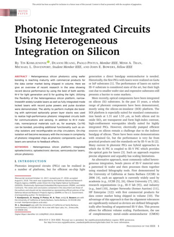
Photonic Integrated Circuits Using Heterogeneous Integration on Silicon By TIN KOMLJENOVIC,DUANNI HUANG,PAOLO PINTUS, Member IEEE,MINH A. TRAN, MICHAEL L. DAVENPORT, Student Member IEEE, AND JOHN E. BOWERS, Fellow IEEE ABSTRACT Heterogeneous silicon photonics u