Transcription
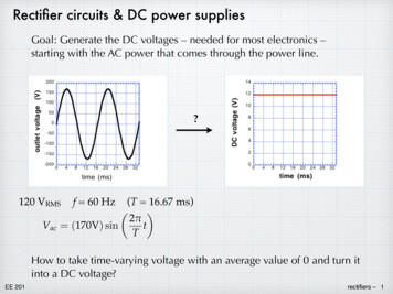
Rectifier circuits & DC power suppliesGoal: Generate the DC voltages – needed for most electronics –starting with the AC power that comes through the power line.?120 VRMSf 60 Hz ((T 16.67 ms)) sinHow to take time-varying voltage with an average value of 0 and turn itinto a DC voltage?EE 201rectifiers – 1
120 VRMStransformerpeak rectifierregulatorDC loadtransformer : reduces AC amplitude to something safe and manageable.Vpeak from the transformer will be a few volts bigger than the desired DCvoltage.peak rectifier : breaks up the AC waveform and produces a VDC Vpeak .regulator : Refines the output of the rectifier. (optional)Issues: Total power Efficiency Cost Load regulation (Does VDC change as the load draws differentamounts of current?) Line regulation (Does VDC change if the input AC amplitude changes?)EE 201rectifiers – 2
Half-wave rectifier() sinVS –Vp 3 V.Diode is off until VS 0.7 V.EE 201 vR–Resistor represent a load.We are trying to deliverDC power to the load.Current flows when diode is in forwardconduction. The output tracks the inputduring positive half cycle.rectifiers – 3
The diode turns off whenVS 0.7 V. It stays offduring the negative halfcycle of the sinusoid.VS 0:()VS 0:vR(t) 0:sin.(.) 0!To get the negative half of the cycle, turn the diode around.EE 201rectifiers – 4
Time delayNote that since the diode will not turn on until the sinusoid goes above 0.7 V, there is time delay before the rectifier “turns on”. It is a simplematter to determine the delay time, using the “on-off” diode model:3VSVo. 2sinarcsino0S .V , V (V)1diode off againoutputfollowsinput-1diode initially off-2If f 60 Hz (T 16.67 ms)and Vp 3 V, t’ 0.62 ms.-3timeThere is a similar time offset at the other end of the positive half cycle.The effect of the time offset become negligible if VP 0.7 V.EE 201rectifiers – 5
Peak rectifierAdd a largish capacitor after the diode, in parallel with the load.VSEE 201 –iDCiC iR vR–Initially, diode is on & cap chargesto VP - 0.7 V.VS –CiCiR vR–While VS vC , diode is off!Cap discharges through load.rectifiers – 6
VS –iDCiC iR vR–Diode stay off until VS comes backaround and becomes bigger thanvC. Then diode comes on againand re-charges the capacitor.EE 201When VS falls to less than vC, thediode turn off again, and the cyclecontinues.rectifiers – 7
Not a a perfect DC voltage atoutput. There is some variation(ripple) around an average value.00() .() [.] exp[.] exp t1T) [(t1 time when diode conducts again.EE 201t1 T().((])exp)rectifiers – 8
Example 1 () sinVS vo–C –T 16.67 msC 100 µFR 5000 !Find the average value of vo and the ripple voltage. Repeat for R 1000 ! and 200 !. [.] [.exp].exp()() 0.47 V(EE 201) () .R 1 k!R 200 !Vripple 2.19 VVripple 8.09 VVo (avg) 13.2 VVo (avg) 10.2 V. .Drawing more current causesthe ripple to increase and VDCto droop. Can fight this withmore capacitance.rectifiers – 9
Example 2 () sinVS vo–C –T 16.67 msR 1000 !Find the capacitance so that the ripple will be no bigger than 1 V.What is the DC voltage? [ (.]ln) exp .() .ln . 397 µF.What capacitance is needed to limit the ripple to 0.1 V?C 4000 µF !!!EE 201rectifiers – 10
Full-wave rectifierWith a few more diodes, we can rectify the entire sinusoidal input.1VS –43 vR–4orVS1– vR –232The diodes are in a bridge configuration.During the positive half cycle of the input, diodes 1 and 2 will beforward biased. Current will flow from the positive source through thosediodes and the resistor to generate a positive voltage across the resistor.During the negative half cycle of the input, diodes 3 and 4 will beforward biased. Current will flow from the negative source through thosediodes and the resistor to generate a positive voltage across the resistor,again.EE 201rectifiers – 11
1VS– vR –2iR4VS –– vR iR3Note that there are no two diode drops in the conduction path(s).Also, the frequency is effectively doubled.EE 201rectifiers – 12
Full-wave peak rectifierPlacing a capacitor in parallel with the load, turns the circuit into a fullwave peak rectifier. It behaves essentially the same as the half-wave peakrectifier except with twice the frequency (half the period).() sinVp 8 V.1VS –43CR vR–2The ripple voltage is calculated in exactly the same way, except that theperiod is cut in half (frequency doubled). [EE 201.]expSame as doublingcapacitance!rectifiers – 13
Example 3You want to use a wall transformer that produces 10-VRMS at the secondaryto generate a DC voltage. The desired voltage DC should be greater than12 V and it should be able to supply at least 50 mA while keeping thevoltage ripple to less than 5%. Design the rectifier to meet these goals.(Note: f 60 Hz.)10 VRMS 14.1 V amplitudeeffective RL Vo / Io 12.0 V / (50 mA) 240 !Note: This would be the minimum value of effective resistance. Ifwe choose C to meet the ripple requirement, then we will still besafe if we use a slightly higher Vo.Two options: half-wave or full-wave rectifier. Try both.Half-wave:Vo(max) Vp – 0.7 V 13.4 V Vripple 0.67 V. EE 201ln. 1350 µFVo(avg) Vo(max) – Vripple / 2 13.06 V.rectifiers – 14
Full-wave:Vo(max) Vp – 2(0.7 V) 12.74 V Vripple 0.64 V. ln() µVo(avg) Vo(max) – Vripple / 2 12.42 V.Either approach will work and meet the requirements. The full-waveversion uses extra diodes, but only half the capacitance. Since diodes arenearly free (pennies per piece), but big capacitors are relatively expensive,the full-wave circuit will actually cost less than the half-wave.This is why full-wave rectifiers are used more commonly than half-waverectifiers.Component manufactures supply full-wave bridge rectifiers packaged assingle unit with the transformer sinusoid as input the rectified waveform asthe output.EE 201rectifiers – 15
Nov 01, 2015 · nearly free (pennies per piece), but big capacitors are relatively expensive, the full-wave circuit will actually cost less than the half-wave. This is why full-wave rectifiers are used more commonly than half-wave rectifiers. Component m