Transcription
Operational Amplifiers: Basics and Design AspectsA tutorial by Jonathan Ames1
Table of Contents1.Operational Amplifier (Op-Amp) Basics. 41.1.Symbols and Schematic . 41.2.Kirchhoff’s Current Law applied to Op-amps . 61.3.Input/Output Impedance . 81.4.Supply voltages. 101.5.Open/Closed Loop Gain, Positive/Negative Feedback. 111.6.Frequency Response . 121.7.Basic Op-Amp Circuits. 131.7.1.Inverting amplifier . 131.7.2.Non-inverting amplifier . 141.7.3.Comparator . 151.7.4.Voltage follower . 162. Op-amp Circuits . 182.1.Derived Op-Amp Circuits. 182.1.1.Summation amplifier . 182.1.2.Integration . 192.1.3.Differentiation. 202.1.4.Differential amplifier . 212.2.Applied Op-Amp Circuits. 222.2.1.Audio amplifier. 222.2.2.Instrumentation amplifier. 242.2.3.Precision full-wave rectifier. 262.2.4.Voltage-to-Current converter. 273. Op-Amp Practical Considerations . 293.1.Input/Output Offset Voltage . 293.2.Input Bias Current / Input Offset Current . 293.3. Common Mode Rejection Ratio (CMRR) . 293.4.Output Short-Circuit Current . 304. Op-amp Circuit Design . 315. Conclusions. 396. References. 412
PrefaceThe objective of this tutorial is to provide students with a means of betterunderstanding the operational amplifier (op-amp). This comprehension is facilitated byfirst considering some of the fundamentals of op-amps, and from there using KCL circuitanalysis to explore and develop common op-amp circuits. Next, some practicalconsiderations are covered that view the op-amp from a real-world perspective whichvaries from the ideal. Finally, an op-amp circuit is actually constructed on a breadboardand oscilloscope prints are included to describe its operation and results. By readingthrough this tutorial a student should have a better understanding concerning operationalamplifiers and how they are analyzed.3
Chapter 11.Operational Amplifier (Op-Amp) Basics1.1.Symbols and SchematicBelow is the symbol used to represent an operational amplifier. The two inputsare the inverting (V-) and non-inverting (V ) terminals, and the output is Vout. Thesupplies are discussed further in the pages ahead.V supply-Inverting input(V-)Vout Non-inverting input(V )V-supplyFigure 1. Op-amp SymbolThe op-amp can be thought of as a “black box” having two inputs and one output as seenin Figure 2 below:Inverting inputNoninverting BlackBoxOutputFigure 2. Block diagram of an operational amplifier4
The op-amp can also be represented as a dependent voltage source (Vdep) as in Figure 3,having an output impedance (Zoutput) and input impedance (Zinput). The input impedance isso high that no current can flow between the input terminals, but the output impedance isvery low. The supply voltages provide the power necessary for the high gain andamplification and are viewed here as the dependent voltage source.ZoutputV-OutputZinput -VdepV Figure 3. Equivalent view of an op-ampThe circuitry that makes up an op-amp consists of transistors, resistors, diodes,and a couple capacitors. In general, these components are combined to achieve within theop-amp two stages of differential amplifiers and a common-collector amplifier. [1]In an effort to simplify the operational amplifier, one must not forget that theinternal circuitry of an op-amp is more than just a “black box”. All operational amplifiersare integrated circuits (ICs), and Figure 4 illustrates the components that work together toachieve what we know to be an op-amp.5
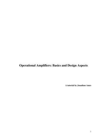
Figure 4. Internal circuitry of an op-amp [2]1.2.Kirchhoff’s Current Law applied to Op-ampsAn operational amplifier circuit can be analyzed with the use of a well-acceptedobservation known as Kirchhoff’s Current Law (KCL). KCL simply states that thecurrents entering a node are equal in magnitude to the currents leaving that same node. Anode is any junction wherein two or more two-terminal components meet. ConsiderFigure 5 for clarification.6
node60mA20mA40mAFigure 5. KCL definedIn this case, 20mA 40mA 60mA.The principle of KCL is the heart of node voltage analysis. The purpose of nodevoltage analysis is to find the voltage value at a certain node(s). This is done byrepresenting the currents entering and leaving the node by their Ohm’s law equivalent(i.e. I V/R). KCL and node voltage analysis apply to all electrical circuits includingoperational amplifiers. The following figure is a common non-inverting op-amp circuitthat will be repeated later on in the tutorial.RfIfRi(V-)(1)i-Iii (V )Vs Vout --Figure 6. KCL and op-ampsThe number (1) indicates the main node of significance. At this node, a current isassumed to leave the inverting terminal (V-) of the op-amp and go through Ri to ground.Another current is assumed to feed from the output back to the inverting input throughresistor Rf. The third current (i-) feeds into the inverting terminal, but i- always equals7
zero. In fact, there are two important assumptions that concern op-amps when it comes toKCL circuit analysis:Two very important assumptions:1) i i 0V V 2)In Figure 6, i- equals zero, so If equals Ii. The voltage drops are across theresistor, so the voltage value of the side to which the current is flowing is subtracted fromthe side that the current is coming from (or the side of higher potential). See the equationsbelow:I f IiVout V (V ) Gnd RfRiThe voltage source is connected directly to V , so V Vs V- , and Gnd always equalszero.Vout Vs Vs RfRiVout Vs VsVout Vs R f Vs VsRiÎRfRiRfVout 1 VsRiSimplifying further, we have determined the output voltage (Vout) to inputvoltage source (Vs) relationship. Op-amps can be accurately described by simplyrecognizing that i i- 0, and V V- , and then correctly applying KCL. Moreexamples of KCL circuit analysis are found in the pages ahead.1.3.Input/Output ImpedanceTwo positive aspects of operational amplifiers are that they have a very high inputimpedance and a very low output impedance. A high input impedance is a good thingbecause the surrounding circuit in which the op-amp is a part sees the op-amp as havinga large resistance, so nearly all of the voltage will be dropped across it, instead of, for8
example, it being dropped across the internal resistance of a preceding source. In relation,a low output impedance is like having a low internal resistance, so all of the outputvoltage leaving the op-amp will be dropped across the subsequent circuitry or load andnot very much of it will be lost across the internal resistance of the op-amp. A reasonableoutput impedance value could be between 0-100 Ω, while an input impedance could bearound 1 MΩ. [1,2]The figure below illustrates the benefits of a high input impedance and a low outputimpedance by introducing an op-amp circuit called a voltage follower which will berevisited again later in the tutorial.Rs 1kΩ -Rload 50ΩVs 5V(a)Zout 5Ω-Rs 1kΩ -Vs 5VZin 1MΩRload 50Ω(b)Figure 7. A simple voltage source and load with and without an op-amp voltage follower[1]ExampleFigure 7(a) shows a voltage source (5V) with an internal resistance (1kΩ) that ispowering a load (50Ω). Using the voltage divider formula, 50 5V 0.238V , 50 1k 9
only 0.238V actually gets dropped across the load while most of the voltage is droppedacross the internal resistance (Rs). This is a waste of useable load voltage.Now consider Figure 7(b) in which an op-amp is introduced with a high input impedance(Zin) and low output impedance (Zout). (Normally, input and output impedances are notrepresented this way.) The voltage source sees the high input impedance of the op-amp,so most of the voltage is dropped across this impedance rather than across the internalresistance of the source (Rs). 1MΩ 5V 4.995V 1MΩ 1kΩ Now the op-amp acts as the source, so 50 4.995V 4.541V 50 5 Because of the op-amp, the load now drops a voltage of 4.541V, instead of a mere0.238V. [1]1.4.Supply voltagesLooking at the op-amp symbol, the V supply and V-supply terminals are the dcsupply voltages. The output of the op-amp is influenced by these supply voltages in threeways. First of all, even if the supply voltages are 10V, the output will never span the20V range ( 10V Æ -10V). Rather, depending on the resistance of the load that the opamp is powering, the output will be 1V-2V shy of the supply voltage span. If theresistance of the load is greater than 10k then the output would max out between 9V and-9V, assuming the listed supply voltages are 10V. Otherwise, if the resistance of theload is between 2kΩ and 10kΩ then the output would max out between 8V and -8V,and even much less of a span for resistances of the load lower than 2kΩ. See thefollowing two examples:Example 1Supply voltages 10V; resistance of the load 20kΩSolutionResistance of load 10kΩ, so the output is 9VExample 2Supply voltages 12V and ground; resistance of the load 5kΩ10
Solution2kΩ Resistance of load 10kΩ, so the output is 2V to 10V.Second, the supply voltages are not always of the same value and of oppositepolarity (i.e. 5V). Instead, the max value could be 10V while the low value could be0V (or grounded) and vice versa, similar to Example 2 above.Finally, the output signal is clipped if it spans a larger voltage range than the supplyvoltages provide. For example, the output signal might have the potential to oscillatefrom -10V to 10V, but if the supply voltages are -5V and 5V, then the output will beclipped with a maximum value near 5V and a minimum value near -5V. [1-3]1.5.Open/Closed Loop Gain, teristicofoperational amplifiers is the very high gain achieved atthe output. In general, gain is calculated asVgain Vout/Vin,a ratio of the output voltage to the input voltage. An opamp amplifies the difference between one input and theother, while neither individual input is itself amplified.The output is positive if the non-inverting input is moreContradiction?KCLanalysisstronglymaintains that V V- for anyop-amp. Then, we are told thatthe difference between V andV- is what is amplified. Whichis it? Are they equal or are theyslightly different? In fact, bothstatements are true. Internal tothe op-amp circuitry, V doesequal V-, but externally the opamp functions as a black boxand amplifies the differencebetween the terminals.positive than the inverting input, and negative if the inverting input is more positive thanthe non-inverting input. The gain value of an op-amp can be as high as 200,000 whenthere is no physical connection between the output and either of the inputs. This is calledopen loop gain. However, if there is a connection between the output and the input,usually through a resistor, then a feedback network has been established, and the gain isnow a closed loop gain. [1-4]11
2V-3V Positive output,Open loop gain2V--3V Negative output,Open loop gain{b}{a} {c}Closed loop gainbecause of feedbackFigure 8. Gain and open/closed loops [2]The feedback is either negative or positive, but usually negative feedback is used.Positive feedback occurs when some of the output feeds the input in a way that boosts theinput value. Negative feedback exists when some of the output returns to the input, but itacts contrary to the input, in that it is of opposite polarity, and so diminishes the value ofthe input. When this input value is diminished then the difference between the inputs isalso diminished. So, the voltage gain of a closed loop op-amp due to negative feedback isless than that of the open-loop gain. However, it is very helpful that the gain can now becalculated according to the resistors involved, whereas open loop gain cannot be easilycalculated this way. Also, the bandwidth of the op-amp containing negative feedback isincreased for both inverting and non-inverting amplifiers. Both of these types ofamplifiers will be further discussed in the pages ahead. [1-4]1.6.Frequency ResponseThe frequency response of the op-amp is pretty straight forward. Basically, as theoperating frequency of the op-amp increases, the voltage gain decreases. Actually, it isonly after the cutoff frequency is reached that the attenuation of voltage gain startshappening. The cutoff frequency is defined as the frequency at which the open loop gainequals 70.7% of its maximum gain, or, equivalently, down 3 dB from the maximum gain.All frequencies lower than the cutoff frequency, even 0 Hz, see the max gain because theop-amp is a dc amplifier. Gain bandwidth product is a simple formula that relates closedloop gain (Acl), bandwidth (cutoff frequency, fco), and unity-gain frequency, as such:12
funity (Acl)(fco)Unity-gain frequency is the maximum frequency possible where the gain equals 1.Remember that a closed loop lowers the voltage gain, yet by lowering the voltage gain,higher operating frequencies are made available. So, depending on what is needed for thejob, a certain degree of flexibility is available. A high gain, low frequency (or bandwidth)arrangement is possible, as is a low gain, high bandwidth configuration, as long as theirproduct equals the unity-gain frequency. [1,2] See the figure below to better understandop-amp frequency response.70.7% of max gain( fco )maxgainGain(Gain 1)Frequency( funity )Figure 9. Gain and Frequency [1,2]1.7.Basic Op-Amp Circuits1.7.1.Inverting amplifierThe inverting amplifier makes use of negative feedback to the negative inputterminal. The negative terminal also receives the source signal which is inverted at theoutput. Consider the circuit in Figure 10 (arrows indicate assumed current flow):13
RfRiVs - Vout-Figure 10 Inverting amplifierUsing KCL, the characteristics of the inverting amplifier can be described.First, remember that V V- , and that i i- 0Vout V Vs V 0RfRiNote: V- equals zero because V- V 0Vout Vs 0RfRiVout 1.7.2.ÎRf VsR f VsRiRiVout Vs RfRiÎRfVout VsRiNon-inverting amplifierThe non-inverting amplifier is very similar to the inverting amplifier except thesignal is present at the non-inverting input and the output is of the same polarity as theinput (i.e. the signal is not inverted).14
RfRi VsVout --Figure 11 Non-inverting amplifierUsing KCL, the output can be related to the input and the resistors Rf and Ri.Again, V V- and i i- 0Vout V (V ) Gnd RfRiNote: V- V Vs, and Gnd always equals 0.Vout Vs Vs RfRiVout Vs R f Vs VsRi1.7.3.ÎÎVout Vs VsRfRiRfVout 1 VsRiComparatorA comparator is a device that can be used to compare an input voltage to areference voltage. The circuitry for comparators can vary in design and thereby vary inresults. This configuration uses a voltage divider to create the reference voltage. [2]15
V supplyR VsC1 -Vout-R1V-supplyFigure 12 Comparator [2]The inverting terminal of the op-amp is set at the reference voltage, which is:()R1V sup ply reference voltageR R1When the input signal (Vs) at the non-inverting input is greater than the reference voltageat the inverting input then Vout will equal the positive supply (V supply). Similarly, whenVs is less than the reference voltage, then Vout will equal the negative supply (V-supply).V-supply could be grounded, in which case Vout would be 0V whenever Vs is less than thereference voltage. Since there is no negative feedback in this circuit, KCL cannot be usedto describe the characteristics of the comparator. [2]1.7.4.Voltage followerAddressed earlier in the discussion on input and output impedance, the voltagefollower (or buffer) is an op-amp circuit that has its inverting input connected directly tothe output without a feedback resistor. Since the input always equals the output, the gainof a voltage follower equals one.V gain VoutVin(Vout Vin, so gain is 1)16
See Figure 13 and the following KCL analysis. VoutVs --Figure 13 Voltage followerAgain, V V-, and in this case V also equals the voltage source (Vs). Furthermore, theoutput (Vout) is equal to V-.V- Vout, and V Vs, therefore, Vs VoutVout 1VsThe benefit of using a voltage follower is the high input impedance and low outputimpedance of the op-amp that allows almost all of the voltage from a previous source tobe dropped across it. The op-amp can, in turn, feed the rest of the circuit with the higherdesired voltage. See the section on input/output impedance for clarification. [1]17
Chapter 22.Op-amp Circuits2.1.Derived Op-Amp Circuits2.1.1.Summation amplifierThe summation amplifier is an easily understood op-amp circuit that sums each ofthe inputs according the inverting amplifier output formula. In fact, the summationamplifier is very closely derived from the inverting amplifier. Only, instead of having asingle voltage source (Vs) and resistor (Ri), multiple sources converge on the invertinginput (V-), each having its own resistor (Ri). See the circuit below.Va RfRaRbVb(1) - Vout-Figure 14 Summation amplifier [2]KCL analysis for the summation amplifier goes like this at node (1):I Ra I Rb I Rf i 0Va V Vb V Vout V 0RaRbRfV 0 V- , soVa Vb Vout 0Ra Rb R f18
VV Output formula for summation amplifier Î Vout R f a b Ra Rb This formula can be seen as simply adding together the outputs of multiple invertingamplifiers. To illustrate this point, it can be rewritten as:Vout VaRf ( Vb )RfRaRbRegardless of how it is written, this formula is good for input voltage sources withdifferent values of Ra and Rb, as well as for cases where Ra Rb. However, if Ra Rb Rf, then the output formula clearly becomesVout (Va Vb )In this case, the summing amplifier is actually adding together the input voltage sources.Finally, note that the summation amplifier can sum as many input voltage sources asdesired. [1,2]2.1.2.IntegrationThe subject of calculus involves exercises in differentiation and integration ofwhich most students struggle in varying degrees to understand. Well, the amazingversatility and value of the op-amp can be seen in its ability to perform integration anddifferentiation. Integrators and differentiators, as they are called, are very similar andtheir circuits are simple to draw. The use of a capacitor is what makes the complexmathematical process possible. Consider the integrator circuit of Figure 15:CicRirVs Vout-Figure 15 Integrator circuit19
KCL analysis for the integrator can be accomplished by introducing the followingformula for the current through the capacitor: dV ic C c dt The current flowing through the capacitor fluctuates as time passes, so the above formulais necessary to describe it. The KCL analysis looks like this:i r ic 0Vs V dV C c 0RdtVc is the voltage across the capacitor, so Vc Vout – V- , andVs V d (Vout V ) C 0RdtV- 0, soVsdV C out 0dtRdVout1 VsdtRC2.1.3.tÎVout1 2 Vs dtRC t1DifferentiationDifferentiation is the counterpart to integration and by simply switching thelocation of the resistor (R) and capacitor (C), a differentiator circuit can be formed.Since a capacitor does not allow dc current to pass through it, the voltage sourcesassociated with the integrator and differentiator circuits are ac sources. See the circuitbelow.20
RirCic VsVout-Figure 16 Differentiator circuitThe KCL analysis for a differentiator is naturally similar to the analysis of the integrator. dV Once again, ic C c dt i r ic 0Vout V dV C c 0RdtV- 0 and Vc Vs – V-, soVoutdV C s 0Rdt2.1.4.ÎVout RCdVsdtDifferential amplifierRfRaRb Va -Vb -Rc Vout-Figure 17 Differential amplifier [6]21
The differential amplifier in the above figure can be analyzed according to KCLrules. Then, in order to demonstrate one of the more common concepts of a differentialamplifier, the resistors will be related to each other as follows:RfRa Rc xRb[6]The two nodal equations are,(1)Vb V V RbRcandVa V Vout V 0RaRf(2)Solve the first equation for V , and solve the second equation (2) for Vout ,V Vb RcRb RcandRf R Va fVout (V ) 1 Ra Ra Insert the V equivalent into the equation for Vout ,Vout Vb R cRb RcR R 1 f Va fRa Ra As previously mentioned, make Rc Rb(x) , and Rf/Ra x ,Vout Vb (Rb x )(1 x ) Va (x )Rb Rb xÎVout Vbx(1 x ) Va (x )(1 x )Vout x(Vb Va )With this differential amplifier, the difference between Vb and Va is amplified by a gainof x. [6]2.2.Applied Op-Amp Circuits2.2.1.Audio amplifierThe audio amplifier below is composed of a transistor sector and an op-ampsector. Consider first the transistor whose collector voltage feeds the inverting input ofthe op-amp.22
Figure 18 Audio amplifier [2]The base of transistor Q1 is biased with a voltage divider as follows:R2( VCC ) VbaseR1 R2The emitter voltage (Vemitter) is only a diode drop less than the base voltage Vbase .Vemitter Vbase 0.7The current through the emitter (Iemitter) is:I emitter Vemitter REThe voltage of the collector (Vcollector) is:Vcollector VCC V RCandandI emitter I collectorVRC (I collector )(RC )The collector voltage (Vcollector) feeds the inverting input of the op-amp, which is thesecond sector of the audio amplifier. KCL analysis of the op-amp proceeds as usual,assuming V V- Vcollector, and i i- 0.Vout V V Rf1Rf 2Solving for Vout and substituting Vcollector for V , we get: Rf1 1 Vout Vcollector R f2 [1,2]23
The advantage of using an audio amplifier that contains an op-amp is the expected highinput impedance and low output impedance. Also, both the transistor amplifier and theop-amp work together in the amplification process to achieve a high gain. [2]2.2.2.Instrumentation amplifierFigure 19 Instrumentation amplifier [2]Instrumentation amplifiers are a combination of three op-amps that are typicallygrouped into two stages. The first two op-amps comprise the first stage and each is a noninverting amplifier. The second stage is a differential amplifier that may or may not haveunity gain. An instrumentation amplifier is beneficial for several reasons:1. high input impedance, unlike the lower input impedance of a differential amplifierby itself2. high CMRR (see the pages ahead for a better understanding of CMRR); thesource internal resistances of v1 and v2 do not affect the total resistance on eachinput arm3. good for smaller, insignificant input signals4. gain of the non-inverting amplifiers (first stage) can be varied by the rheostat(RC). [1-3]24
Now consider the KCL analysis for the first stage of the instrumentation amplifier. It ishelpful to redraw op-amps A and B and their corresponding circuitry for analysis.v1 vAA-v1R1 RCRCv2R2 -v2(a)BvB (b)Figure 20 First stage of instrumentation amplifier redrawn for each op-ampThe KCL for op-amp A is as follows:v A v1 v 2 v1 0R1RCSolve for vA, R R v A v1 1 1 1 v 2RC RC The KCL for op-amp B is as follows:v B v 2 v1 v 2 0R2RCSolve for vB, R R v B v 2 1 2 v1 2 RC RC The values vA and vB are the two inputs into the differential amplifier. Refer back to theanalysis of the differential amplifier and see that the output is one input minus the other,and this difference is multiplied by x, which is the gain. In the case of the instrumentationamplifier, the output is (vA - vB) if the differential amplifier has unity gain, or x(vA – vB)if it has gain.Either way, vA – vB equals:25
R1 R1 v1 1 RC RC v 2 RR2 v1 2 v 2 1 RC RC which equals,RRRRR1 R 2 R1 R 2 v1 v1 1 1 v 2 v 2 2 v 2 2 v1 Î v1 1 v 2 1 ÎRCRCRC RC RC RC RC RC RR 1 1 2 (v1 v 2 ) RC RC 2R (v1 v 2 )If R1 R2, then v A v B 1 RC 2R .Notice that the first stage has a gain of 1 RC If the differential amplifier has a gain value (x), then the final output would be theproduct of the two gains multiplied by the difference between the two input voltages, or 2R (v1 v 2 )Final output (x ) 1 RC [1-3]2.2.3.Precision full-wave rectifierThe precision full-wave rectifier receives an ac signal and produces a fullyrectified output. The second op-amp (2) is a summation op-amp, and the first (1) is aninverting amplifier with two diodes (D1 and D2), which make the rectification possible.The first op-amp inverts the signal but does not amplify it.RaRaRaVinRa/212Vout1RaVout2Figure 21 Precision rectifier (full-wave) [1]26
The two conditions possible are a positive or negative alternation. On the positivealternation, the op-amp inverts the signal, producing a negative value that conductsthrough D2 and the feedback loop. The output (Vout1) is –Vin. On the negative alternation,the op-amp again inverts the signal, and this time produces a positive value that does notconduct through D2, so the output is zero. Instead, the positive signal feeds D1 to avoidsaturation. Using an op-amp along with diodes for rectification is an asset becausewithout the op-amp, the typical 0.7V drop across a diode has to be taken into account. So,a small signal like 0.5V would not be rectified because the diode needs at least 0.7V toconduct. [1,3]The KCL analysis for each op-amp in the precision full-wave rectifier is detailed below:Op-amp 1Positive alternationVin V Vout1 V 0 ÎRaRaNegative alternation: Vout1 0Vout1 -Vinnote: V- V 0Op-amp 2Positive alternation Vin V Vin V Vout 2 V 0 Î Vout2 VinRa 2RaRaNegative alternation0 V Vin V Vout 2 V 0 Î Vout2 -VinRa 2RaRanote: Vin is negative, so –(-Vin) VinIt is helpful to consider the waveforms given in the figure (TP1-3).[1,3]2.2.4.Voltage-to-Current converterThe concept of the voltage-to-current converter may seem quite radical at firstbecause, in general, everyone agrees that if a resistance increases then the currentnaturally decreases (I V/R).27
Figure 22 V-to-C converter [5]But with the voltage to current converter, an increase or decrease in the load resistancehas nothing to do with the amount of current flowing through it. The non-inverting input(V V1 in the figure) will change with the load resistance, but the current through theload will change only according to Vin and/or R. See the KCL analysis below:Vout V V RRÎ[3,5]Vout 2V- 2V 2V1Vin V Vout V V RRRloadSubstituting 2V for Vout we get,VinV I loadRRload[3,5]28
Chapter 33.Op-Amp Practical Considerations3.1.Input/Output Offset VoltageOp-amps do not always perform practically as they should theoretically. Forexample, sometimes an output voltage exists when both inputs are grounded. This outputvoltage is called output offset voltage and it is caused by an input offset voltage. If one isknown the other can be calculated,Vio VooAvImperfect transistors contained in the differential amplifier are responsible for the inputoffset voltage, which is usually no more than 2mV. The offset null pins on the IC op-ampcan be used with a potentiometer to take care of Vio and Voo. [1-3]3.2.Input Bias Current / Input Offset CurrentSimilar to the offset voltages, there are currents flowing in or out of the inputs,and their average is known as input bias current, which may have a value of 80nA . Thecurrents on each input are not always equal and the difference between them is the inputoffset current. This is important because if the input bias currents are different, then theoutput voltage can be affected. So to keep the currents the same, each input needs to seethe same resistance to ground, since identical currents will flow through identicalresi
7 Figure 5. KCL defined In this case, 20mA 40mA 60mA. The principle of KCL is the hear