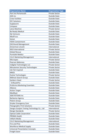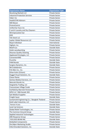
Transcription
Computer Organizationand Architecture/Introductionto Computer Organizationand ArchitectureDCAP502/DCAP206EditorDr. Manmohan Sharma
www.lpude.inDIRECTORATE OF DISTANCE EDUCATIONCOMPUTER ORGANIZATION ANDARCHITECTURE/INTRODUCTION TOCOMPUTER ORGANIZATION ANDARCHITECTUREEdited ByDr. Manmohan Sharma
ISBN: 978-93-87034-67-9Printed byEXCEL BOOKS PRIVATE LIMITEDRegd. Office: E-77, South Ext. Part-I, Delhi-110049Corporate Office: 1E/14, Jhandewalan Extension, New Delhi-110055 91-8800697053, celbooks.comforLovely Professional UniversityPhagwara
CONTENTSUnit 1:Review of Basics of Digital ElectronicsAnuj Sharma, Lovely Professional University1Unit 2:Devices Used in Digital ElectronicsSahil Rampal, Lovely Professional University23Unit 3:Data Representation and Data TransferYadwinder Singh, Lovely Professional University43Unit 4:Computer Organization IAvinash Bhagat, Lovely Professional University65Unit 5:Computer Organization IIAvinash Bhagat, Lovely Professional University81Unit 6:Control UnitPooja Gupta, Lovely Professional University95Unit 7:Central Processing UnitManmohan Sharma, Lovely Professional University111Unit 8:Addressing ModesAjay Kirani Khuswaha, Lovely Professional University125Unit 9:Computer Arithmetic ISarabjit Kumar, Lovely Professional University143Unit 10:Computer Arithmetic IIAvinash Bhagat, Lovely Professional University155Unit 11:Input/Output OrganizationAjay Kumar Bansal, Lovely Professional University165Unit 12:Memory Organization ConceptsPooja Gupta, Lovely Professional University185Unit 13:MultiprocessorsManmohan Sharma, Lovely Professional University205Unit 14:Introduction to Parallel ProcessingYadwinder Singh, Lovely Professional University229
SYLLABUSComputer Organization and Architecture/Introduction toComputer Organization and ArchitectureObjectives: The objectives of this course are: Tounderstand how computers are constructed out of a set of functional units Tounderstand how these functional units operate, interact and communicate Tounderstand the factors and trade-offs that affect computer performance Tounderstand concrete representation of data at the machine level Tounderstand how computations are actually performed at the machine level Tounderstand how problems expressed by humans are expressed as binary strings in a machineDCAP502 COMPUTER ORGANIZATION AND ARCHITECTURESr. No.Description1.Review of Basics of Digital Electronics: Codes, logic gates, flip flops, registers, counters, multiplexer,demultiplexer, decoder, and encoder.2.Integers Representation: Signed Magnitude, 1s & 2s Complement) & Real numbers (Fixed point &Floating Point representation), Register Transfer and Micro operations: Register transfer language Bus& memory transfer, logic micro operation, shift micro operation, Arithmetic Logic Shift Unit3.Basic Computer Organization: Instruction codes, computer instructions, timing & control, instructioncycles4.Memory reference instruction, Input/output & interrupts, Design of basic computer Control Unit:Hardwired vs. micro programmed control unit, Control Memory, Address Sequencing, Micro programSequencer5.Central Processing Unit: General register organization, stack organization, instruction format,Addressing Modes Data transfer & manipulation, program control, RISC, CISC.6.Introduction to Parallel Processing: Pipelining, Instruction pipeline, RISC Pipeline, Vector Processing7.Computer Arithmetic: Addition, Subtraction, Multiplication & Division Algorithm(s),Decimal arithmetic units & Operations.8.Input-Output Organization: Peripheral devices, I/O interface, data transfer schemes, program control,interrupt, DMA transfer, I/O Processor9.Memory Organization Concepts: Cache & Virtual memory10.Multiprocessors: Characteristics, Interconnection Structures, Interprocessor Communication andsynchronization
DCAP206 INTRODUCTION TO COMPUTER ORGANIZATION & ARCHITECTURESr. No.Description1.Tools for course understanding: Awareness of ISA bus interface, a popular bus architecture used inIBM and compatible personal computer systems.Digital Logic Circuits: Digital computers, Logic gates, Boolean Algebra, Map Simplification, HalfAdder, Full Adder, Flip flops – SR, JK, D, T, Edge triggered flip flops, Sequential Circuits2.Digital Components: Integrated circuits, Decoders – NAND gate decoder, Encoders, Multiplexers,Demultiplexers, Registers, Shift registers, Bidirectional Register with parallel load, Binary counters,Memory Unit – RAM, ROM, Types of ROMs3.Data Representation: Number systems – decimal, octal, hexadecimal, Complement – (r-1)’scomplement, r’s complement, Fixed point representation, floating point representation, Gray code,Decimal codes, alphanumeric codes, Error detection codes4.Register Transfer and Micro-operations: Register transfer language, Register transfer, Bus andmemory transfers – three state bus buffers, Arithmetic micro-operations – binary adder, binary addersubtractor, binary incrementer, arithmetic circuit5.Logic micro-operations and its hardware implementation, Shift micro-operations and hardwareimplementation, Arithmetic Logic Shift unit, Hardware description languages6.Basic Computer Organization and Design: Instruction Codes, Stored program organization,Computer registers, Common bus system, Computer instructions, Timing and Control, Instructioncycle, Memory reference instructions, Input output and interrupt, complete design of basic computer7.Central Processing Unit: General register organization, control word, Stack organization, registerstack, memory stack, Instruction formats – three address, two address, one address, zero addressinstructions, Addressing modes, Data transfer and manipulation, arithmetic, logical, bitmanipulation, Program control, Reduced Instruction Set Computer (RISC), CISC characteristics8.Input-Output Organization: Input output interface, I/O bus and interface modules, I/O vs memorybus, Isolated vs Memory mapped I/O9.Asynchronous data transfer, handshaking, Programmed I/O, Interrupt-initiated I/O, PriorityInterrupt – Daisy chaining, parallel priority, priority encoder, interrupt cycle, DMA controller andtransfer10.Memory Organization: Memory hierarchy, RAM, ROM chips, memory address map, Associativememory, Cache memory, Virtual memory, Memory management hardware
Anuj Sharma, Lovely Professional UniversityUnit 1: Review of Basics of Digital ElectronicsNotesUnit 1: Review of Basics of Digital ElectronicsCONTENTSObjectivesIntroduction1.1 Codes in Digital Electronics1.1.1 Classification of Binary Codes1.2 Logic Gates1.3 Summary1.4 Keywords1.5 Self Assessment1.6 Review Questions1.7 Further ReadingsObjectivesAfter studying this unit, you will be able to: Discuss the codes in digital electronicsList the functions of different logic gatesDiscuss the truth table for all the logic gatesIntroductionDigital electronics is a field of computer science. It deals with devices that are used to carry outcomputer applications.In digital electronics, we use two-state or binary logic. The two logic states are “0” (low) and “1”(high).Computer uses binary number system for its operations. Digital electronics represents the twobinary numbers, 1 and 0, using two voltage levels in a device called a logic gate. Sometimes thetwo states can also be represented using Boolean logic functions, “true” or “false” states, or usingan “on” or “off” state.Logic gates are important components of a digital circuit. A logic gate takes two inputs andgenerates a single output. In this unit we will discuss about the basic logic gates and theircorresponding truth tables.1.1 Codes in Digital ElectronicsBasically, digital data is represented, stored, and transmitted as groups of binary digits which arecalled bits. The group of bits is known as binary code. Binary codes are used in computers as theyallow computers to perform complex calculations quickly and efficiently. Binary codes are usedin financial, commercial, and industrial applications. To understand how binary codes are appliedin these fields, we first have to understand the classification of binary codes.1.1.1Classification of Binary CodesBinary codes can be represented as numbers and letters of the alphabets as well as many specialcharacters and control functions. They are classified as numeric or alphanumeric codes. Numericcodes are used to represent numbers, whereas alphanumeric codes are used to represent alphabeticletters and numerals.LOVELY PROFESSIONAL UNIVERSITY1
Computer Organization and Architecture/Introduction to Computer Organization and ArchitectureNotesThe binary codes are classified as shown in figure 1.1.Figur e 1.1: Classification of Binary CodesAs mentioned earlier, numeric codes are used to represent numbers. The following are the numericcodes:1.Weighted Binary Codes: Weighted binary codes are those which follow the positional weightingprinciples. In weighted codes, each position of the number represents a specific weight. Forexample, in decimal code, if the number is 345, then the weight of 3 is 100, 4 is 10, and 5 is 1. Inthe 8421 weighted binary code, each digit has a weight of 8, 4, 2 or 1 corresponding to itsposition.2.Non-Weighted Binary Codes: Non-weighted codes do not follow the positional weightingprinciples. In non-weighted codes, each digit position within the number does not have anyfixed value.Example: The codes 8421, 2421 and 5211 are examples of weighted binary codes.Example:Excess-3 and Gray codes are examples of non-weighted codes. Excess-3 codes areused to express decimal numbers. The code can be derived from the natural BCD (8421) code byadding 3 (011 in binary) to the coded number. It is used in decimal arithmetic units. The excess-3code of 1000 in 8421 is 1011. Gray codes represent each number in the sequence of integers {0.2 N1} as a binary string of length N such that the adjacent integers have Gray code representationswhich differ in only one bit position.3.2Reflective Codes: A code is said to be reflective when the code for 9 is complement for the codefor 0, 8 for 1, 7 for 2, 6 for 3, and 5 for 4.LOVELY PROFESSIONAL UNIVERSITY
Unit 1: Review of Basics of Digital ElectronicsNotesExample: Codes 2421 and excess-3 are reflective. In code 2421: we know that the positionalweights are 2, 4, 2 and 1. The following figure shows an example of reflective code where thecomplement of 8 is 1 and the complement of 7 is 2.4.Sequential Codes: Sequential codes are codes in which the succeeding code is one binarynumber greater than its preceding code. This assists in mathematical data manipulation.Example: 8421 and excess-3 codes are sequential codes.5.Cyclic Codes: In cyclic codes, only one bit in the code changes at a time while moving from onenumber to the next. It is a non-weighted code, which means that the position of bit does notcontain any weight.Table1.1 shows the bit patterns assigned for gray code from decimal 0 to 10.Table 1.1: Decimal Code to Gray Code Conver sion6.Decimal codeGray 1101101111Error Detecting Codes: Whenever data is transmitted from one point to another, there is aprobability that the data may get corrupted. In order to detect these data errors, some specialcodes called error detection codes are used.LOVELY PROFESSIONAL UNIVERSITY3
Computer Organization and Architecture/Introduction to Computer Organization and ArchitectureNotes7.Error Correcting Codes: These codes not only detect errors in data, but also correct themsignificantly. Error correction codes are a method by which a set of symbols can be representedsuch that even if any 1 bit of the representation gets accidentally flipped, we can still clearlyidentify the earlier symbol. Error correcting codes depend mainly on the notations and resultsof linear algebra. Error correction can be done using many methods like parity checking,Hamming codes, Single-bit Error Correction Double-bit Error Correction (SECDED), and soon.Notes Error correcting codes are used in memories, networking, CDROM, and so on.Example: Error correction using parity checking is as follows:In parity check, an extra bit is added to the binary number to make all the digitsin the binary number to sum up to an even or odd value. When the number addsup to an even number, we call it even parity and when the number sums up to anodd number, we call it odd parity. Consider the following two binary numbers:10110101101011Now, if we want to use even parity, we can add a parity bit to these numbers toobtain an even number as shown below:010110104111010116If we want to use odd parity, we can add a parity bit to the number as follows:110110105011010115Most of the modern applications use even parity. Let us consider even parity inour example.The two binary numbers that need to be transmitted are:01011010 .The even parity11101011 .The even paritySuppose during transmission the bits get changed as follows:011110105101010115We can observe that the digits in the number sum up to odd numbers. Since weare using even parity, the computer knows that there is an error in thetransmission.8.Alphanumeric Codes: These are codes that consist of both numbers and alphabets. The mostcommonly used alphanumeric codes are ASCII and EBCDIC.(a)4EBCDIC Code: EBCDIC (Extended Binary Coded Decimal Interchange) is mainly usedwith large computer systems like mainframe computers. It is an 8-bit code whichaccommodates up to 256 characters.LOVELY PROFESSIONAL UNIVERSITY
Unit 1: Review of Basics of Digital Electronics(b)ASCII Code: ASCII (American Standard Code for Information Interchange) has becomea standard alphanumeric code for microcomputers and computers. It is a 7-bit code,which represents 128 different characters. These 128 characters include 52 alphabets,which include A to Z and a to z, numbers from 0 to 9 (that is, 10 numbers), 33 specialcharacters and symbols, and 33 control characters.Notes1.2 Logic GatesA logic gate is an electronic device that makes logical decisions based on the different combinationsof digital signals available on its inputs. A digital logic gate can have more than one input signalbut has only one digital output signal.Integrated Circuits or ICs can be grouped together into families according to the number oftransistors or gates. Integrated circuits are categorized according to the number of logic gates orthe circuit complexities within a chip.AND GateAND gate is a type of digital logic gate, which has an output that is normally at logic level “0”and goes “HIGH” to a logic level “1” when all of its inputs are at logic level “1”. The output ofAND gate returns “LOW” when any of its inputs are at a logic level “0”.The Boolean expression for AND gate is Q A.B.A simple 2-input logic AND gate can be constructed using RTL structure connected together asshown below in figure 1.2. Both transistors, T 1 and T2 must be saturated “ON” to produce an outputat Q. In the figure 1.2, we can observe that the output from T 1 is the input to T2. Vcc is the input totransistor 1 and the final output, Q A.B, is obtained from T 2.Figure 1. 2: Design of AND GateLOVELY PROFESSIONAL UNIVERSITY5
Computer Organization and Architecture/Introduction to Computer Organization and ArchitectureNotesThe figure 1.3 shows the truth table and symbol of AND gate.Figure 1.3: Logic Sym bol an d Truth Table of ANDGateExample: Commonly available digital logic AND gate ICs are:TTL Logic Types74LS08 Quad 2-input74LS11 Triple 3-input74LS21 Dual 4-inputInternal structure of IC 7408CMOS Logic TypesCD4081 Quad 2-inputCD4073 Triple 3-inputCD4082 Dual 4-inputFigure 1.4: Internal Structure of IC 74086LOVELY PROFESSIONAL UNIVERSITY
Unit 1: Review of Basics of Digital ElectronicsThe figure 1.4 depicts how AND gates are placed within an IC. In the figure, pin number 1, 2, 4, 5,9, 10, 12, and 13 are the inputs to the AND gate, while 3, 6, 8, and 11 are the AND outputs. Pinnumber 7 is connected to ground and pin number 14 is connected to the power supply.NotesOR GateOR gate is a type of digital logic gate which has an output that is normally at logic level ’0’, butgoes ’HIGH’ to a logic level ’1’ when any of its inputs are at logic level ’1’. The output of a logicOR gate returns ’LOW’ again when all of its inputs are at a logic level ’0’.The Boolean expression for OR gate is denoted as Q A B.A simple 2-input logic OR gate can be constructed using RTL structure connected together as shownin the figure 1.5 Either transistor T 1 or transistor T2 must be saturated “ON” to produce an outputat Q. In the figure 1.5, we can observe that Vcc is the input to both T1 and T2. The output of T1 andT2 constitutes the final output - Q A B.Figure 1.5: Design of OR GateExample: Commonly available OR gate ICs are as follows:TTL Logic Types74L S32 Quad 2-inputCMOS Logic TypesCD4071 Quad 2-inputCD4075 Triple 3-inputCD4072 Dual 4-inputLOVELY PROFESSIONAL UNIVERSITY7
Computer Organization and Architecture/Introduction to Computer Organization and ArchitectureNotesFigure 1.6 depicts logic symbol and truth table of OR gate.Figure 1.6: Logic Symbol and Tr uth Table of ORGateFigure 1.7 depicts how OR gates are placed within an IC.Figure 1.7: Internal Structure of IC 7432In the figure, pin number 1, 2, 4, 5, 9, 10, 12, and 13 are the inputs to the OR gate, while 3, 6, 8, and11 are the OR outputs. Pin number 7 is connected to the ground and pin number 14 is connectedto the power supply.NOT GateIn digital electronics, the NOT gate is also known as inverting buffer or a digital inverter element.A NOT gate is basically a single input device. It has an output level that is often at logic level ‘1’.However, it goes ‘LOW’ to a logic level ‘0’ whenever the single input is at logic level ‘1’. Theoutput from a NOT gate returns ’HIGH’ when its input is at logic level ’0’.The Boolean expression of NOT gate is Q A8LOVELY PROFESSIONAL UNIVERSITY
Unit 1: Review of Basics of Digital ElectronicsA simple 2-input logic NOT gate can be constructed using a RTL structure as shown in figure 1.8with the input connected directly to the transistor base. If the transistor is saturated ’ON’, wereceive an inversed output ‘OFF’ at Q.NotesFigure 1.8: Design of NOT GateFigure 1.9 depicts the logic symbol and the truth table of a NOT gate.Figure 1.9: Logic Symbol and Tr uth Tableof NOT GateLOVELY PROFESSIONAL UNIVERSITY9
Computer Organization and Architecture/Introduction to Computer Organization and ArchitectureNotesNAND and NOR Gate Equivalents for NOT GateA NOT gate can be constructed using standard NAND and NOR gates by connecting all theirinputs together to a common input signal as shown in figure 1.10.Figure 1.10: NAND and NOR GateExample: Commonly available logic NOT gate and Inverter IC’s are as follows:TTL Logic TypesCMOS Logic Types74LS04 Hex Inverting NOT GateCD4009Hex Inverting NOT Gate74LS04 Hex Inverting NOT GateCD4069 Hex Inverting NOT Gate74LS14 Hex Schmitt Inverting NOT Gate74LS1004 Hex Inverting DriversThe figure 1.11 depicts how NOT gates are placed within an IC.Figure 1.11: Internal Str uctur e of I C 7404In the figure, pin number 1, 3, 5, 9, 11, and 13 are the inputs to the NOT gate, while 2, 4, 6, 8, 10,and 12 are the NOT outputs. Pin number 7 is connected to ground and pin number 14 is connectedto the power supply.Universal GatesNAND gate and NOR gate are called universal gates because these gates can be connected togetherin various combinations to form other gates like AND, OR, and NOT.NAND GateNAND gate is a combination of AND gate with an inverter or NOT gate connected together inseries. NAND gate has an output that is normally at logic level ’1’ and only goes ’LOW’ to logiclevel ’0’ when all of its inputs are at logic level “1”.The Boolean expression of NAND gate is Q A.B10LOVELY PROFESSIONAL UNIVERSITY
Unit 1: Review of Basics of Digital ElectronicsA simple 2-input logic NAND gate can be constructed using RTL structure connected together asshownin figure 1.12, with the inputs connected directly to the transistor bases. Either transistor T 1or T2 must be cut-off ’OFF’ to receive an output at Q. Figure 1.12 depicts a design of NAND gate.In figure 1.12, we can observe that the output of transistor T 1 is the input to transistor T 2. Theoutput, Q A.B is received from T1.NotesFigure 1.12: Design of NAND GateThe figure 1.13 illustrates the logic symbol and truth table of NAND gate.Figur e 1.13: Logic Symbol and Truth Table ofNAND GateDid u know? NAND gate and NOR gate are called universal gates because these gates can beconnected together in various combinations to form other gates like AND, OR, and NOTgates.LOVELY PROFESSIONAL UNIVERSITY11
Computer Organization and Architecture/Introduction to Computer Organization and ArchitectureNotesThe various logic gates formed using NAND gates are as follows:Example: Commonly available logic NAND gate ICs are as follows:TTL Logic TypesCMOS Logic Types74LS00 Quad 2-inputCD4011 Quad 2-input74LS10 Triple 3-inputCD4023 Triple 3-input74LS20 Dual 4-inputCD4012 Dual 4-input74LS30 Single 8-inputThe figure 1.14 depicts how NAND gates are placed within an IC.Figur e 1.14: Inter nal Structure of I C 7400In the figure, pin number 1, 2, 4, 5, 9, 10, 12, and 13 are the inputs to the NAND gate, while 3, 6, 8,and 11 are the NAND outputs. Pin number 7 is connected to ground and pin number 14 is connectedto the power supply.NOR GateNOR gate is a combination of OR gate with a NOT gate connected together in a series. The NORgate has an output that is normally at logic level ’1’ and only goes ’LOW’ to logic level ’0’ whenany of its inputs are at logic level ’1’.The Boolean expression of NOR gate is Q A BTo construct a 2-input logic NOR gate, an RTL Resistor-transistor switches can be used. The RTLmust be connected together as shown in the figure 1.15 with the inputs connected directly to thetransistor bases. Both transistors, T 1 and T2 must be cut-off ’OFF’ to receive an output at Q. Figure1.15 shows the design of NOR gate.12LOVELY PROFESSIONAL UNIVERSITY
Unit 1: Review of Basics of Digital ElectronicsIn figure 1.15, we can observe that Vcc is the input to both transistors T 1 and T2. The output of T1and T2 is grounded. The inputs of both T 1 and T2 constitute the output, Q A B.NotesFigure 1.15: Design of NOR GateFigure 1.16 depicts the logic symbol and truth table of NOR gate.Figure 1.16: Logic Symbol and Truth Ta ble ofNOR GateExample: Commonly available NOR gate ICs are as follows:TTL Logic Types74LS02 Quad 2-input74LS27 Triple 3-input74LS260 Dual 4-inputCMOS Logic TypesCD4001 Quad 2-inputCD4025 Triple 3-inputCD4002 Dual 4-inputLOVELY PROFESSIONAL UNIVERSITY13
Computer Organization and Architecture/Introduction to Computer Organization and ArchitectureNotesFigure 1.17 shows the internal structure of IC 7402.Figure 1.17: I nternal Str uctur e of IC 7402Figure 1.17 depicts how NOR gates are placed within an IC. In the figure 1.17, pin number 1, 2, 4,5, 9, 10, 12, and 13 are the inputs to the NOR gate, while 3, 6, 8, and 11 are the NOR outputs. Pinnumber 7 is connected to ground and pin number 14 is connected to the power supply.Application of Universal GatesThe NAND and NOR gates can be used to construct other forms of gates. The figures 1.18(a), 1.18(b), 1.18 (c) depict the application of these universal gates.The various logic gates formed using NAND gates and their truth tables are as follows:Figure 1.18 (a): Constr uction of AND Gate UsingNAND Gate14LOVELY PROFESSIONAL UNIVERSITY
Unit 1: Review of Basics of Digital ElectronicsNotesFigure 1. 18 (b): Construction of NOT Gate Using NANDGateFigure 1.18 (c): Construction of OR Gate Using NANDGateLOVELY PROFESSIONAL UNIVERSITY15
Computer Organization and Architecture/Introduction to Computer Organization and ArchitectureNotesNOR gatesThe construction of logic gates using NOR gates and their truth tables are given in the belowfigures.Figure 1. 19 (a): Construction of OR Ga te Using NORGateFigure 1.19 (b): Construction of NOT Gate Using NORGate16LOVELY PROFESSIONAL UNIVERSITY
Unit 1: Review of Basics of Digital ElectronicsNotesFigure 1.19 (c): Construction of AND Gate Using NORGateExclusive-OR GateThe output of an Exclusive-OR gate goes ’HIGH’ when its two input terminals are at differentlogic levels with respect to each other and they can be at logic level ’1’ or both at logic level ’0’.The Boolean expression is Q (AB) A.B A.BFigure 1.20: Logic Symbol and Truth Table ofExclusive OR GateOne of the main disadvantages of implementing the Ex-OR function is that it contains three differenttypes of logic gates OR, NAND, and AND within its design.LOVELY PROFESSIONAL UNIVERSITY17
Computer Organization and Architecture/Introduction to Computer Organization and ArchitectureNotesOne simpler way of producing the Ex-OR function from a single gate is to use NAND gate asshown below.Figure 1.21: Ex-OR Gate Equivalent Circuit usingNAND GateExample: Some of the commonly available Exclusive-OR gate ICs are as follows:TTL Logic Types74LS86 Quad 2-inputCMOS Logic TypesCD4030 Quad 2-inputThe figure 1.22 depicts how Ex-OR gates are placed within an IC.Figure 1.22: I nternal Str uctur e of IC 7486In the figure, pin number 1, 2, 4, 5, 9, 10, 12, and 13 are the inputs to the Ex-OR gate, while 3, 6, 8,and 11 are the Ex-OR outputs. Pin number 7 is connected to ground and pin number 14 is connectedto the power supply.Exclusive-NOR GateThe Exclusive-NOR gate function is a digital logic gate that is the complementary form of theExclusive-OR function. Normally, this function is at logic level ’1’, but it goes ’LOW’ to logiclevel ’0’ whenever any of its inputs are at logic level ’1’. However, another instance where anoutput ’1’ is obtained is when both of its inputs are at logic level “1”.The Boolean expression is Q (A18B) A.B A.B. It can also be represented as ALOVELY PROFESSIONAL UNIVERSITYB
Unit 1: Review of Basics of Digital ElectronicsFigure 1.23 shows logic symbol and truth table of exclusive NOR gate.NotesFigure 1.23: Logic Symbol and Truth Table ofExclusive NOR GateThe following figure depicts the Ex-NOR equivalent circuit.Figure 1.24: Ex-NOR Gate Equivalent CircuitOne of the main disadvantages of implementing the Ex-NOR function is that it contains threedifferent types of logic gates which are AND, NOT, and OR gate within its basic design. Onesimpler way of producing the Ex-NOR function from a single gate type is to use NAND gates asshown in figure 1.25.Figure 1.25: Ex-NOR Equivalent CircuitUsing NAND GateLOVELY PROFESSIONAL UNIVERSITY19
Computer Organization and Architecture/Introduction to Computer Organization and ArchitectureNotesFigure 1.26 shows the internal structure of IC 74266.Figur e 1.26: Internal Str uctur e of I C 74266Figure 1.26 depicts how EX-NOR gates are placed within an IC. In the figure, pin number 1, 2, 4, 5,9, 10, 12, and 13 are the inputs to the EX-NOR gate, while 3, 6, 8, and 11 are the EX-NOR outputs.Pin number 7 is connected to ground and pin number 14 is connected to the power supply.We can classify integrated circuits as follows:1.Small Scale Integration (SSI): It contains up to 10 transistors or a few gates within a singlepackage such as AND, OR, and NOT gates.2.Medium Scale Integration (MSI): It contains between 10 and 100 transistors or gates within asingle package and performs digital operations such as adders, decoders, counters, flip-flops,and multiplexers.3.Large Scale Integration (LSI): It contains between 100 and 1000 transistors or hundreds of gatesand performs specific digital operations on I/O chips, memory, arithmetic, and logic units.4.Very-Large Scale Integration (VLSI): It contains between 1,000 and 10,000 transistors orthousands of gates and performs computational operations such as processors, large memoryarrays, and programmable logic devices.5.Super-Large Scale Integration (SLSI): It contains between 10,000 and 100,000 transistors withina single package and performs computational operations like microprocessor chips, microcontrollers, and basic calculators.1.3 Summary Binary codes are classified into many forms like weighted codes, reflective codes, sequentialcodes, alphanumeric codes, and so on.20 Alphanumeric codes include ASCII code and EBCDIC code. NAND gate and NOR gate are called universal gates as other basic gates can be constructedusing these gates.There are various logic gates in digital electronics like AND gate, OR gate, NOT gate, NANDgate, NOR gate, and so on, which have their own significance in digital electronics.LOVELY PROFESSIONAL UNIVERSITY
Unit 1: Review of Basics of Digital Electronics1.4NotesKeywordsBoolean Expression: An expression that produces a Boolean value as a result.Integrated Circuit: Complex circuits that are etched onto tiny chips of semiconductor.Micro-controller: A computer-on-a-single integrated circuit containing a processor core, memory,and programmable input/output peripherals.RTL: Resistor Transistor Switches.1.5 Self Assessment1.2.3.State whether the following statements are true or false:(a)Alphanumeric code is mainly used with large computer systems like mainframecomputers.(b)The Boolean expression for NOR gate is denoted as Q A B.(c)The Ex-NOR function contains three different types of logic gates which are AND, NOTand OR gate within its basic design.Fill in the blanks:(a)Digital data is represented, stored, and transmitted as groups of binary digits whichare called .(b)In code, each decimal digit is represented by a 4-bit binary number.(c)The Boolean expression for OR gate is denoted as .Select a suitable choice for every question:(a)Gray codes are an example of which of the following codes:(i)Weighted codes(ii)Non-weighted codes(iii) Reflective codes(iv) Sequential codes(b)Which of the following ICs contain up to 10 transistors or a few gates within a singlepackage s
Digital electronics is a field of computer science. It deals with devices that are used to carry out computer applications. In digital electronics, we use two-state or binary logic. The two logic states are “0” (low) and “1” (high). Computer uses binary number system f