Transcription
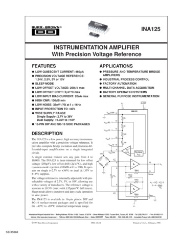
INA125 INA125INA125INSTRUMENTATION AMPLIFIERWith Precision Voltage ReferenceFEATURESAPPLICATIONS LOW QUIESCENT CURRENT: 460µA PRECISION VOLTAGE REFERENCE:1.24V, 2.5V, 5V or 10V SLEEP MODE LOW OFFSET VOLTAGE: 250µV max PRESSURE AND TEMPERATURE BRIDGEAMPLIFIERS LOW OFFSET DRIFT: 2µV/ C max LOW INPUT BIAS CURRENT: 20nA max HIGH CMR: 100dB min BATTERY OPERATED SYSTEMS GENERAL PURPOSE INSTRUMENTATION INDUSTRIAL PROCESS CONTROL FACTORY AUTOMATION MULTI-CHANNEL DATA ACQUISITIONSLEEPV LOW NOISE: 38nV/ Hz at f 1kHz INPUT PROTECTION TO 40V1 WIDE SUPPLY RANGESingle Supply: 2.7V to 36VDual Supply: 1.35V to 18V2INA125VREFCOM 12R13VREFBG 16-PIN DIP AND SO-16 SOIC PACKAGESR14VREF2.5DESCRIPTION2RThe INA125 is a low power, high accuracy instrumentation amplifier with a precision voltage reference. Itprovides complete bridge excitation and precision differential-input amplification on a single integratedcircuit.A single external resistor sets any gain from 4 to10,000. The INA125 is laser-trimmed for low offsetvoltage (250µV), low offset drift (2µV/ C), and highcommon-mode rejection (100dB at G 100). It operates on single ( 2.7V to 36V) or dual ( 1.35V to 18V) supplies.15VREF54RVREF10 16410VThe voltage reference is externally adjustable with pinselectable voltages of 2.5V, 5V, or 10V, allowing usewith a variety of transducers. The reference voltage isaccurate to 0.5% (max) with 35ppm/ C drift (max).Sleep mode allows shutdown and duty cycle operationto save power.The INA125 is available in 16-pin plastic DIP andSO-16 surface-mount packages and is specified forthe –40 C to 85 C industrial temperature range.VREFOutRefAmpBandgapVREF VIN610A1VO930kΩRG11Sense10kΩ10kΩ –) GVO (VIN – VIN87–VING 4 60kΩRGA230kΩIAREF53V–International Airport Industrial Park Mailing Address: PO Box 11400, Tucson, AZ 85734 Street Address: 6730 S. Tucson Blvd., Tucson, AZ 85706 Tel: (520) 746-1111 Twx: 910-952-1111Internet: http://www.burr-brown.com/ FAXLine: (800) 548-6133 (US/Canada Only) Cable: BBRCORP Telex: 066-6491 FAX: (520) 889-1510 Immediate Product Info: (800) 548-6132 1997 Burr-Brown CorporationSBOS060PDS-1361BPrinted in U.S.A., February, 1998
SPECIFICATIONS: VS 15VAt TA 25 C, VS 15V, IA common 0V, VREF common 0V, and RL 10kΩ, unless otherwise noted.INA125P, UPARAMETERCONDITIONSINPUTOffset Voltage, RTIInitialvs Temperaturevs Power SupplyLong-Term StabilityImpedance, DifferentialCommon-ModeSafe Input VoltageInput Voltage RangeCommon-Mode RejectionVS 1.35V to 18V, G 4INA125PA, UATYPMAX 50 0.25 3 0.21011 21011 9 250 2 20MINTYPMAXUNITS 500 5 50µVµV/ CµV/VµV/moΩ pFΩ pFV 40 See TextVCM –10.7V to 10.2VG 4G 10G 100G 500BIAS CURRENTvs TemperatureOffset Currentvs TemperatureVCM 0VNOISE, RTIVoltage Noise, f 10Hzf 100Hzf 1kHzf 0.1Hz to 10HzCurrent Noise, f 10Hzf 1kHzf 0.1Hz to 10HzRS 0ΩGAINGain EquationRange of GainGain ErrorMIN7886100100849411411410 60 0.5 0.572809090 25 2.550 5nApA/ CnApA/ CnV/ HznV/ HznV/ HzµVp-pfA/ HzfA/ HzpAp-p 4 60kΩ/RGVO –14V to 13.3VG 4G 10G 100G 500dBdBdBdB 4038380.81705654 10,000 V/VV/V 0.01 0.03 0.05 0.1 0.075 0.3 0.5 0.1 0.5 1%%%% 1 25 15 100 ppm/ Cppm/ C 0.0004 0.0004 0.001 0.002 0.002 0.002 0.01 0.004 0.004 Gain vs TemperatureG 4G 4(1)VO –14V to 13.3VG 4G 10G 100G 500NonlinearityOUTPUTVoltage: PositiveNegativeLoad Capacitance StabilityShort-Circuit CurrentVOLTAGE REFERENCEAccuracyvs Temperaturevs Power Supply, V vs LoadDropout Voltage, (V ) – VREF(2)Bandgap Voltage ReferenceAccuracyvs Temperature(V )–1.7(V–) 1VREF 2.5V, 5V, 10VIL 0IL 0V (VREF 1.25V) to 36VIL 0 to 5mARef Load 2kΩ1.25IL 0IL 0 (V )–0.9(V–) 0.41000–9/ 12 0.15 18 20311.24 0.5 18 0.5 35 5075 %%%%ofofofofFSFSFSFSVVpFmA 1 100 100 %ppm/ Cppm/Vppm/mAVV%ppm/ CThe information provided herein is believed to be reliable; however, BURR-BROWN assumes no responsibility for inaccuracies or omissions. BURR-BROWN assumesno responsibility for the use of this information, and all use of such information shall be entirely at the user’s own risk. Prices and specifications are subject to changewithout notice. No patent rights or licenses to any of the circuits described herein are implied or granted to any third party. BURR-BROWN does not authorize or warrantany BURR-BROWN product for use in life support devices and/or systems. INA1252
SPECIFICATIONS: VS 15V(CONT)At TA 25 C, VS 15V, IA common 0V, VREF common 0V, and RL 10kΩ, unless otherwise noted.INA125P, UPARAMETER CONDITIONSFREQUENCY RESPONSEBandwidth, –3dBSlew RateSettling Time, 0.01%Overload RecoveryPOWER SUPPLYSpecified Operating VoltageSpecified Voltage RangeQuiescent Current, PositiveNegativeReference Ground Current(3)Sleep Current (VSLEEP 100mV)MING 4G 10G 100G 500G 4, 10V StepG 4, 10V StepG 10, 10V StepG 100, 10V StepG 500, 10V Step50% OverdriveINA125PA, UAMAXMINIO IREF 0mAIO IREF 0mA 15460–280180 1RL 10kΩ, Ref Load 2kΩ 2.70 25V 0.1–40–55–55MAX VVµAµAµs C C C C/W C/W 80100VVµAµAµAµA 85 125 125UNITSkHzkHzkHzkHzV/µsµsµsµsµsµs 18525–325150150TEMPERATURE RANGESpecification RangeOperation RangeStorage RangeThermal Resistance, θJA16-Pin DIPSO-16 Surface-MountTYP 150454.50.90.2608337517005 1.35SLEEP MODE PIN(4)VIH (Logic high input voltage)VIL (Logic low input voltage)IIH (Logic high input current)IIL (Logic low input current)Wake-up Time(5)TYP Specification same as INA125P, U.NOTES: (1) Temperature coefficient of the "Internal Resistor" in the gain equation. Does not include TCR of gain-setting resistor, RG. (2) Dropout voltage is thepositive supply voltage minus the reference voltage that produces a 1% decrease in reference voltage. (3) VREFCOM pin. (4) Voltage measured with respect toReference Common. Logic low input selects Sleep mode. (5) IA and Reference, see Typical Performance Curves.SPECIFICATIONS: VS 5VAt TA 25 C, VS 5V, IA common at VS /2, VREF common VS /2, VCM VS/2, and RL 10kΩ to VS/2, unless otherwise noted.INA125P, UPARAMETERINPUTOffset Voltage, RTIInitialvs Temperaturevs Power SupplyInput Voltage RangeCommon-Mode RejectionGAINGain ErrorCONDITIONSVS 2.7V to 36VVCM 1.1V to 3.6VG 4G 10G 100G 5007886100100VO 0.3V to 3.8VG 4OUTPUTVoltage, PositiveNegativePOWER SUPPLYSpecified Operating VoltageOperating Voltage RangeQuiescent CurrentSleep Current (VSLEEP 100mV)MININA125PA, UATYPMAX 75 0.253See Text 500MIN20849411411472809090 0.01(V )–1.2(V–) 0.3 (V )–0.8(V–) 0.15IO IREF 0mARL 10kΩ, Ref Load 2kΩ460 1MAXUNITS 750µVµV/ CµV/V50 dBdBdBdB % VV 5 2.7TYP 36525 25 VVµAµA Specification same as INA125P, U. 3INA125
ABSOLUTE MAXIMUM RATINGS(1)PIN CONFIGURATIONTop View16-Pin DIP, SO-16V 116 VREF10SLEEP215 VREF5V–314 VREF2.5VREFOUT413 VREFBGIAREF512 VREFCOM VIN611 Sense–VIN710 VORG89Power Supply Voltage, V to V– . 36VInput Signal Voltage . 40VOutput Short Circuit . ContinuousOperating Temperature . –55 C to 125 CStorage Temperature . –55 C to 125 CLead Temperature (soldering, 10s) . 300 CNOTE: Stresses above these ratings may cause permanent damage.PACKAGE INFORMATIONRGPRODUCTPACKAGEPACKAGE DRAWINGNUMBER(1)INA125PAINA125P16-Pin Plastic DIP16-Pin Plastic DIP180180INA125UAINA125USO-16 Surface-MountSO-16 Surface-Mount265265NOTES: (1) For detailed drawing and dimension table, please see end of datasheet, or Appendix C of Burr-Brown IC Data Book.ELECTROSTATICDISCHARGE SENSITIVITYThis integrated circuit can be damaged by ESD. Burr-Brownrecommends that all integrated circuits be handled with appropriate precautions. Failure to observe proper handling andinstallation procedures can cause damage.ESD damage can range from subtle performance degradationto complete device failure. Precision integrated circuits maybe more susceptible to damage because very small parametricchanges could cause the device not to meet its publishedspecifications. INA1254
TYPICAL PERFORMANCE CURVESAt TA 25 C and VS 15V, unless otherwise noted.COMMON-MODE REJECTION vs FREQUENCYGAIN vs FREQUENCY60120G 500Common-Mode Rejection (dB)G 100, 50050G 100Gain (dB)4030G 1020G 41080G 1060G 500G 440G 10020001101001k10k100k1M1101001k10k100kFrequency (Hz)Frequency (Hz)POSITIVE POWER SUPPLY REJECTIONvs FREQUENCYNEGATIVE POWER SUPPLY REJECTIONvs FREQUENCY1401M120120Power Supply Rejection (dB)Power Supply Rejection (dB)100G 500100G 10080G 460G 1040100G 10080G 5006040G 1020G 4200101001k10k1M11001k10k100kINPUT COMMON-MODE VOLTAGEvs OUTPUT VOLTAGE, VS 15VINPUT COMMON-MODE VOLTAGEvs OUTPUT VOLTAGE, VS 5V105VD/20– VD/2VOIAREF– VCM–5 15V –15V–10tput swing—seeLimited by A2 outextIAREF 0V4–50510152textVS 5V10–1VS 5V–2–3–4tput swing—seeLimited by A2 ou–5Output Voltage (V)tput swing—seeLimited by A2 ou3–5–101M5texttput swing—seeLimited by A2 ou–15–1510Frequency (Hz)15Input Common-Mode Voltage (V)100kFrequency (Hz)Input Common-Mode Voltage (V)1–4–3–2–1012text345Output Voltage (V) 5INA125
TYPICAL PERFORMANCE CURVES(CONT)At TA 25 C and VS 15V, unless otherwise noted.SETTLING TIME vs GAIN10k1kCurrent Noise100100Voltage Noise101011101001kSettling Time (µs)1kInput Bias Current Noise (fA/ Hz)Input-Referred Voltage Noise (nV/ Hz)INPUT-REFERRED VOLTAGE AND CURRENT NOISEvs FREQUENCY11kINPUT-REFERRED OFFSET VOLTAGEvs SLEEP TURN-ON TIMEQUIESCENT CURRENT AND SLEEP CURRENTvs TEMPERATURE60Quiescent and Sleep Current (µA)Offset Voltage Change (µV)100Gain (V/V)80G 0450400350 IQ300250200150100500–50250 ISLEEP–IQVSLEEP 100mV ISLEEPVSLEEP 0V–ISLEEP–75–50–250255075Time From Turn-On (µs)Temperature ( C)SLEW RATE vs TEMPERATUREINPUT BIAS AND OFFSET CURRENTvs TEMPERATURE0.30100125100125Input Bias and Offset Current (nA)160.25Slew Rate (V/µs)10Frequency mperature ( C)–2502550Temperature ( C) INA125–50675
TYPICAL PERFORMANCE CURVES(CONT)At TA 25 C and VS 15V, unless otherwise noted.LARGE-SIGNAL RESPONSESMALL-SIGNAL RESPONSEG 45V/div200mV/divG 4G 100G 100100µs/div100µs/divINPUT BIAS CURRENTvs INPUT OVERLOAD VOLTAGEINPUT-REFERRED NOISE, 0.1Hz to 10Hz200200nV/divInput Bias Current (µA)160All /div040Overload Voltage (V)OUTPUT VOLTAGE SWINGvs OUTPUT CURRENTDELTA VOS vs REFERENCE CURRENT25 75 C20 25 C 125 C(V )–3(V )–4(V )–5Delta VOS, RTI (µV)Output Voltage (V)V (V )–1(V )–2–55 C(V–) 5(V–) 4 75 C(V–) 3(V–) 2(V–) 1–55 CSinking15105Sourcing0 125 C 25 CV––50 2 4 6 8–8 10Output Current (mA)–6–4–202468Reference Current (mA) 7INA125
TYPICAL PERFORMANCE CURVES(CONT)At TA 25 C and VS 15V, unless otherwise noted.INPUT-REFERRED OFFSET VOLTAGEPRODUCTION DISTRIBUTION, VS 15VINPUT-REFERRED OFFSET VOLTAGEPRODUCTION DISTRIBUTION, VS 5V3035Typical productiondistribution ofpackaged 253003754505256006757500Input-Referred Offset Voltage (µV)Input-Referred Offset Voltage (µV)VOLTAGE REFERENCE DRIFTPRODUCTION DISTRIBUTIONINPUT-REFERRED OFFSET VOLTAGE DRIFTPRODUCTION DISTRIBUTION10040300.2%1000.05%10 4.00 3.75 3.50 3.25 3.00 2.75 2.50 2.25 2.00 1.75 1.50 1.250 1.000 0.7510 0.5010 0.250.3%2090205080306050407040VS 15V or 5V306080207050Typical productiondistribution of packaged units.90Percent of Amplifiers (%)8070Typical productiondistribution of packaged units.6090Percent of Amplifiers (%)0.1%50.1%0.02%Typical productiondistribution ofpackaged units.30Percent of Amplifiers (%)Percent of Amplifiers (%)25Voltage Reference Drift (ppm/ C)Input-Referred Offset Voltage Drift (µV/ C)REFERENCE VOLTAGE DEVIATIONvs TEMPERATUREREFERENCE TURN-ON SETTLING TIME50Reference Voltage Deviation (ppm)1512Reference Error (%)9640–3VREF 10V–6VREF 5V–9–12VREF re ( C)Time From Power Supply Turn-On (µs) INA125–50–200–75–150VREF VBG, 2.5V, 5V, or 10V0875100125
TYPICAL PERFORMANCE CURVES(CONT)At TA 25 C and V S 15V, unless otherwise noted.0.1Hz to 10Hz REFERENCE NOISEVREF 2.5V, CL 100pF1mA/divREFERENCE TRANSIENT RESPONSEVREF 2.5V, CL 100pF v10µs/divNEGATIVE REFERENCE AC LINE REJECTIONvs FREQUENCYPOSITIVE REFERENCE AC LINE REJECTIONvs FREQUENCY120VREF 2.5V100VREF 5VNegative AC Line Rejection (dB)Positive AC Line Rejection (dB)12080VREF 10VC 0.01µF60C 0.1µF40Capacitor connected betweenVREFOUT and VREFCOM.20VREF 2.5V100VREF 5V80VREF ency (Hz)Frequency (Hz) 9INA125
APPLICATION INFORMATIONFor example, in Figure 1 VREFOUT is connected to VREF10thus supplying 10V to the bridge. It is recommended thatVREFOUT be connected to one of the reference voltage pinseven when the reference is not being utilized to avoidsaturating the reference amplifier. Driving the SLEEP pinLOW puts the INA125 in a shutdown mode.Figure 1 shows the basic connections required for operationof the INA125. Applications with noisy or high impedancepower supplies may require decoupling capacitors close tothe device pins as shown.The output is referred to the instrumentation amplifier reference (IAREF) terminal which is normally grounded. Thismust be a low impedance connection to assure good common-mode rejection. A resistance of 12Ω in series with theIAREF pin will cause a typical device to degrade to approximately 80dB CMR (G 4).SETTING THE GAINGain of the INA125 is set by connecting a single externalresistor, RG, between pins 8 and 9:G 4 Connecting VREFOUT (pin 4) to one of the four availablereference voltage pins (VREFBG, VREF2.5, VREF5, or VREF10)provides an accurate voltage source for bridge applications.60kΩRG(1)Commonly used gains and RG resistor values are shown inFigure 1.V SLEEP(1)0.1µF21DESIRED GAIN(V/V)RG(Ω)NEAREST 1%RG VALUE 6.04INA125VREFCOM 12R(2)13VREFBGR14VREF2.52R15VREF54RVREF10 16NC: No Connection.410VVREFOutRefAmpBandgapVREF – V –) GVO (VINING 4 60kΩRG VIN610A1930kΩSense10kΩRG11 10kΩLoad87–VINA230kΩIAREF5NOTE: (1) SLEEP pin should be connectedto V if shutdown function is not being used.(2) Nominal value of R is 21kΩ, 25%.30.1µFV–FIGURE 1. Basic Connections. INA12510VO–
INPUT COMMON-MODE RANGEThe 60kΩ term in equation 1 comes from the internal metalfilm resistors which are laser trimmed to accurate absolutevalues. The accuracy and temperature coefficient of theseresistors are included in the gain accuracy and drift specifications of the INA125.The input common-mode range of the INA125 is shown inthe typical performance curves. The common-mode range islimited on the negative side by the output voltage swing ofA2, an internal circuit node that cannot be measured on anexternal pin. The output voltage of A2 can be expressed as:V 1.3V – – (V – V – ) (10kΩ/R )The stability and temperature drift of the external gainsetting resistor, RG, also affects gain. RG’s contribution togain accuracy and drift can be directly inferred from the gainequation (1). Low resistor values required for high gain canmake wiring resistance important. Sockets add to the wiringresistance, which will contribute additional gain error (possibly an unstable gain error) in gains of approximately 100or greater.02V The on-board precision voltage reference provides an accurate voltage source for bridge and other transducer applications or ratiometric conversion with analog-to-digital converters. A reference output of 2.5V, 5V or 10V is availableby connecting VREFOUT (pin 4) to one of the VREF pins(VREF2.5, VREF5, or VREF10). Reference voltages are lasertrimmed for low inital error and low temperature drift.Connecting VREFOUT to VREFBG (pin 13) produces thebandgap reference voltage (1.24V 0.5%) at the referenceoutput.100µA1/2 REF200IAREFINOPA23710kΩGPRECISION VOLTAGE REFERENCEV VOINA125INThe internal op amp A2 is identical to A1. Its output swingis limited to approximately 0.8V from the positive supplyand 0.25V from the negative supply. When the input common-mode range is exceeded (A2’s output is saturated), A1can still be in linear operation, responding to changes in thenon-inverting input voltage. The output voltage, however,will be invalid.The INA125 is laser trimmed for low offset voltage andoffset voltage drift. Most applications require no externaloffset adjustment. Figure 2 shows an optional circuit fortrimming the output offset voltage. The voltage applied tothe IAREF terminal is added to the output signal. The op ampbuffer is used to provide low impedance at the IAREFterminal to preserve good common-mode rejection.RGIN(voltages referred to IAREF terminal, pin 5)OFFSET TRIMMING–VININPositive supply voltage must be 1.25V above the desiredreference voltage. For example, with V 2.7V, only the1.24V reference (VREFBG) can be used. If using dual supplies VREFCOM can be connected to V–, increasing the100Ω 10mVAdjustment Range100Ω100µA1/2 REF200Microphone,Hydrophoneetc.INA125V–FIGURE 2. Optional Trimming of Output Offset Voltage.47kΩ47kΩINPUT BIAS CURRENT RETURNThe input impedance of the INA125 is extremely high—approximately 1011Ω. However, a path must be provided forthe input bias current of both inputs. This input bias currentflows out of the device and is approximately 10nA. Highinput impedance means that this input bias current changesvery little with varying input voltage.ThermocoupleINA12510kΩInput circuitry must provide a path for this input bias currentfor proper operation. Figure 3 shows various provisions foran input bias current path. Without a bias current path, theinputs will float to a potential which exceeds the commonmode range, and the input amplifiers will saturate.INA125If the differential source resistance is low, the bias currentreturn path can be connected to one input (see the thermocouple example in Figure 3). With higher source impedance,using two equal resistors provides a balanced input withpossible advantages of lower input offset voltage due to biascurrent and better high frequency common-mode rejection.Center-tap providesbias current return.FIGURE 3. Providing an Input Common-Mode Current Path. 11INA125
A transition region exists when VSLEEP is between 400mVand 2.7V (with respect to VREFCOM) where the output isunpredictable. Operation in this region is not recommended.The INA125 achieves high accuracy quickly following wakeup (VSLEEP 2.7V). See the typical performance curve“Input-Referred Offset Voltage vs Sleep Turn-on Time.” Ifshutdown is not being used, connect the SLEEP pin to V .amount of supply voltage headroom available to the reference. Approximately 180µA flows out of the VREFCOMterminal, therefore, it is recommended that it be connectedthrough a low impedance path to sensor common to avoidpossible ground loop problems.Reference noise is proportional to the reference voltageselected. With VREF 2.5V, 0.1Hz to 10Hz peak-to-peaknoise is approximately 9µVp-p. Noise increases to 36µVp-pfor the 10V reference. Output drive capability of the voltagereference is improved by connecting a transistor as shown inFigure 4. The external transistor also serves to remove powerfrom the INA125.LOW VOLTAGE OPERATIONThe INA125 can be operated on power supplies as low as 1.35V. Performance remains excellent with power supplies ranging from 1.35V to 18V. Most parameters varyonly slightly throughout this supply voltage range—seetypical performance curves. Operation at very low supplyvoltage requires careful attention to ensure that the common-mode voltage remains within its linear range. See“Input Common-Mode Voltage Range.” As previously mentioned, when using the on-board reference with low supplyvoltages, it may be necessary to connect VREFCOM to V– toensure VS – VREF 1.25V.Internal resistors that set the voltage reference output areratio-trimmed for accurate output voltages ( 0.5% max). Theabsolute resistance values, however, may vary 25%. Adjustment of the reference output voltage with an external resistoris not recommended because the required resistor value isuncertain.VREFCOMINA125SINGLE SUPPLY OPERATION12The INA125 can be used on single power supplies of 2.7Vto 36V. Figure 5 shows a basic single supply circuit. TheIAREF, VREFCOM, and V– terminals are connected to ground.Zero differential input voltage will demand an output voltage of 0V (ground). When the load is referred to ground asshown, actual output voltage swing is limited to approximately 150mV above ground. The typical performance curve“Output Voltage Swing vs Output Current” shows how theoutput swing varies with output current.13VREFBGVREF2.5VREF5VREF101415With single supply operation, careful attention should bepaid to input common-mode range, output voltage swing ofboth op amps, and the voltage applied to the IAREF terminal.VIN and VIN– must both be 1V above ground for linearoperation. You cannot, for instance, connect the invertinginput to ground and measure a voltage connected to the noninverting input.16V 4TIP29CVREFOutRefAmpBandgapVREF10Vto load(transducer) 3V 3VFIGURE 4. Reference Current Boost.1.5V – VSHUTDOWN1000ΩThe INA125 has a shutdown option. When the SLEEP pinis LOW (100mV or less), the supply current drops toapproximately 1µA and output impedance becomes approximately 80kΩ. Best performance is achieved with CMOSlogic. To maintain low sleep current at high temperatures,VSLEEP should be as close to 0V as possible. This should notbe a problem if using CMOS logic unless the CMOS gate isdriving other currents. Refer to the typical performancecurve, “Sleep Current vs Temperature.”1.5V V12VOINA1251253FIGURE 5. Single Supply Bridge Amplifier. INA125RGRL
INPUT PROTECTIONThe inputs of the INA125 are individually protected forvoltage up to 40V. For example, a condition of –40V onone input and 40V on the other input will not causedamage. Internal circuitry on each input provides low seriesimpedance under normal signal conditions. To provideequivalent protection, series input resistors would contributeexcessive noise. If the input is overloaded, the protectioncircuitry limits the input current to a safe value of approximately 120µA to 190µA. The typical performance curve“Input Bias Current vs Input Overload Voltage” shows thisinput current limit behavior. The inputs are protected even ifthe power supplies are disconnected or turned off.SLEEP 5V21INA125VREFCOM EF2.5V VIN610A1930kΩSense10kΩRG11 10kΩLoad87–VIN –VO 2.5V [(VIN– VIN) (4 OTE: (1) “Psuedoground” is at 2.5V above actual ground.This provides a precision reference voltage for succeedingsingle-supply op amp stages.FIGURE 6. Psuedoground Bridge Measurement, 5V Single Supply. 13INA125
PACKAGE OPTION ADDENDUMwww.ti.com7-Oct-2021PACKAGING INFORMATIONOrderable DeviceStatus(1)Package Type Package Pins PackageDrawingQtyEco Plan(2)Lead finish/Ball materialMSL Peak TempOp Temp ( C)Device Marking(3)(4/5)(6)INA125PACTIVEPDIPN1625RoHS & GreenCall TIN / A for Pkg Type-40 to 85INA125PINA125PAACTIVEPDIPN1625RoHS & GreenCall TIN / A for Pkg TypeINA125PAINA125PAG4ACTIVEPDIPN1625RoHS & GreenCall TIN / A for Pkg TypeINA125PAINA125UACTIVESOICD1640RoHS & GreenCall TILevel-3-260C-168 HRINA125UAINA125U/2K5ACTIVESOICD162500RoHS & GreenCall TILevel-3-260C-168 HRINA125UAINA125UAACTIVESOICD1640RoHS & GreenCall TILevel-3-260C-168 HRINA125UAINA125UA/2K5ACTIVESOICD162500RoHS & GreenCall TILevel-3-260C-168 HRINA125UA(1)The marketing status values are defined as follows:ACTIVE: Product device recommended for new designs.LIFEBUY: TI has announced that the device will be discontinued, and a lifetime-buy period is in effect.NRND: Not recommended for new designs. Device is in production to support existing customers, but TI does not recommend using this part in a new design.PREVIEW: Device has been announced but is not in production. Samples may or may not be available.OBSOLETE: TI has discontinued the production of the device.(2)RoHS: TI defines "RoHS" to mean semiconductor products that are compliant with the current EU RoHS requirements for all 10 RoHS substances, including the requirement that RoHS substancedo not exceed 0.1% by weight in homogeneous materials. Where designed to be soldered at high temperatures, "RoHS" products are suitable for use in specified lead-free processes. TI mayreference these types of products as "Pb-Free".RoHS Exempt: TI defines "RoHS Exempt" to mean products that contain lead but are compliant with EU RoHS pursuant to a specific EU RoHS exemption.Green: TI defines "Green" to mean the content of Chlorine (Cl) and Bromine (Br) based flame retardants meet JS709B low halogen requirements of 1000ppm threshold. Antimony trioxide basedflame retardants must also meet the 1000ppm threshold requirement.(3)MSL, Peak Temp. - The Moisture Sensitivity Level rating according to the JEDEC industry standard classifications, and peak solder temperature.(4)There may be additional marking, which relates to the logo, the lot trace code information, or the environmental category on the device.(5)Multiple Device Markings will be inside parentheses. Only one Device Marking contained in parentheses and separated by a " " will appear on a device. If a line is indented then it is a continuationof the previous line and the two combined represent the entire Device Marking for that device.Addendum-Page 1Samples
PACKAGE OPTION ADDENDUMwww.ti.com7-Oct-2021(6)Lead finish/Ball material - Orderable Devices may have multiple material finish options. Finish options are separated by a vertical ruled line. Lead finish/Ball material values may wrap to twolines if the finish value exceeds the maximum column width.Important Information and Disclaimer:The information provided on this page represents TI's knowledge and belief as of the date that it is provided. TI bases its knowledge and belief on informationprovided by third parties, and makes no representation or warranty as to the accuracy of such information. Efforts are underway to better integrate information from third parties. TI has taken andcontinues to take reasonable steps to provide representative and accurate information but may not have conducted destructive testing or chemical analysis on incoming materials and chemicals.TI and TI suppliers consider certain information to be proprietary, and thus CAS numbers and other limited information may not be available for release.In no event shall TI's liability arising out of such information exceed the total purchase price of the TI part(s) at issue in this document sold by TI to Customer on an annual basis.Addendum-Page 2
PACKAGE MATERIALS INFORMATIONwww.ti.com5-Jan-2022TAPE AND REEL INFORMATION*All dimensions are nominalDevicePackage Package PinsType DrawingSPQReelReelA0Diameter Width (mm)(mm) W1 (mm)B0(mm)K0(mm)P1(mm)WPin1(mm) 8.016.0Q1Pack Materials-Page 1
PACKAGE MATERIALS INFORMATIONwww.ti.com5-Jan-2022*All dimensions are nominalDevicePackage TypePackage DrawingPinsSPQLength (mm)Width (mm)Height K5SOICD162500853.0449.035.0Pack Materials-Page 2
PACKAGE MATERIALS INFORMATIONwww.ti.com5-Jan-2022TUBE*All dimensions are nominalDevicePackage NamePackage TypePinsSPQL (mm)W (mm)T (µm)B 1640506.6839404.32Pack Materials-Page 3
IMPORTANT NOTICE AND DISCLAIMERTI PROVIDES TECHNICAL AND RELIABILITY DATA (INCLUDING DATA SHEETS), DESIGN RESOURCES (INCLUDING REFERENCEDESIGNS), APPLICATION OR OTHER DESIGN ADVICE, WEB TOOLS, SAFETY INFORMATION, AND OTHER RESOURCES “AS IS”AND WITH ALL FAULTS, AND DISCLAIMS ALL WARRANTIES, EXPRESS AND IMPLIED, INCLUDING WITHOUT LIMITATION ANYIMPLIED WARRANTIES OF MERCHANTABILITY, FITNESS FOR A PARTICULAR PURPOSE OR NON-INFRINGEMENT OF THIRDPARTY INTELLECTUAL PROPERTY RIGHTS.These resources are intended for skilled developers designing with TI products. You are solely responsible for (1) selecting the appropriateTI products for your application, (2) designing, validating and testing your application, and (3) ensuring your application meets applicablestandards, and any other safety, security, regulatory or other requirements.These resources are subject to change without notice. TI grants you permission to use these resources only for development of anapplication that uses the TI products described in the resource. Other reproduction and display of these resources is prohibited. No licenseis granted to any other TI intellectual property right or to any third party intellectual property right. TI disclaims responsibility for, and youwill fully indemnify TI and its representatives against, any claims, damages, costs, losses, and liabilities arising out of your use of theseresources.TI’s products are provided subject to TI’s Terms of Sale or other applicable terms available either on ti.com or provided in conjunction withsuch TI products. TI’s provision of these resources does not expand or otherwise alter TI’s applicable warranties or warranty disclaimers forTI products.TI objects to and rejects any additional or different terms you may have proposed. IMPORTANT NOTICEM
INDUSTRIAL PROCESS CONTROL FACTORY AUTOMATION MULTI-CHANNEL DATA ACQUISITION BATTERY OPERATED SYSTEMS GENERAL PURPOSE INSTRUMENTATION DESCRIPTION The INA125 is a low power, high accuracy instrumen-tation amplifier with a precision voltage reference.